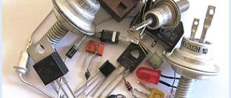
Semiconductor materials.
Also on topic:
ELECTRONICS INDUSTRY
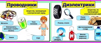
A semiconductor is a material that conducts electricity better than a dielectric such as rubber, but not as well as a good conductor such as copper. Unlike metals, the electrical conductivity of semiconductors increases with increasing temperature. The best semiconductor materials include silicon (Si) and germanium (Ge); others include compounds of gallium (Ga), arsenic (As), phosphorus (P) and indium (In). Silicon has many uses in transistors, rectifiers and integrated circuits. Gallium arsenide (GaAs) is commonly used in microwave and optoelectronic devices, as well as integrated circuits. see also
PERIODIC SYSTEM OF ELEMENTS; INTEGRATED CIRCUIT; SOLID STATE PHYSICS; TRANSISTOR.
A semiconductor is essentially a dielectric until a small and carefully measured amount of some suitable material is introduced into it. For example, a material such as phosphorus makes silicon conductive by adding excess electrons to it (i.e., acting as a “donor”). Silicon doped in this way becomes silicon n
-type.
Doping with a material such as boron transforms silicon into a p
-type material: boron (the acceptor) takes away some of the electrons from the silicon, creating “holes” in it, which can be filled with electrons from nearby atoms and thereby increase the conductivity of the doped material. (The flow of electrons in one direction and holes in the opposite direction forms a current.) The electrons and holes that thus provide conductivity are called charge carriers.
pn-Transitions.
Solid-state electronic devices are usually a multilayer structure (sandwich), one part of which is made of semiconductor p
-type, and the other is from an
n
-type semiconductor.
The boundary region between p
-type and
n
-type materials is called
p-n
junction.
The transition is formed by positively charged atoms of the donor impurity on the n
side and negatively charged atoms of the acceptor impurity on
the p
side.
The electric field created by these ions prevents the diffusion of electrons into the p
region and holes into
the n
region (Fig. 1).
If p
p-n
region is connected to the positive terminal of a voltage source (for example, a battery), and the
n
region is connected to the negative terminal, then electrons and holes can diffuse through the junction.
As a result, a significant current will flow from the p
-region in the direction of
the n
-region.
In this case, the transition is said to be forward biased. In reverse bias, when the connections described above are of opposite polarity, only a very small amount of reverse current will flow from the n
-type region to the
p
-type region.
Modern semiconductor manufacturing technologies
In recent years, a number of technologies have approached the stage of being able to be used in commercial production, making it possible to significantly increase the speed of transistors, or to significantly reduce the size of the chip without switching to a finer technological process. Some of these technologies have already begun to be used in recent months, and their names are being mentioned more often in computer-related news. This article is an attempt to give a brief overview of such technologies, trying to look into the very near possible future of the chips found in our computers.
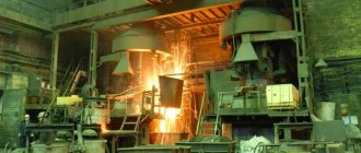
The first integrated circuit, where connections between transistors are made directly on the substrate, was made more than 40 years ago. During this time, their production technology has undergone a number of large and small improvements, moving from Jack Kilby's first circuit to today's central processors, consisting of tens of millions of transistors, although for server processors we can already talk about hundreds of millions.
Here we will talk about some of the latest technologies in this area, such as copper conductors in chips, SiGe, SOI, perovskites. But first, it is necessary to briefly touch on the traditional process of producing chips from silicon wafers. There is no need to describe the process of turning sand into wafers, since all these technologies have nothing to do with such basic steps, so let's start with the fact that we already have a silicon wafer, the diameter of which in most of today's factories using modern technologies is 20 cm. The next step in its transformation into chips is the process of oxidizing its surface, covering it with a film of oxides - SiO2, which is an excellent insulator and protects the surface of the wafer during lithography.
Next, another protective layer is applied to the wafer, this time a photosensitive one, and one of the key operations occurs - removing unnecessary areas of it and the oxide film from the surface of the wafer in certain places, until pure silicon is exposed, using photolithography.
At the first stage, a plate with a film of a photosensitive layer applied to its surface is placed in an exposure unit, which essentially works like a photographic enlarger. A precision mask is used here as a negative - a square plate of quartz glass coated with a chromium film where required. The chromed and exposed areas form a 1:5 scale image of one layer of one chip. Based on special signs pre-formed on the surface of the wafer, the installation automatically aligns the wafer, adjusts the focus and illuminates the photosensitive layer through a mask and a lens system with reduction so that an image of the crystal is obtained on the wafer on a scale of 1:1. The wafer is then shifted, the next die is exposed, and so on until all the chips on the wafer have been processed. The mask itself is also formed by a photochemical method, only the illumination of the photosensitive layer during the formation of the mask occurs according to a program with an electron beam in much the same way as in a television kinescope.
As a result of exposure, the chemical composition of those areas of the photosensitive layer that fall under the transparent areas of the photomask changes. This makes it possible to remove them using appropriate chemicals or other methods such as plasma or x-rays.
After which a similar procedure (using other substances, of course) is applied to the layer of oxides on the surface of the plate. And again, again, using new chemicals, the photosensitive layer is removed:
Then the next mask is applied, with a different template, then another, another, and another... It is this stage of chip production that is critical in terms of errors: any speck of dust or microscopic shift to the side when applying the next mask, and the chip can already go to the landfill. Once the chip structure is formed, it is time to change the atomic structure of the silicon in the desired areas by adding various impurities. This is required in order to obtain regions of silicon with different electrical properties - p-type and n-type, that is, exactly what is required to create a transistor. Boron, gallium, and aluminum are used to form p-regions, and antimony, arsenic, and phosphorus are used to create n-regions.
The surface of the wafer is thoroughly cleaned so that no excess substances get into the silicon along with impurities, after which it enters a chamber for high-temperature treatment and a small amount of the required impurities is applied to it, in one or another state of aggregation, with or without the use of ionization. After which, at a temperature of the order of 700 to 1400 degrees, the process of diffusion occurs, the penetration of the required elements into the silicon in its areas exposed during the lithography process. As a result, areas with the desired properties are obtained on the surface of the plate. And at the end of this stage, the same protective film of silicon oxide, about one micron thick, is applied to their surface.
All. All that remains is to lay metal connections along the surface of the chip (today aluminum is usually used for this role, and the connections today are usually arranged in 6 layers), and the job is done. In general terms, this is how the result is, for example, a classic MOS transistor: when there is a voltage on the gate, electrons begin to move between the modified regions of the silicon.
Now, having briefly gone over the classical process of creating today's chips, we can more confidently move on to a review of technologies that involve making certain adjustments to this picture.
Copper connections
IBM CMOS 7S process, the first copper technology to be used in commercial chip production
The first of them, which has already begun to be widely introduced into commercial production, is the replacement of aluminum with copper at the last stage. Copper is a better conductor than aluminum (resistivity 0.0175 versus 0.028 ohm*mm2/m), which, in full accordance with the laws of physics, makes it possible to reduce the cross-section of intercomponent connections. Quite timely, given the constant movement of the industry towards reducing the size of transistors and increasing the density of their placement on the chip, when the use of aluminum begins to become impossible. The industry began to face this problem already in the first half of the 90s. In addition, what is the point of accelerating the transistors themselves if the connections between them will eat up the entire speed increase?
The problem when switching to copper was that aluminum forms contact with silicon much better. However, after decades of research, scientists managed to find a principle for creating an ultra-thin separating region between the silicon substrate and copper conductors, preventing the diffusion of these two materials.
According to IBM, using copper instead of aluminum in the process can reduce costs by about 20-30 percent by reducing the area of the chip. Their CMOS 7S technology, using copper connections, allows the creation of chips containing up to 150-200 million transistors. And finally, a simple increase in chip performance (up to 40 percent) due to lower conductor resistance.
IBM began offering this technology to customers in early 98, at the end of that year its customers were offered to use copper in the production of their TSMC and UMC chips, AMD begins producing copper Athlons in early 2000, Intel switches to copper in 2002, simultaneously with the transition to 0.13 micron technical process.
SiGe
Connections are connections, but already at a chip speed of several GHz, the silicon substrate itself can no longer cope with the load. And while silicon chips are still sufficient for traditional applications, in the field of wireless communications there has long been a shortage of cheap, high-speed chips. Silicon is cheap but slow, gallium arsenide is fast but expensive. The solution here was to use a compound of two fundamentals of the semiconductor industry - silicon with germanium, SiGe - as a material for substrates. Practical results on this technology began to appear in the late 80s. The first bipolar transistor made using SiGe (using germanium as the base material) was demonstrated in 1987. In 1992, it became possible to use standard CMOS technology with a resolution of 0.25 microns in the production of chips with SiGe transistors.
The result of the application is an increase in the speed of chips by 2-4 times compared to what can be achieved using silicon, and their power consumption is reduced by the same amount. At the same time, the same decisive factor comes into play - cost: SiGe chips can be produced on the same lines that are used to produce chips based on conventional silicon wafers, thus eliminating the need for expensive retooling of production equipment. According to IBM, the potential speed of a transistor (not a chip!) with their technology today is 45-50 GHz (which is far from a record), work is underway to increase this figure to 120 GHz. However, you should not expect the arrival of SiGe in computers in the coming years - at the speeds that PC chips will require in the near future, silicon doped with technologies such as copper connections or SOI will be sufficient.
Silicon-on-insulator (SOI)
Another technology that allows you to fairly painlessly increase the speed of chips, without requiring manufacturers to abandon all their current developments. Like copper interconnect technology, SOI allows chip makers to kill two birds with one stone—increasing speed by up to 25 percent while reducing power consumption. What is this technology? Let's remember the beginning of processing a silicon wafer - it is covered with a thin film of silicon oxide. And in SOI one more element is added to this sandwich - a thin layer of silicon is again applied on top:
So it turns out - silicon on an insulator. Why was this needed? To reduce capacity. Ideally, the MOSFET should turn off as soon as the gate power disappears (or vice versa, in the case of CMOS). But our world is far from ideal, and this is also true in this particular case. The response time of the transistor is directly affected by the capacitance of the region between the modified sections of silicon, through which the current flows when the transistor is turned on. It does not start and stop walking instantly, but only after, respectively, charging and discharging this intermediate zone. It is clear that the shorter this time, the faster the transistor operates; we can say that the less its inertia. This is why SOI was invented - if there is a thin plate of an insulating substance (silicon oxide, glass, etc.) between the modified areas and the bulk of the silicon, this issue is removed and the transistor begins to work noticeably faster.
The main difficulty in this case, as in the case of copper compounds, lies in the different physical properties of the substance. The silicon used in the substrate is a crystal, the oxide film is not, and it is very difficult to attach another layer of crystalline silicon to its surface, or to the surface of another insulator. It was precisely the problem of creating the perfect layer that took a lot of time. IBM has recently demonstrated PowerPC processors and SRAM chips built using this technology, signaling that SOI has reached the stage of commercialization. Most recently, IBM announced that it has achieved the ability to combine SOI and copper on a single chip, taking advantage of the benefits of both technologies. However, so far no one except her has publicly announced their intention to use this technology in the production of chips, although something similar is being discussed.
Perovskites
The search for a replacement for the role of an insulating film on the surface of the substrate has been going on for a long time, given that, like aluminum, silicon dioxide has recently begun to fail - with a constant increase in the density of transistors on a chip, it is necessary to reduce the thickness of its insulating layer, and this has a limit set by its electrical properties , which is already pretty close. However, despite all attempts, SiO2 is still in its place. At one time, IBM intended to use polyamide in this role, now it’s Motorola’s turn to come up with its own option - perovskites.
This class of minerals is quite rare in nature - Tanzania, Brazil and Canada, but can be grown artificially. Perovskite crystals are distinguished by very high dielectric properties: the strontium titanate used by Motorola exceeds silicon dioxide in this parameter by more than an order of magnitude. And this makes it possible to reduce the thickness of transistors by three to four times compared to using the traditional approach. Which, in turn, makes it possible to significantly reduce the leakage current, making it possible to significantly increase the density of transistors on the chip, while at the same time greatly reducing its power consumption.
While this technology is still in its early stages of development, Motorola has already demonstrated the ability to deposit a film of perovskites on the surface of a standard 20 cm silicon wafer, as well as a working CMOS transistor based on this technology.
Thanks to Igor Chudakov for his help in creating this article
PN Junction Diodes.
Diodes are devices that conduct electrical current in only one direction. Therefore pn
-transitions are ideal for use in diode rectifiers that convert alternating current to direct current.
When the reverse bias voltage on a pn
-transition increases to a critical value, called the breakdown voltage, the electric field in the transition region creates electrons and holes as a result of collisions of high-energy charge carriers with semiconductor atoms. During this process, called ionization, an “avalanche” of new carriers is formed, as a result of which the reverse current at the breakdown voltage increases significantly.
Diode rectifiers typically operate at reverse voltages below the breakdown voltage. However, the sharp and significant increase in reverse current that occurs when the breakdown voltage is reached can be used to stabilize the voltage or to fix the reference voltage level. Diodes designed for such applications are called semiconductor zener diodes. see also
ELECTRONIC CIRCUITS.
Capacitance depending on the applied voltage corresponds to the reverse biased pn
- transition. Such voltage-controlled capacitance can be used, for example, in tunable circuits. Diodes that use such junctions are called varicaps.
Sharp pn
-junctions, which have a very small thickness and are heavily doped on both sides, are used in tunnel diodes, i.e.
diodes, in which electrons can “tunnel” through a junction. Tunneling is a quantum mechanical process that allows some electrons to pass through a potential barrier. In both reverse and forward bias, a tunnel diode passes current at a very low voltage. But at a certain critical value of the forward bias voltage, the tunneling effect decreases, and, ultimately, the forward current from the p
-region to
the n
-region becomes predominant. The current due to tunneling continues to decrease as the voltage rises from a critical level to some higher value. In this voltage range, where tunneling decreases, negative resistance occurs, which can be used in various types of switches, oscillators, amplifiers and other electronic devices.
pn
-The junction can also find application as a photodiode or solar cell (photovoltaic junction).
When light, which consists of photons, illuminates a pn
junction, the atoms of the semiconductor absorb the photons, resulting in the formation of additional pairs of electrons and holes.
Because these extra carriers collect in the junction region, excess current flows from the n
-region to
the p
-region. The magnitude of this reverse current is proportional to the rate at which additional carriers are generated, and this rate in turn depends on the intensity of the incident light.
In photodiodes, this reverse current at a fixed reverse bias voltage depends on the illumination intensity. Therefore, photodiodes are often used in photometers and character recognition systems.
Received from pn
-transition energy is transferred by the solar cells to the external load connected to them.
Solar cells, which convert sunlight into electricity, are widely used as power sources for artificial Earth satellites and in some applications on Earth. See also
BATTERIES.
In many semiconductor materials, such as gallium arsenide (GaAs), gallium phosphide (GaP), and indium phosphide (InP), electrons and holes recombine with each other in the pn
-a junction shifted in the forward direction, emitting light.
The wavelength of the radiation depends on the material used; Typically, the emission spectrum ranges from infrared (as in the case of GaAs) to green (as for GaP) regions. With proper selection of materials, light-emitting diodes (LEDs) can be manufactured that will emit radiation of almost any color (wavelength). Such LEDs are used in digital wristwatches and in indicators of electronic calculators. Infrared LEDs can be used in optical communication systems, in which light signals sent through fiber optic cables are detected by photodiodes. Optoelectronic systems of this kind can be very effective if laser-type LEDs are used and photodetectors operate in avalanche mode with reverse bias. See also
FIBER OPTICS; LASER.
Optical properties of semiconductors
The band structure of crystals is manifested in the properties of transmission, reflection and absorption of electromagnetic radiation by semiconductors. The most obvious existence of a forbidden zone follows from the fact that radiation with a quantum energy less than the width of the forbidden zone $ℰ_g$ of pure photons is not absorbed. Absorption begins only when the quantum energy exceeds $ℰ_g$. For GaAs type P at low temperatures, the wavelength at which the intensity of the incident radiation decreases by a factor of $e$ is approximately 0.1 µm. With such absorption of a light quantum, an electron and a hole appear in the photon, and the law of conservation of quasi-momentum takes place. Typically, the light pulse is much smaller than the quasi-pulse of charge carriers, and with optical In the transition of an electron from the valence band to the conduction band, the quasi-momentum does not change, so that at the moment of birth the electron and hole have opposite quasi-momenta. Such transitions are called direct; they occur in the so-called. direct-gap P. (GaAs, InSb, Te, SiC), in which the top of the valence band and the bottom of the conduction band are located at one point in the Brillouin zone.
Electronic transitions with mean. changes in quasi-momentum occur in the so-called. indirect-gap P. (Ge, Si, AlAs, GaP), in which the top of the valence band and the bottom of the conduction band are separated in quasi-momentum space by an amount of the order of $π/d$, where $d$ is the interatomic distance in crystalline units. grate. In this case, to satisfy the law of conservation of quasi-momentum, the participation of a third particle is necessary, which can be either an impurity atom or a phonon. Typical absorption lengths for indirect junctions are 1–10 µm.
P.'s absorption spectrum contains broad energy bands. bands, indicating that the electrons in the valence bands are weakly bound and are easily polarized under the influence of electricity. fields. This means that P. are characterized by a relatively large dielectric. permeability $ε$, for example. in Ge $ε=16$, in GaAs $ε=11$, in PbTe $ε=30$. Due to the large values of $ε$, the Coulomb interaction of electrons and holes with each other or with charged impurities is strongly suppressed if they are located at a distance from each other greater than the size of the unit cell. This allows in many cases to consider the movement of each charge carrier independently of the others. If the Coulomb interaction were not weakened, then impurity ions could bind charge carriers into stable, spatially localized formations with an energy of approx. 10 eV. In this case, at temperatures of approx. At 300 K, thermal motion would be practically impossible to break these bonds, create free charge carriers and lead to noticeable electrical conductivity. Such binding occurs in electrons and dielectrics, but due to the weakening of the Coulomb interaction and the relatively small effective masses of electrons and holes (about 0.1–0.5 of the mass of a free electron), the binding energy of such formations (excitons) is 1– 50 meV, which is much less than the ionization energy of atoms. Excitons are easily ionized at temperatures above the temperature of liquid nitrogen and, therefore, do not interfere with the formation of free carriers. Nevertheless, at low temperatures, the formation of excitons leads to the absorption in pure particles of electromagnetic radiation with a quantum energy less than $ℰ_g$ by the amount of the exciton binding energy.
P. transparency in a narrow frequency range near the edge of its own. absorption changes under the influence of external (electric, magnetic, etc.) fields. Electric field, accelerating the electron, can in the process of optical transition to give him a small addition. energy, resulting in direct optical transitions from the valence band to the conduction band occur under the influence of light quanta with energies less than $ℰ_g$ (Keldysh–Franz effect).
In a uniform magnetic field, the law of conservation of quasi-momentum leads to the conservation of the circular motion of electrons and holes after absorption of radiation. As a result, the dependence of the coefficient. absorption depending on the frequency of incident radiation takes the form of narrow peaks. In addition to their own absorption (due to direct or indirect transitions), in the photoperiod there is absorption of light by free carriers, associated with their transitions within one allowed zone. Their contribution to the total absorption is small, since the number of free charge carriers in the electron is small compared to the total number of valence electrons, and their implementation requires the participation of a third particle—an impurity or a phonon. In addition, in unalloyed P. co means. In the ionic bond fraction, absorption of far-IR radiation is observed due to the excitation of lattice vibrations - phonons.
The photoluminescence spectrum of photoluminescence is concentrated in a narrow region near the band gap. Contributions to photoluminescence of P. can be made by various factors. mechanisms of radiative recombination: zone - zone, zone - impurity, donor - acceptor, with the participation of a phonon, emission of free, bound or localized excitons, exciton-polariton, biexciton recombination. In undoped quantum well structures, low-temperature photoluminescence is due to radiative recombination of excitons localized at surface roughness and composition fluctuations.
Optical the properties of P. solid solutions can be changed within wide limits by selecting chemicals. composition of the solution, which determines their widespread use in optoelectronics devices, primarily as working materials for lasers, light and photodiodes, solar cells, and radiation detectors.
Transistors.
pn
-Transitions are also used in transistors and more complex transistor structures - integrated circuits.
In a bipolar transistor, both electrons and holes serve as charge carriers. It contains two closely spaced transitions connected towards each other, which thereby form three separate pnp
- or
n-pn
structures.
In a pnp
transistor
the p
region serving as the input layer is called the emitter;
the central n
-region is the base;
The p
-region that serves as the output is called the collector.
In an n-pn
transistor,
the p-
and
n
-regions change places.
In a pnp
transistor, holes are injected through the forward biased emitter junction and collected at the reverse biased collector junction;
in an n-pn
device the same thing happens with electrons. The amount of charge carriers injected and collected can be varied by changing the small current supplied to the base region.
The field effect transistor is a unipolar device; this means that only the main type of charge carriers - either electrons in regions with conductivity n
-type, or holes in areas with
p
-type conductivity - pass through the conducting channel of the device. The current in the channel is changed by an electric field created by a voltage applied to the junction (reverse biased) or to the insulating layer on the surface of the device.
A bipolar transistor is essentially a current-controlled device, while a field-effect transistor is a voltage-controlled device. Both types of transistors are widely used in microelectronic circuits. see also
INTEGRATED CIRCUIT; TRANSISTOR.
pnpn-Devices.
In Fig. Figure 2 shows a four-layer structure called a triode thyristor (SCR). This is the most important type of device with pnpn
. Other devices with this structure are double-terminal and double-ended diodes.
The thyristor is an efficient switch that can handle significant power levels. With forward voltage on the thyristor, transition B
is biased in the opposite direction, so there is practically no current through it.
But when the forward bias voltage increases to a certain critical level,
an avalanche process develops
B. Charge carriers are then injected into the middle regions of N
and
P
, causing hole diffusion at the transition
A of the p-np
structure and electron diffusion at the transition of
the C n-pn
structure.
As a result, the current increases and the voltage drop across the device becomes small. This process can be initiated at a lower forward bias by injecting a small current into one of the p
of the control electrode. It follows that the SCR can serve as a nearly ideal switch, in which virtually no current flows in the off state, but a significant current flows in the open state at low voltage. SCR devices are widely used in motor and furnace control circuits, lighting controls and other applications.
Ultrahigh frequency devices.
Transistors are widely used in microwave technology. In addition, ultrahigh frequencies can be generated using semiconductor components that have only two terminals, but have negative resistance, like tunnel diodes. The most common microwave devices of this type include avalanche diodes and Gunn diodes.
In an avalanche diode with avalanche breakdown in reverse biased pn
-transition, excess carriers appear in the drift region, i.e. in the region where charge carriers move under the influence of an applied voltage. If the size of the drift region is chosen correctly, then excess carriers pass through it during the negative half-cycle of the alternating current voltage. Further, the current increases as the voltage decreases. In this case, there is a kind of negative conductivity that can be used in a cavity resonator to generate microwave oscillations.
The operating principle of a Gunn diode is based on the property of semiconductors such as GaAs and InP to slow down electrons in the material at a certain critical electric field strength. In accordance with Ohm's law, the current in weak fields is proportional to the field strength. However, at very strong fields (with a strength of the order of several thousand volts per centimeter), the energies of the electrons in GaAs or InP increase to values at which the freedom of movement of electrons in the semiconductor crystal is limited. Due to their reduced mobility, when the electric field strength exceeds a certain critical level, the electrons slow down even more. As in an avalanche diode, there is some form of negative conductivity that can be used to generate microwave oscillations. see also
ULTRA-HIGH FREQUENCY RANGE.
Semiconductor classification
Based on their state of aggregation, semiconductors are divided into solid and liquid (see Liquid semiconductors); according to internal semiconductors. structure - crystalline. and amorphous (see Amorphous and glassy semiconductors), according to chemical. composition - inorganic and organic. The most widely studied and used in semiconductor electronics are crystalline. inorganic P. These include:
– elementary P. – elements of group IV of the short periodic form. chemical systems elements - carbon C (graphite, diamond, graphene, nanotubes), germanium Ge and silicon Si (the basic element of most integrated circuits in microelectronics), elements of group VI - selenium Se and tellurium Te, as well as their compounds, e.g. silicon carbide SiC, forming layered structures, and a continuous series of SixGe1–x solid solutions;
– compounds AIIIBV, where A=Al, Ga, In; B=N, P, As, Sb, for example. GaAs, AlAs, InAs, InSb, GaN, GaP, etc.
– AIIBVI compounds, where A=Zn, Cd, Hg; B=S, Se, Te, e.g. ZnTe, ZnSe, ZnO, ZnS, CdTe, CdS, HgTe, etc.;
– connections of elements of groups I and V with elements of group VI, for example. PbS, PbSe, PbTe, Bi2Se3, Bi2Te3, Cu2O, etc.;
– ternary and quaternary solid solutions based on compounds A III BV and A II B VI, for example. GaxAl1–xAs, GaxAl1–xN, CdxHg1–xTe, CdxMn1–xTe, GaxIn1–xAsyP1–y, etc.
Examples of amorphous and glassy alloys: amorphous hydrogenated silicon a-Si:H, amorphous Ge, Se, Te, multicomponent glassy chalcogenide alloys based on S, Se, Te.
Organic P. include: a number of organic. dyes, aromatic compounds (naphthalene, anthracene, etc.), polymers with conjugated bonds, some natural pigments. Organic P. exist in the form of single crystals and polycrystalline. or amorphous powders and films. The advantage of organic P. – relates. cheapness of their production and mechanical. flexibility. They are used as photosensitive. materials for photocells and CCD matrices; Light-emitting diodes have been created on their basis, including for flexible screens and monitors.
Most of the studied P. are in crystalline form. condition. The properties of such P. mean. to the extent determined by their chemical composition and symmetry of the crystalline. grates. Silicon atoms, having four valence electrons, form a cube. crystalline a diamond-type lattice with covalent bonding of atoms (crystallographic class $m\bar 3m$, or $O_h$). The same crystalline germanium and gray tin have a lattice. In GaAs, each atom forms 4 valence bonds with its nearest neighbors, resulting in a crystalline atom. a lattice similar to the diamond lattice, in which the nearest neighbors of the Ga cation are As anions and vice versa. Due to the partial redistribution of electrons, the Ga and As atoms turn out to be oppositely charged and the bonds between the atoms become partially ionic. Crystallic. The GaAs lattice does not have an inversion center, so in such semiconductors effects occur that are absent in centrosymmetric semiconductor structures, for example. piezoelectricity (see Piezoelectrics), generation of the 2nd optical. harmonics, photovoltaic effects. InAs, InP, ZnTe, ZnSe, etc. have a structure similar to gallium arsenide.
Pure and structurally perfect polymers are obtained as a result of crystallization from a melt or solution. To create thin semiconductor films, the method of epitaxy from the liquid or gas phase is used.