Hello dear readers of the site. The site has a section dedicated to beginner radio amateurs, but so far I haven’t really written anything for beginners taking their first steps into the world of electronics. I fill this gap, and with this article we begin to get acquainted with the structure and operation of radio components (radio components).
Let's start with semiconductor devices. But to understand how a diode, thyristor or transistor works, you need to understand what a semiconductor . Therefore, we will first study the structure and properties of semiconductors at the molecular level, and then we will deal with the operation and design of semiconductor radio components.
General concepts.
Why semiconductor
diode, transistor or thyristor?
Because the basis of these radio components are semiconductors
- substances that can both conduct electric current and prevent its passage.
This is a large group of substances used in radio engineering (germanium, silicon, selenium, copper oxide), but mainly only Silicon
(Si) and
Germanium
(Ge).
In terms of their electrical properties, semiconductors occupy a middle place between conductors and non-conductors of electric current.
Properties of semiconductors.
The electrical conductivity of conductors is highly dependent on the ambient temperature. At very low
At temperatures close to absolute zero (-273°C), semiconductors
do not conduct
electric current, and with
increasing
temperature, their resistance to current
decreases
.
If you shine light
, then its electrical conductivity begins to increase.
photovoltaic
were created .
Semiconductors are also capable of converting light energy into electric current, for example, solar panels. And when impurities
of certain substances are introduced into semiconductors, their electrical conductivity increases sharply.
Solid state physics
In solid state physics, a hole is the absence of an electron in an almost completely filled valence band. In some ways, the behavior of a hole in a semiconductor is similar to the behavior of a bubble in a full water bottle.
Hole conduction can be explained using the following analogy: There are a number of people sitting in an auditorium where there are no spare chairs. If someone from the middle of the row wants to leave, he climbs over the back of the chair into the empty row and leaves. Here the empty row is an analogue of the conduction band, and the departed person can be compared to a free electron. Let's imagine that someone else comes and wants to sit down. It’s hard to see from the empty row, so he doesn’t sit there. Instead, the person sitting near the empty chair moves to it, and all his neighbors repeat this after him. Thus, the empty space seems to move to the edge of the row. When this place is near the new viewer, he can sit down.
In this process, each person sitting moved along the row. If the spectators had a negative charge, such movement would be electrical conduction. If, in addition, the chairs are positively charged, then only the free seat will have a non-zero total charge. This is a simple model showing how hole conduction works. However, in fact, due to the properties of the crystal lattice, the hole is not in a specific place, as described above, but is spread out over an area measuring many hundreds of unit cells.
To create holes in semiconductors, crystals are doped with acceptor impurities. In addition, holes can also appear as a result of external influences: thermal excitation of electrons from the valence band to the conduction band, illumination with light, or irradiation with ionizing radiation.
In the case of Coulomb interaction of a hole with an electron from the conduction band, a bound state called an exciton is formed.
Heavy holes are the name of one of the branches of the energy spectrum of the valence band of a crystal.
Structure of semiconductor atoms.
Germanium and silicon are the main materials of many semiconductor devices and have four valence electrons
.
germanium atom
consists of 32 electrons, and the
silicon
of 14. But only
28
electrons of the germanium atom and
10
electrons of the silicon atom, located in the inner layers of their shells, are firmly held by the nuclei and never come off from them.
Only four
valence electrons of the atoms of these conductors can become free, and even then not always.
And if a semiconductor atom loses at least one electron, then it becomes a positive ion
.
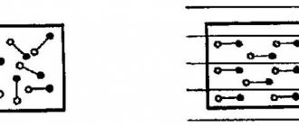
In a semiconductor, the atoms are arranged in a strict order: each atom is surrounded by four
the same atoms. Moreover, they are located so close to each other that their valence electrons form single orbits passing around neighboring atoms, thereby linking the atoms into a single whole substance.
Let us imagine the relationship of atoms in a semiconductor crystal in the form of a flat diagram. In the diagram, red balls with a plus symbol, conventionally, indicate atomic nuclei
(positive ions), and the blue balls are
valence electrons
.
Here you can see that around each atom there are four
exactly the same atoms, and each of these four has a connection with four other atoms, etc.
Each atom is bound to each neighboring atom by two
valence electrons, with one electron being its own and the other borrowed from the neighboring atom.
Such a bond is called two-electron or covalent
.
In turn, the outer layer of the electron shell of each atom contains eight
electrons:
four
of their own, and
one each
borrowed from four
neighboring
atoms.
Here you can no longer distinguish which of the valence electrons in the atom is “yours” and which is “foreign”, since they have become common. With such a connection of atoms in the entire mass of a germanium or silicon crystal, we can consider that the semiconductor crystal is one large molecule
. In the figure, pink and yellow circles show the connection between the outer layers of the shells of two neighboring atoms.
How molecules are made from atoms
Any atom is in a stable state if there are 8 electrons in its outer orbit. It does not seek to take electrons from neighboring atoms, but it does not give up its own. To verify the validity of this, it is enough to look at the inert gases in the periodic table: neon, argon, krypton, xenon. Each of them has 8 electrons in the outer orbit, which explains the reluctance of these gases to enter into any relationships (chemical reactions) with other atoms or to build molecules of chemical substances.
The situation is completely different for those atoms that do not have the coveted 8 electrons in their outer orbit. Such atoms prefer to unite with others in order to supplement their outer orbit with up to 8 electrons and achieve a calm, stable state.
For example, here is the well-known water molecule H2O. It consists of two hydrogen atoms and one oxygen atom, as shown in Fig. 1.
How a water molecule is created (Fig. 1)
At the top of the figure, two hydrogen atoms and one oxygen atom are shown separately. There are 6 electrons in the outer orbit of oxygen and two electrons in two hydrogen atoms nearby. Oxygen lacks just two electrons in its outer orbit to reach the coveted number 8, which it will receive by attaching two hydrogen atoms to itself.
Each hydrogen atom lacks 7 electrons in its outer orbit to be completely happy. The first hydrogen atom receives 6 electrons from oxygen into its outer orbit and one more electron from its twin, the second hydrogen atom. There are now 8 electrons in its outer orbit along with its electron. The second hydrogen atom also completes its outer orbit to the coveted number 8. This process is shown in the lower part of Fig. 1.
In Fig. Figure 2 shows the process of combining sodium and chlorine atoms. The result is sodium chloride, which is sold in stores under the name table salt.
The process of combining sodium and chlorine atoms (Fig. 2)
Here, too, each of the participants receives from the other the missing number of electrons: chlorine adds a single sodium electron to its own seven electrons, while it gives its own to the sodium atom. Both atoms have 8 electrons in the outer orbit, which ensures complete agreement and well-being.
Electrical conductivity of a semiconductor.
Consider a simplified drawing of a semiconductor crystal, where atoms are represented by a red ball with a plus, and interatomic bonds are shown by two lines symbolizing valence electrons.
At temperatures close to absolute zero, a semiconductor does not conduct
current, since there are no
free electrons
.
But with increasing temperature, the connection of valence electrons with atomic nuclei weakens
and some of the electrons, due to thermal movement, can leave their atoms.
An electron released from an interatomic bond becomes “ free
”, and where it was before, an empty space is formed, which is conventionally called
a hole
.
The higher
temperature of the semiconductor, the
more
free electrons and holes it becomes.
As a result, it turns out that the formation of a “hole” is associated with the departure of a valence electron from the shell of an atom, and the hole itself becomes a positive
electric charge equal to
the negative
charge of the electron.
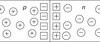
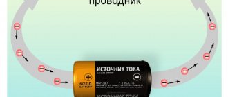
Now let's look at the figure, which schematically shows the phenomenon of current generation in a semiconductor
.
If you apply some voltage to the semiconductor, the “+” and “-” contacts, then a current will arise in it. Due to thermal phenomena
, in a semiconductor crystal, a certain number of electrons will begin
to be released
(blue balls with arrows).
Electrons, attracted by the positive
pole of the voltage source, will
move
towards it, leaving behind
holes
that will be filled with other
released electrons
.
That is, under the influence of an external electric field, charge carriers acquire a certain speed of directional movement and thereby create an electric current
.
For example: the released electron closest to the positive pole of the voltage source is attracted
this pole.
By breaking an interatomic bond and leaving it, an electron leaves
behind
a hole
.
Another released electron, which is located at some distance
from the positive pole, is also
attracted
by the pole and
moves
towards it, but
when it encounters
a hole on its way, it is attracted into it
by the nucleus
of the atom, restoring the interatomic bond.
The resulting new
the hole after the second electron
is filled by
the third released electron located next to this hole (Figure No. 1).
In turn, the holes
located closest to
the negative
pole are filled with other
released electrons
(Figure No. 2). Thus, an electric current arises in the semiconductor.
While there is an electric field
, this process
is continuous
: interatomic bonds are broken - free electrons appear - holes are formed. The holes are filled with released electrons - interatomic bonds are restored, while other interatomic bonds are broken, from which electrons leave and fill the next holes (Figure No. 2-4).
From this we conclude: electrons move from the negative pole of the voltage source to the positive, and holes move from the positive pole to the negative
.
Hole
This term has other meanings, see Hole (meanings).
| It is necessary to check the quality of the translation and bring the article into compliance with the stylistic rules of Wikipedia. You can help improve this article by correcting errors. Original in English - Electron hole. This mark has been on the article since May 1, 2012. |
| Hole | |
| Symbol: | h (English hole) |
| |
| Compound: | Quasiparticle |
| Classification: | Light holes, heavy holes |
| Named after whom and/or what: | Lack of electron |
| Quantum numbers: | |
| Electric charge: | +1 |
| Spin: | Determined by the spin of electrons in the valence band ħ |
A hole is a quasiparticle, a carrier of a positive charge equal to the elementary charge in semiconductors.
Definition according to GOST 22622-77: “An unfilled valence bond, which manifests itself as a positive charge, numerically equal to the charge of an electron.”
The concept of a hole is introduced in band theory to describe electronic phenomena in the valence band, which is not completely filled with electrons. In the electronic spectrum of the valence band, several zones often appear that differ in effective mass and energy position (zones of light and heavy holes, zone of spin-orbit split holes).
Electron-hole conductivity.
In a “pure” semiconductor crystal, the number of released
at a given moment, electrons are equal to the number of
formed
in this case, therefore the electrical conductivity of such a semiconductor
is small
, since it provides
great
resistance to the electric current, and such electrical conductivity is called
intrinsic
.
But if you add it to a semiconductor as an impurity
a certain number of atoms of other elements, then its electrical conductivity will increase several times, and depending on
the structure
of the atoms of impurity elements, the electrical conductivity of the semiconductor will be
electronic
or
hole
.
Electronic conductivity.
Let's say that in a semiconductor crystal in which the atoms have four valence electrons, we replace one atom with an atom that has five
valence electrons.
This atom with its four
electrons will bond with four neighboring atoms of the semiconductor, and
the fifth
valence electron will remain “
extra
” - that is, free.
And the more
such atoms there are in the crystal, the
more
free electrons there will be, which means that such a semiconductor in its properties will approach the metal, and in order for an electric current to pass through it,
interatomic bonds in it do not necessarily have to be destroyed
.
n” type semiconductors
", or
n
-type semiconductors.
Here the Latin letter n comes from the word “negative” - that is, “negative”. It follows that in an n
-type
the main
charge carriers are
electrons
, and not the main ones are holes.
Impurities and defects in semiconductors
Electric P.'s conductivity can be caused both by the electrons of the own atoms of a given substance (intrinsic conductivity) and by the electrons and holes of impurity atoms (impurity conductivity). The process of introducing impurities into P. to obtain the necessary physical properties. properties is called doping of semiconductors. Since the binding energy of charge carriers in impurity atoms ranges from several meV to several tens of meV, it is impurity conductivity that explains the exponential increase in the concentration of free charge carriers in most atoms in the temperature range near room temperature.
Impurities are usually introduced into polymers during the growth of the structure; they can be donors or acceptors, that is, suppliers of electrons or holes. If, for example, impurity atoms of group V elements (As, P) are introduced into germanium Ge or silicon Si (elements of group IV), then the 4 outer electrons of these atoms form a stable bond with four neighboring atoms of the lattice, and the fifth electron will be unbound and will be held near the impurity atom only due to the Coulomb interaction, weakened by the dielectric. polarization of the environment. Such an impurity atom is a donor and is easily ionized at room temperature. An acceptor appears, for example, when Group III elements (Ga, Al) are introduced into Ge or Si. In this case, to form all four bonds with the nearest atoms, an addition is required. electron, which is taken from the internal shells of atoms, so that the impurity atom is negatively charged. Electroneutrality is restored due to the fact that internal the unfilled orbital is distributed near neighboring atoms of the lattice, located from the impurity at distances exceeding the interatomic distance. The presence of donors or acceptors leads to n- or p-type conductivity, respectively.
Particles in which acceptor and donor impurities can simultaneously exist are called compensated. Compensation for impurities leads to the fact that part of the electrons from donors goes to acceptors, and as a result, the result appears. concentration of ions that effectively influence the conductivity of semiconductors.
The amplitude of the wave function of electrons or holes localized on impurity atoms is 1–10 nm. This means that at a concentration of impurity atoms of approx. 1018 cm–3, the wave functions of electrons and holes of neighboring atoms begin to overlap, charge carriers can move from ion to ion, and the electron becomes degenerate (see Degenerate semiconductors). Such P. are called heavily alloyed. Due to the strong screening of Coulomb attraction, the charge carriers in them are free even at such low temperatures at which thermal interaction was impossible. activation of an electron or hole from an isolated atom.
In the absence of external electrical field or illumination, the concentration of free charge carriers is called equilibrium and is determined by the width of the band gap, the effective masses of charge carriers, the concentration of impurities, and the binding energy of impurity charge carriers.
Along with impurities, sources of charge carriers can also be various. structural defects, e.g. vacancies (the absence of one of the lattice atoms), interstitial atoms, as well as a deficiency or excess of atoms of one of the components in semiconductor compounds (deviations from the stoichiometric composition).