Power conversion technology
pn (pe-en) junction is a region of space at the junction of two p- and n-type semiconductors, in which a transition from one type of conductivity to another occurs, such a transition is also called an electron-hole transition.
There are two types of semiconductors: p and n types. In the n type, the main charge carriers are electrons , and in the p type, the main charge carriers are positively charged holes. A positive hole appears after an electron is removed from an atom and a positive hole is formed in its place.
To understand how a pn junction works, you need to study its components, that is, a p-type and n-type semiconductor.
P and n type semiconductors are made on the basis of monocrystalline silicon, which has a very high degree of purity, so the slightest impurities (less than 0.001%) significantly change its electrical properties.
In an n-type semiconductor, the main charge carriers are electrons . To obtain them, donor impurities that are introduced into silicon - phosphorus, antimony, arsenic.
In a p-type semiconductor, the majority charge carriers are positively charged holes . To obtain them, acceptor impurities - aluminum, boron.
Atoms and covalent bond
First, let's understand at the atomic level what and how it works. This will be a short introduction.
All matter is made up of molecules, and molecules in turn are made up of atoms. And every atom has protons, neutrons and electrons.
Protons and neutrons form a nucleus in which there are equal numbers of them.
The exception is hydrogen, which has only one proton in its nucleus, without a neutron.
There are orbits of electrons around the nucleus (by the way, it is now generally accepted that this is a cloud of electrons). Between them there are strong and weak forces, which are the basis of atoms. Further, we will not indicate protons and neutrons in the images for ease of perception.
Of course, one can delve further into the fact that there are mesons, quarks and other fundamental particles. And also that on the electronic shells of atoms, electrons are distributed in the form of a “gas” and they cannot be accurately detected, only with a certain degree of probability. However, this is not necessary to understand the operating principles of general digital electronics.
It is enough to simply accept the fact that there are atoms that have nuclei with a positive charge, and around this nucleus there are orbits with electrons.
Electrons and protons have opposite signs.
An electrically neutral atom has the same number of electrons and protons. All electrons are distributed over different levels. Those closest to the nucleus have two electrons, the next level has 4 electrons, and so on. But if for any reason an atom loses an electron, then that atom becomes a positive ion.
It lacks an electron in its outer electron orbital, which is called the valence level. It is easier to “take away” an electron from the valence level of an atom. And such electrons that are at the valence level are called valence electrons.
A positive ion (an atom that is deficient in electrons) will have a + sign because it is deficient in electrons and will attract or be attracted to a free electron (depending on the environment).
All atoms in molecules are connected to each other at the valence level, that is, using a covalent bond.
At the valence level, the bond between the nucleus and electrons is much smaller than at others, so atoms can form matter by combining with other atoms. This is how chemical reactions and atoms combine with each other.
Reverse current
The reverse current in a diode consists of the minority carrier current and the surface leakage current. This reverse current is so small that you can't even notice it and it is considered almost zero.
Reverse saturation current
As is known, thermal energy continuously creates pairs of free electrons and holes. Suppose that thermal energy created a free electron and a hole inside the depletion region.
The depletion region pushes the newly created free electron into the n region, causing it to leave the right end of the diode. When it reaches the right end of the diode, it enters the outer wire and flows to the positive terminal of the battery.
On the other hand, the newly created hole is placed in the region p. This extra hole on the p side allows one electron from the negative terminal of the battery to enter the left end of the diode and fall into the hole.
Because thermal energy continuously creates electron-hole pairs within the depletion region, a small continuous current flows in the external circuit. This reverse current, caused by thermally generated minority carriers, is called saturation current . The name saturation means that increasing the reverse voltage will not increase the amount of thermally produced minority carriers.
Surface leakage current
A different current exists in a reverse biased diode. A small current flows across the surface of the crystal, known as surface leakage current .
The atoms on the top and bottom surfaces of the crystal have no neighbors. They have only six electrons in their valence orbital. This means that each surface atom has two holes. The following image shows these holes along the surface of the crystal.
Because of this, electrons pass through surface holes from the negative terminal of the battery to the positive terminal of the battery. Thus, a small reverse current flows along the surface.
Semiconductors and crystal lattice
Now we smoothly move on to semiconductors. Semiconductors such as silicon (Si) and germanium (Ge) each have 4 electrons at the covalent level.
Don't confuse flint and flint. Flint is a mineral and silicon is a chemical element that was discovered in 1810.
The peculiarity of semiconductors is that their atoms form pair bonds with each other.
Let's say there is a silicon atom. It has 4 electrons in its valence level. If you add 4 more silicon atoms to it, you get a crystal lattice. 4 atoms are connected to each other by their 4 electrons.
The picture shows the connection of atoms in a plane. In reality, it is naturally located not in one plane, but in space.
That is, each atom can form a stable bond with each other, 4 pieces on each side and plane.
The peculiarity of semiconductors is that this crystal lattice is very stable.
By the way, the conductivity of semiconductors strongly depends on external conditions (pressure, temperature, radiation, light). Much stronger than other materials. This is all due to the peculiarity of the crystal lattice, which will make it possible to make solar panels, sensors, cameras and much more.
So, atoms of semiconductors without impurities are electrically neutral.
And most importantly, they will still be connected to each other. A common covalent bond will allow them to exchange electrons with each other.
The conductivity of semiconductors under normal conditions is almost the same as that of dielectrics, that is, very low.
Reverse bias region
The reverse bias region exists between zero current and breakdown.
In this region, a small reverse current flows through the diode. This reverse current is caused by thermally produced minority carriers. This reverse current is so small that you can't even notice it and it is considered almost zero.
Conductivity of a crystal lattice with impurities
There are few free electrons in a pure semiconductor, and this explains the low conductivity of the material.
However, as the temperature increases, the electrons at the valence level gain more energy and can leave their orbits faster. Therefore, the material becomes more conductive as the temperature increases.
And because of this, semiconductors got their name. This is both a conductor and a dielectric in one bottle, which changes its conductivity due to external conditions.
Donor admixture and n-type
If you add an atom with 5 valence electrons to the silicon crystal lattice, then free electrons will appear in the crystal.
For example, there is an arsenic atom (As) and silicon atoms (Si).
The 4 valence electrons of arsenic form a valence bond with other silicon atoms. But one electron will be in the conduction band. That is, it will become a free electron.
But the arsenic atom, which unintentionally gave up its electron, will become a positive ion. And despite this, the crystal lattice remains stable.
A doped semiconductor containing free electrons is called an n-type semiconductor. The main charge carriers are free electrons. Minor ones are holes.
Impurities are added through doping. It can be either metallurgical (increased temperature, production of alloys) or chemical (ionic and diffuse).
If a current is applied through such a material, free electrons from the impurity are attracted by a positive potential. And from the negative potential “new” electrons come, replacing the old ones that went to the positive potential.
Acceptor impurity and p-type
What happens if an atom with three valence electrons, for example boron (B), is added to a semiconductor?
Then the three valence electrons of the boron atom will create a bond with other silicon atoms. However, now a crystal with such an impurity will be missing one electron.
This absence of an electron is called a hole. In essence, this is a positive potential, but for ease of understanding it is usually called a hole.
It is not an ion or an elementary particle. This is an electron deficiency in atoms. And the atom that lacks an electron in its orbit will attract both free electrons that are in the crystal and electrons from neighboring atoms.
Such an impurity in the crystal also increases its conductivity. And this impurity is called acceptor. That is, impurity atoms create a deficiency of electrons in the crystal lattice.
Therefore, such a semiconductor with an acceptor impurity is called p-type. Its main charge carriers are holes. And the minority ones are electrons.
If you pass a current through such a material, then the hole will be attracted to the negative potential towards the new incoming electron from the current source. But the electrons that were in the crystal will go to the positive potential.
By the way, an impurity boron atom turns out to be a negatively charged ion, since when a current passes in its orbit there will be not 3 electrons, but 4, which is an excess for it.
Current of minor charges
As mentioned above, in the p-type the main charge carriers are holes, and in the n-type they are electrons. Minor carriers are, accordingly, the opposite. And minority charge carriers also participate in the passage of current.
Of course, there are much fewer minority charge carriers than majority charge carriers, but you should not completely ignore them, especially when it comes to pn junctions.
Equilibrium (zero displacement)
In a PN junction without an externally applied voltage, the equilibrium condition is achieved. Let's see how.
Depletion area
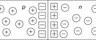
An n-type semiconductor has more free electrons than a p-type semiconductor. Because of this high concentration of electrons on the n-side, they repel each other.
Due to repulsion, free electrons spread (scatter) in all directions. Some of them cross the border between n and p. When a free electron enters the p region, it is attracted to the positive hole and recombines with it. When this happens, the hole disappears and the free electron becomes a valence electron.
When a free electron falls into a hole on the p-side, the p-side atom gains an extra electron. An atom that gains an extra electron has more electrons than protons, making it a negative ion.
Likewise, every free electron that leaves an n-side atom creates a hole in the n-side atom. An atom that loses an electron has more protons than electrons, making it a positive ion.
Thus, each time an electron crosses a junction and recombines with a hole, it creates a pair of ions. The following figure shows these ions on each side of the connection.
Each pair of positive and negative ions at the junction is called a dipole . Creating a dipole means that one free electron on the n-side and one hole on the p-side are removed from circulation. As the number of dipoles increases, the region near the transition becomes depleted of majority charge carriers. Therefore we call this uncharged region the depletion .
Barrier potential
Each dipole has an electric field between positive and negative ions. Whenever a free electron tries to enter the depletion region, this electric field pushes it back into the n region.
The electric field strength increases with each electron-hole recombination within the depletion region. Therefore, the electric field eventually stops the diffusion of electrons through the junction and equilibrium is achieved.
The electric field between ions is equivalent to a potential difference called the barrier potential . At room temperature, the barrier potential is approximately 0.3 V for germanium diodes and 0.7 V for silicon diodes.
Creating a pn junction
What happens if you combine two pieces of silicon with p-type and n-type impurities together? The result is a pn junction. Or as it is also called - electron-hole transition.
This transition is the demarcation zone between the p-region and the n-region.
And the peculiarity of this transition is that this transition consists of ionized impurity atoms, which do not allow free charges from two different regions to connect with each other. It was formed from such a phenomenon as diffusion current.
This current occurs during heating (making the junction). Charge carriers recombine with each other and balance the balance. The diffusion current under the influence of heat is chaotic and does not have an ordered direction unless it is acted upon by external voltage.
For example, electrons from the n-region begin to accumulate near the positive ions of the impurity, but since there are negative ions of the n-region on the other side, they cannot cross this barrier. The situation with holes is similar.
Free electrons from the n-region cannot move to the p-region due to the barrier created by ionized donor impurities. This creates an electric field that acts as a barrier to holes and electrons. And because of this, there are no free charge carriers in the pn junction. The transition simply pushes them away from both sides.
By the way, another name for the barrier is the depleted region.
In general, the crystal remains electrically neutral. If this barrier did not exist, the free charge carriers would balance each other.
Overcoming a Potential Barrier
In order for free electrons and holes to pass through this barrier, an external voltage must be applied that will exceed the voltage required to cross the barrier.
Let's connect the minus of the current source to the n-region, and the plus of the current source to the p-region. This inclusion is called direct. In devices, the n-region is also called the cathode, and the p-region is called the anode.
The source voltage must be higher than that required to open the pn junction.
Let's say the potential barrier is 0.125 Volts. To overcome it, we connect a source with a voltage of 5 V.
In order not to overload the perception, the diagram does not show minority charge carriers.
And thanks to the influence of the electric field of an external source, free carriers have enough energy to cross this potential barrier and overcome its electric field. The junction is connected with forward bias.
A fresh electron comes from the source, goes to the n-region, then overcomes the barrier and goes to the hole, where recombination occurs. And then this electron goes to meet the hole, which comes from a positive potential connected to the p-region. That is, an electric current passes through the pn junction. This current is also called diffusion current or direct current - when the main charge carriers move in an orderly manner to an external current source.
The situation is similar with holes. The positive potential of an external source, which is connected to the p-region, will take away an electron, and a hole will appear in its place. The hole, in turn, will move towards the barrier and further towards the negative potential of the source.
The current that is created by holes is called hole current. Accordingly, the current that is created by electrons is electronic.
And in this diagram the transition is shown without a barrier, but with reverse current.
Minority charge carriers, in turn, act in the opposite way, which causes additional resistance in the pn junction.
The reverse current can be as small as a few microamps.
Reverse switching
Let's change the polarity of the external source to the opposite. Minus to the p-region, and plus to the n-region. What will happen to the barrier and the charge current?
The barrier will increase due to the fact that the main charge carriers will be attracted to an external source. The resistance of the potential barrier and its opening voltage will increase.
However, despite all this, reverse current will flow through the pn junction.
This reverse current is very small because it is generated by minority charge carriers. It is also called drift current.
Reverse bias
Connecting p-type to the negative terminal of the battery and n-type to the positive terminal corresponds to reverse bias. The following figure shows a reverse biased diode.
The negative terminal of the battery attracts holes, and the positive terminal of the battery attracts free electrons. This causes holes and free electrons to flow out of the junction, leaving positive and negative ions behind. Consequently, the depletion area becomes wider.
The width of the depletion region is proportional to the reverse voltage. As the reverse voltage increases, the depletion region becomes wider. The depletion region stops growing when its potential difference is equal to the applied reverse voltage. When this happens, electrons and holes stop moving away from the connection.
Application of pn junction
This is how a simple diode works, which consists of a pn junction. Simply put, a pn junction is a classic diode. And it can work both with direct connection and with reverse connection. In general, all modern digital technology consists of pn junctions.
Transistors, thyristors, microcircuits, logic elements, processors and much more are based on this.
Controlled avalanche breakdown
What happens if the voltage of the potential barrier is exceeded? For example, it is equal to 7 V. And in the diagram the source is 5 V. If we connect a source to 8 V, then an avalanche-like current will occur.
Minority charge carriers will take the majority ones with them. This process is partly controlled if we do not exceed the source voltage higher than the pn junction can withstand.
Electrical breakdown
If we increase the voltage even more, there will be an electrical breakdown. These phenomena are widely used in practice, for example, as stabilizers.
The current will not flow through the circuit until there is the voltage required to open the reverse biased pn junction.
And the electrical breakdown is controlled. Zener diodes (the so-called diodes that operate in this mode) are made specifically with wide pn junctions that operate for a long time under constant loads.
Thermal breakdown
But if the radio component is not initially designed for electrical breakdown, then it will quickly heat up and a thermal breakdown will occur. The holes and electrons will receive thermal energy, due to which the barrier will completely collapse. The junction heats up and cracks under the influence of temperature. This is an irreversible process.
In general, when equipment “burns out”, this is the phenomenon of thermal breakdown, that is, exceeding the permissible temperature.
And during soldering, thermal breakdown can also occur. It is enough to overheat the part a little and the pn junction will be destroyed.
Accordingly, if you pass a current through the diode that exceeds its capacity, then thermal breakdown will also occur. The same applies to power dissipation.
Rectifier diodes
Structurally, rectifier diodes are divided into planar and point diodes, and according to manufacturing technology into alloy, diffusion and epitaxial. Due to their large pn junction area, planar diodes are used to rectify large currents
.
Point diodes have a small transition area and, accordingly, are designed to rectify small currents
. To increase the avalanche breakdown voltage, rectifier columns are used, consisting of a series of diodes connected in series.
High power rectifier diodes are called power diodes
. The material for such diodes is usually silicon or gallium arsenide. Silicon alloy diodes are used to rectify alternating current with a frequency of up to 5 kHz. Silicon diffusion diodes can operate at higher frequencies, up to 100 kHz. Silicon epitaxial diodes with a metal substrate (with a Schottky barrier) can be used at frequencies up to 500 kHz. Gallium arsenide diodes are capable of operating in the frequency range up to several MHz.
Power diodes are usually characterized by a set of static and dynamic parameters. To static parameters
diodes include:
- voltage drop
Upr across the diode at a certain value of forward current; - reverse current
Irev at a certain value of reverse voltage; - average value of forward current
Ipr.av; - pulse reverse voltage
Urev.i.;
To dynamic parameters
diode include its time and frequency characteristics. These parameters include:
reverse voltage recovery time-
current rise time - maximum frequency
without reducing diode modes fmax.
Static parameters can be set using the current-voltage characteristic of the diode.
The diode reverse recovery time tres is the main parameter of rectifier diodes, characterizing their inertial properties. It is determined when the diode switches from a given forward current Ipr to a given reverse voltage Urev. During switching, the voltage across the diode becomes reversed. Due to the inertia of the diffusion process, the current in the diode does not stop instantly, but over time tout. Essentially, charge resorption occurs at the boundary of the pn junction (i.e., discharge of equivalent capacity). It follows from this that the power loss in the diode increases sharply when it is turned on, especially when turned off. Therefore, the losses in the diode
increase with increasing frequency of the rectified voltage.
When the temperature of the diode changes, its parameters change. The forward voltage on the diode and its reverse current depend most strongly on temperature. Approximately, we can assume that TKN (temperature coefficient of voltage) Upr = -2 mV/K, and the reverse current of the diode has a positive coefficient. So, with every 10 °C increase in temperature, the reverse current of germanium diodes increases by 2 times, and of silicon diodes by 2.5 times.
How else is reverse inclusion used?
Also, reverse switching is very similar to a capacitor. Take a look at the diagram. These are two plates of a capacitor, in the middle of which there is a “dielectric”. And the electron-hole junction has a capacitance. And this is also used in practice. This is the name of a semiconductor capacitor.
In radio receivers, varicaps are used instead of interlinear capacitors. Varicaps are easy to set up. You just need to apply a reverse bias voltage of a certain value to increase or decrease the capacitance.
Of course, this is not the main application of a pn junction. Transition is used in different ways throughout digital technology.
Rectifiers, amplifiers, generators, processors, solar panels and much more. And what was described above about the operating principle of a pn junction is the operating principle of a conventional diode.
Designation and determination of the main electrical parameters of diodes
Designation of a semiconductor diode
As mentioned earlier, a diode conducts current in one direction (i.e., it is ideally just a conductor with low resistance), in the other direction it does not (i.e., it turns into a conductor with a very high resistance), in a word, it has one-way conductivity
.
Accordingly, it has only two conclusions. As has been the custom since the times of lamp technology, they are called anode
(positive terminal) and
cathode
(negative).
All semiconductor diodes can be divided into two groups: rectifier and special. Rectifier diodes
, as the name suggests, are designed to rectify alternating current.
Depending on the frequency and shape of the alternating voltage, they are divided into high-frequency, low-frequency and pulsed. Special
types of semiconductor diodes use different properties of pn junctions; breakdown phenomenon, barrier capacitance, presence of areas with negative resistance, etc.