Characterization and Definition of Semiconductors
In the periodic table, 25 chemical elements are non-metals, of which 13 elements have semiconducting properties. The main difference between semiconductors and other elements is that their electrical conductivity increases significantly with increasing temperature.
Another feature of a semiconductor is that its resistance drops when exposed to light. Moreover, the electrical conductivity of semiconductors changes when a small amount of impurity is added to the composition.
Semiconductors can be found among chemical compounds with a variety of crystal structures. For example, elements such as silicon and selenium, or binary compounds like gallium arsenide.
Semiconductor materials can also include many organic compounds, for example polyacetylene (CH)n. Semiconductors can exhibit magnetic (Cd1-xMnxTe) or ferroelectric properties (SbSI). With sufficient doping, some become superconductors (SrTiO3 and GeTe).
A semiconductor can be defined as a material with an electrical resistance between 10-4 and 107 ohm m. The following definition is also possible: the band gap of a semiconductor should be from 0 to 3 eV.
Energy gap
The valence orbitals of atoms in a crystal lattice are divided into two groups of energy levels - the free band, located at the highest level and determining the electrical conductivity of semiconductors, and the valence band, located below. These levels, depending on the symmetry of the crystal lattice and the composition of the atoms, can intersect or be located at a distance from each other. In the latter case, an energy gap or, in other words, a forbidden zone appears between the zones.
The location and filling of the levels determines the electrical conductivity properties of the substance. Based on this criterion, substances are divided into conductors, insulators and semiconductors. The band gap of the semiconductor varies in the range of 0.01–3 eV, and the energy gap of the dielectric exceeds 3 eV. Metals do not have energy gaps due to the overlap of levels.
Semiconductors and dielectrics, as opposed to metals, have a valence band filled with electrons, and the nearest free band, or conduction band, is fenced off from the valence band by an energy gap - a region of forbidden electron energies.
In dielectrics, thermal energy or a small electric field is not enough to make a jump through this gap; electrons do not enter the conduction band. They are not able to move along the crystal lattice and become carriers of electric current.
To initiate electrical conductivity, an electron at the valence level must be given energy that would be sufficient to overcome the energy gap. Only by absorbing an amount of energy no less than the size of the energy gap will the electron move from the valence level to the conduction level.
If the width of the energy gap exceeds 4 eV, excitation of the conductivity of the semiconductor by irradiation or heating is practically impossible - the excitation energy of electrons at the melting temperature is insufficient to jump through the energy gap zone. When heated, the crystal will melt until electronic conduction occurs. Such substances include quartz (dE = 5.2 eV), diamond (dE = 5.1 eV), and many salts.
Electronic conductivity
Although electrons are “common to the crystal,” if their energy is low, then their mobility is limited only by electron orbits; they are not free and cannot conduct electric current.
As the temperature of the substance increases, the energy of the electrons also increases, and it begins to be sufficient to leave the electron orbit and break the covalent bond.
In this case, the electron finds itself in the space between the ions, outside of “its” orbit, and can move under the influence of an external electric field - it becomes a free carrier. As the temperature increases, there are more and more such carrier electrons, and the conductivity of the crystal increases.
The described mechanism is called electronic conductivity of a semiconductor.
Characteristics of semiconductors
Of the 104 elements of the periodic table, 79 are metals, 25 are non-metals, of which 13 chemical elements have semiconductor properties and 12 have dielectric properties. The main difference between semiconductors is that their electrical conductivity increases significantly with increasing temperature. At low temperatures they behave like dielectrics, and at high temperatures they behave like conductors. This is how semiconductors differ from metals: the resistance of a metal increases in proportion to the increase in temperature.
Another difference between a semiconductor and a metal is that the resistance of a semiconductor drops under the influence of light, while the latter does not affect a metal. The conductivity of semiconductors also changes when a small amount of impurity is introduced.
Semiconductors are found among chemical compounds with a variety of crystal structures. These can be elements such as silicon and selenium, or binary compounds such as gallium arsenide. Many organic compounds, such as polyacetylene (CH)n, are semiconductor materials. Some semiconductors exhibit magnetic (Cd1-xMnxTe) or ferroelectric properties (SbSI). Others, when sufficiently doped, become superconductors (GeTe and SrTiO3). Many of the recently discovered high-temperature superconductors have non-metallic semiconducting phases. For example, La2CuO4 is a semiconductor, but when formed into an alloy with Sr it becomes a superconductor (La1-xSrx)2CuO4.
Physics textbooks define a semiconductor as a material with an electrical resistance from 10-4 to 107 Ohm m. An alternative definition is also possible. The band gap of the semiconductor is from 0 to 3 eV. Metals and semimetals are materials with zero energy gap, and substances in which it exceeds 3 eV are called insulators. There are exceptions. For example, semiconductor diamond has a bandgap width of 6 eV, semi-insulating GaAs - 1.5 eV. GaN, a material for optoelectronic devices in the blue region, has a band gap of 3.5 eV.
Semiconductor Doping
Semiconductor Doping
is the process of introducing impurities or structural defects with the aim of purposefully changing electrical properties.
The electrical properties of doped semiconductors depend on the nature and concentration of the introduced donor or acceptor impurities. Impurities, as a rule, form substitutional solid solutions in semiconductors and have high solubility up to values of 1018 – 1020 cm–3. These impurities have small carrier capture cross sections, are ineffective recombination centers, and have virtually no effect on the lifetime of charge carriers.
Doping methods are divided into two groups: either directly in the processes of growing single crystals and epitaxial structures, or local doping of individual areas of single crystals.
In Fig. 1.19 shows the classification of semiconductor doping methods. Let us give a brief analysis of these methods.
High temperature alloying
High temperature diffusion method
consists in the fact that the dopant is brought into contact with the surface of a single crystal of silicon. The single crystal heats up, and impurity atoms penetrate inside the single crystal, replacing silicon atoms in the lattice.
The high-temperature diffusion method is one of the most developed and widely used processes for creating local regions with a given type of conductivity in semiconductors.
Rice. 1.19. Classification of local doping methods for semiconductors
There are several mechanisms for introducing impurities.
With diffusion of substitution
(diffusion along vacancies) the lattice experiences strong thermal vibration when heated. Some atoms leave their places and are replaced by others. If an impurity atom with approximately the same size and valency happens to be nearby, then the missing atom at a lattice site may be replaced by an impurity atom. Impurity atoms move stochastically along lattice sites in all directions, but in general their movement is directed towards decreasing the impurity concentration. The rate of substitution diffusion depends on the rate of formation of vacancies in the lattice.
With diffusion of implantation
the impurity atom finds a place in the crystal lattice in the interstices, without replacing the atom of the original element. At high temperatures, impurity atoms can jump from one interstitial site to another, spreading at a higher speed than with substitutional diffusion.
To manufacture barriers and p–n junctions, the process of diffusion of impurity atoms is used, which are introduced into the crystal lattice of the semiconductor and change its electrical properties.
The process of isotropic diffusion is described using the diffusion coefficient D
and is determined from
Fick’s first law:
where j
– flux density of diffusing atoms,
N
– concentration of atoms,
x
– coordinate.
This phenomenological law was formulated in 1855 by A. Fick by analogy with the heat equation.
Diffusion coefficient D
depends on temperature
T
as follows:
where D
0 is a constant value, ε is the activation energy for an atomic jump,
k
is Boltzmann’s constant.
The change in the concentration of a diffusing substance over time during one-dimensional diffusion is determined by Fick’s second law:
The dopant in a semiconductor can be introduced from a gaseous, liquid or solid source. Therefore, according to the method of introducing an impurity from an external source to the medium in which it is necessary to create inhomogeneities in the concentration of impurities, three methods are distinguished.
During diffusion in a closed system
("closed pipe" method), conductor plates and sources of impurities (diffusant) are loaded into a quartz ampoule, evacuated, sealed and placed in an oven (Fig. 1.20,
a
). Substances in any state of aggregation can be used as a diffusant. The closed pipe is first heated to the decomposition temperature of the gaseous source. A local diffusion source is formed on the alloyed plates, the location of which is determined by the corresponding mask. Then the temperature rises, which creates the necessary conditions for the diffusion of the dopant in the bulk of the semiconductor. As a result, regions with a given impurity concentration and a given type of conductivity are formed. The method has a number of disadvantages:
– the electrical parameters of the doped areas significantly depend on the composition of the atmosphere in the isolated working volume;
– a two-stage heat treatment process increases the duration of the alloying process;
– preparing a closed pipe requires a lot of time;
– obtaining a sample is accompanied by destruction of the pipe;
– low reproducibility of electrophysical parameters at low surface impurity concentration.
Rice. 1.20. Diagram of diffusion methods: 1
– open diffusion pipe;
2
– closed diffusion pipe;
3
– plates;
4
– hood;
5
– output end for introducing carrier gas;
6
– diffusion furnace;
7
– ampoules with diffusant;
8
– solid diffuser;
9
– liquid diffuser
Most often, this method is used for the purpose of deep alloying.
The most widely used method is diffusion in an open system.
("open pipe" method).
Diffusion in this case can be carried out from solid, liquid or gaseous sources. The main diffusants during diffusion into silicon are boron and phosphorus. The creation of local heterogeneities is carried out in two stages. At the first stage (the driving stage),
a thin diffusion layer of impurity is created in the required places on the surface at temperatures that are low compared to diffusion.
At the second stage (acceleration stage),
the plates are heated in an atmosphere that does not contain diffusants. In this case, a diffusion redistribution of impurities occurs, leading to the creation of a local region in the volume of the plate.
The two-step diffusion in this method has two main advantages. First, dividing the process into two stages makes the process more controllable, increases reproducibility of results and simplifies control. Secondly, the low-temperature process of the driving stage makes it easier to mask future static inhomogeneities. The acceleration stage occurs in the absence of diffusant vapor.
High temperature diffusion
possible using solid planar dopant sources. There are several ways to use solid sources. The most attractive is the location of the impurity source in parallel between the doped semiconductor wafers. The distance between the plates and the diffuser is determined by the relation
where D
is the diffusion coefficient of the impurity in a gaseous medium,
t
is the processing time of the plates.
Typically, the value of L
(diffusant plate) is selected close to the size of the semiconductor wafers, and the material is a glass-ceramic composition using boron oxide (B2O3), boron nitride (BN), and aluminum phosphate (Al2O3 3P2O5).
The use of solid planar sources makes it possible to improve the uniformity of doping, increase the percentage of yield of suitable structures, rationally use the working volume of a diffusion furnace, eliminate toxic reaction products, etc.
The method of high-temperature diffusion from the solid phase also makes it possible to reduce the duration of high-temperature treatment by 2–4 times, introduce donor and acceptor impurities simultaneously, and reduce the labor intensity of the doping operation by 2–3 times while simultaneously improving the electrical parameters of structures.
The solution to Fick's second law for given initial and boundary conditions has the form:
where N
(
x , t
) – concentration of impurities at a distance
x
from the surface,
N
– surface concentration of impurities,
t
– diffusion time.
The formation of transistor regions occurs by setting the concentration and time parameters of the diffusion process.
In Fig. 1.21 shows the calculated curves (a)
and the resulting impurity distribution profile
(b)
in the regions of the bipolar transistor.
Rice. 1.21. Formation of transistor bipolar structure regions by high-temperature diffusion
Summarizing the analysis of high-temperature diffusion methods, we note that these technological processes ensure the creation of local inhomogeneities in semiconductor continuum media in the form of regions with a wide range of concentrations and depths of impurities.
At the same time, high-temperature diffusion methods have a number of disadvantages: – isotropy, which leads to a limitation in the size of the formed inhomogeneity in the silicon wafer;
– changes in electrical characteristics, as well as the generation of dislocations and mechanical stresses in a continuum medium due to the processing of plates at high temperatures;
– a limited set of diffusants, in the temperature range 900 – 1250 °C, with a high diffusion coefficient and good solubility;
– the appearance of used impurities in the active region during the formation of the structure due to the flow of carrier gases or gases from the environment penetrating through the pipes;
– difficulty in obtaining thin doped layers and rare p–n junctions.
All this reduces the effectiveness of high-temperature diffusion methods and complicates highly efficient automation and integration of the entire technological process. Therefore, research work in the field of technology for creating areas of given conductivity and concentration is aimed at increasing the efficiency of processes and the rational combination of these processes with other doping methods.
Ion implantation
Ion implantation
(ion implantation, ion doping) is the process of introducing impurity atoms into a solid by bombarding its surface with accelerated ions.
In practice, the ion implantation method consists of bombarding solids with beams of accelerated ions with energies ranging from 10 keV to 1 MeV in order to create local inhomogeneities and p–n junctions in them. Accelerated ions penetrate the crystal lattice, overcoming the repulsive opposition of the positively charged nuclei of atoms. Ions of lighter substances penetrate deeper than ions of heavy substances, but the trajectory of the latter is more straightforward.
The depth of penetration of ions into a medium is characterized by the concept of range. Average normal mileage X
represents the projection of the trajectory of the average total path onto the direction of the initial velocity of the ion.
When the direction of incidence of the ion beam is precisely oriented along the crystallographic axis, the ions in the crystal are kaialized
. In this case, the ion range is significantly greater than with non-oriented irradiation. The ion can cause disorder zones in the lattice, the size of which can be 3 – 10 nm. This occurs when the energy transferred by an ion to an atom in the lattice exceeds the binding energy of the atoms in the solid. Disordered zones or radiation defects accumulate during irradiation, and when their number exceeds a critical value, a local transition of the crystalline structure into an amorphous layer occurs. Most of the interstitial ions are located in interstices and are not electrically active. To restore the crystal structure, the irradiated medium is annealed, resulting in the decay of radiation defects. At the same time, impurity ions occupy vacant sites and are introduced, forming regions with a given impurity concentration or p–n junctions. The design of the installation for ion implantation is shown in Fig. 1.22.
Rice. 1.22. Ion implantation installation diagram: 1
– ion source;
2 – pulling electrodes; 3 – channel; 4
– magnetic separator;
5
– focusing and scanning system;
6
– damper;
7
– accelerating tube;
8
– high voltage source;
9
– receiving chamber;
10
– drum;
11
– cylinder with leak
The source of ions is a gas-discharge chamber, in which the molecules and atoms of the implanted substance are ionized using electron bombardment. Additional ionization is carried out using a magnetic separator. Typically two or more dopant ion sources are used to produce p- and n-type regions. For example, boron trifluoride (BF3) coming from a cylinder with a leak is used as a source of acceptor impurity. Phosphorus vapor generated in a heater with red phosphorus is often used as a donor impurity. The ions are simulated using extraction electrodes connected to a high voltage source. The ion beam is formed in the channel using a magnetic separator and focusing and scanning systems. After passing through a magnetic separator, in which ions are selected by mass, they enter the focusing system.
The formed ion beam scans a surface located in a vertical plane. The shutter in the channel is designed to block the ion beam when a given radiation dose is reached. An acceleration tube with a high voltage source (~200 kV) is designed to accelerate the ions to the desired energy. The irradiated material is placed in a drum-type cassette located in the receiving chamber, which is evacuated to a level of 10–3 Pa.
Uniformity of doping is structurally ensured by rotating the drum and scanning the ion beam at a given irradiation time t
(c), determined from the relation
where α is the sector angle of the irradiated drum circumference; Q
– radiation dose, C/m2;
j
is the ion current density in the beam, A/m2.
The radiation dose determines the number of particles embedded in a unit surface:
where q
– charge of one ion,
n
– ionization multiplicity,
e
– electron charge.
A distinctive feature of the ion implantation method is the ability to create maximum concentration not on the surface, which was typical for diffusion processes, but in the depths of the medium. This happens because as the ion energy increases, the concentration maximum is located deep in the semiconductor. The surface concentration decreases. As the ion energy increases to 2.5 MeV, the penetration depth increases. In this case, an inversion layer of impurity concentration is formed deep in the medium, forming p–n and n–p junctions (Fig. 1.23).
Rice. 1.23. Formation of p–n junctions upon the introduction of small ions ( a
) and high (
b
) energies
In the beam channeling mode, undesirable, poorly controlled effects arise. It should be noted that with full doping, the concentration of free charge carriers in the doped layer is less than the concentration of embedded impurities. This occurs due to the entry of ions into interstitial positions where they are electrically inactive. The coefficient of use of impurities, for example, for an acceptor impurity is
where is
– concentration of holes in the inverse layer;
N D
– donor concentration in the original silicon;
NA
is the average concentration of introduced acceptor impurity atoms. The utilization coefficient for the introduction of a donor impurity is derived similarly.
The electrical properties of a semiconductor depend both on the number of implanted ions and on the number of radiation defects.
In practice, when creating transistor structures, both methods of introducing impurities are used: high-temperature diffusion and ion implantation. In the technological process, at the impurity driving stage, ion implantation is used, and subsequently, diffusion distillation. This very promising technology combines the advantages of the methods: the accuracy of the dosage of ion implantation and the deep levels of transitions characteristic of the diffusion process.
In the process of ion doping, the annealing operation is important, during which radiation defects are eliminated and the interstitial atoms are activated. The annealing mode depends on the radiation dose. For small doses, the annealing temperature is T
£260 °С, for large ones –
the same
³570 °С.
Note that the boundary between the concepts of annealing
and
diffusion
lies near 1000 °C. At temperatures < 1000 °C, diffusion processes can be neglected.
The ion implantation method, used to create static inhomogeneities in microelectronic devices and devices, has a number of advantages:
– the non-thermal nature of the introduction of impurities provides a large selection of alloying impurities;
– purity of the introduced impurity in the technological process;
– wide range of concentrations of the introduced impurity;
– effective control of the dose of the introduced impurity, which allows achieving high reproducibility of results;
– high uniformity of alloying;
– the possibility of creating conductivity inhomogeneity in the volume of a continuum medium by selecting the ion energy;
– the possibility of creating inhomogeneities of submicron sizes;
– reduction in the duration of the production process compared to the diffusion method;
– possibility of automation of the technological process.
Trends in the development of the ion implantation method are to overcome physical and technical limitations, including:
– the occurrence of radiation damage to the crystal lattice, which increases with the dose of impurities introduced;
– the difficulty of creating impurities at a depth of more than 2 microns;
– the complexity of operating technological equipment and its high cost.
Radiation-stimulated diffusion
Radiation-stimulated diffusion
(RSD) represents a new direction, which is a combination of high-temperature diffusion and ion implantation. This method combines a number of advantages of both previously described methods. The essence of the XRD method is to bombard the crystal with light ions, the energy of which is transferred to the atoms of the substrate. As a result, a displacement of atoms into the interstitial space is observed and vacancies are formed. Under certain conditions, vacancies can migrate in a crystal, changing their position in the lattice with neighboring atoms of the main crystal or impurity atoms. This part of the process is diffusional in nature and is similar to the thermal generation of defects. Ion bombardment increases the diffusion coefficient of any impurity. When stimulating diffusion in semiconductors by ion bombardment, the main role is played by nonequilibrium vacancies and interstitial atoms. Ionization and field effects do not play a significant role. The RSD process is usually described by diffusion equations of the form:
where D
– coefficient of radiation-stimulated diffusion,
v
– speed of surface movement due to its sputtering. The above equations differ somewhat from the well-known Fick equations that describe the process of high-temperature diffusion.
The RSD process is carried out by ions of electrically inactive impurities (H2, He, N, Ar, etc.) of high or low energy. Treatment of the medium with high-energy ions (10 – YuOKeV), for example protons, provides targeted control of the concentration and type of distribution of impurities in already formed structures. The depth of impurity penetration depends on the duration of proton bombardment, proton energy and irradiation intensity.
The advantages of the XRD method in relation to the methods of high-temperature diffusion and ion implantation include:
– relatively low temperature of the substrate during processing;
– direct dependence of the defect generation rate on the beam parameters, and not on the substrate temperature;
– the formation of the diffusion direction not by the impurity concentration gradient, but by the layer of disturbances created by the ion beam;
– minor radiation damage in the doped layer;
– activation of the introduced impurity into lattice nodes already during processing.
Laser annealing
Currently, in microelectronics, laser irradiation of semiconductor materials is becoming increasingly widespread in order to create local inhomogeneities and p–n junctions in them.
The advantages of laser processing include:
– the possibility of local changes in the properties of materials;
– local inertia-free heating to almost any given temperature;
– higher activation of the impurity than during conventional annealing;
– obtaining a high-quality surface of the plate after annealing.
In the doping process, laser irradiation of the medium is used both for direct selective doping and for annealing wafers after ion implantation, as well as diffusion, epitaxial growth, etc.
Particular attention is currently paid to laser annealing of semiconductor materials after the ion implantation process. The specificity of laser radiation makes it possible to focus a light beam of a strictly defined spectral composition onto a surface previously irradiated with ions. In this case, only a very thin layer or selected sections of it are heated briefly to the required temperature.
There are two mechanisms for annealing implanted structures: annealing with high-power pulsed radiation and annealing with continuous radiation.
By focusing the laser radiation, it is possible to locally raise the temperature. In this case, processes of recrystallization of the semiconductor structure occur similar to epitaxy from the solid phase. And in this case, the semiconductor base, undamaged by implantation, is used as a seed on which material of the same structure and orientation is grown. In this case, the recrystallization rate is 0.001 – 0.01 m/s, which is three orders of magnitude less than the recrystallization rate when irradiated with giant laser pulses.
We especially note that during annealing with continuous laser radiation, the impurity distribution profile remains the same (Fig. 1.24, a
), while when irradiated with a powerful laser pulse, the impurity distribution profile depends on the power of the giant pulse (Fig. 1.24,
b
).
Rice. 1.24. The nature of the impurity distribution profiles during laser annealing: a
– irradiation with continuous low-power radiation (before and after annealing);
b
– irradiation with giant pulses;
1
– before annealing;
2
– annealing by radiation with variable power density
W
1
< W
2
< W
3
Using laser recrystallization, it is possible to ensure strictly oriented growth of all crystals formed on an amorphous substrate. This process can be accompanied by the growth of a polycrystalline silicon film textured in the (100) direction with a grain size of 1–100 μm. This method of oriented growth of films on amorphous substrates is called graphoepitaxy.
Impurities and defects in semiconductors
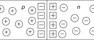
Electric P.'s conductivity can be caused both by the electrons of the own atoms of a given substance (intrinsic conductivity) and by the electrons and holes of impurity atoms (impurity conductivity). The process of introducing impurities into P. to obtain the necessary physical properties. properties is called doping of semiconductors. Since the binding energy of charge carriers in impurity atoms ranges from several meV to several tens of meV, it is impurity conductivity that explains the exponential increase in the concentration of free charge carriers in most atoms in the temperature range near room temperature.
Impurities are usually introduced into polymers during the growth of the structure; they can be donors or acceptors, that is, suppliers of electrons or holes. If, for example, impurity atoms of group V elements (As, P) are introduced into germanium Ge or silicon Si (elements of group IV), then the 4 outer electrons of these atoms form a stable bond with four neighboring atoms of the lattice, and the fifth electron will be unbound and will be held near the impurity atom only due to the Coulomb interaction, weakened by the dielectric. polarization of the environment. Such an impurity atom is a donor and is easily ionized at room temperature. An acceptor appears, for example, when Group III elements (Ga, Al) are introduced into Ge or Si. In this case, to form all four bonds with the nearest atoms, an addition is required. electron, which is taken from the internal shells of atoms, so that the impurity atom is negatively charged. Electroneutrality is restored due to the fact that internal the unfilled orbital is distributed near neighboring atoms of the lattice, located from the impurity at distances exceeding the interatomic distance. The presence of donors or acceptors leads to n- or p-type conductivity, respectively.
Particles in which acceptor and donor impurities can simultaneously exist are called compensated. Compensation for impurities leads to the fact that part of the electrons from donors goes to acceptors, and as a result, the result appears. concentration of ions that effectively influence the conductivity of semiconductors.
The amplitude of the wave function of electrons or holes localized on impurity atoms is 1–10 nm. This means that at a concentration of impurity atoms of approx. 1018 cm–3, the wave functions of electrons and holes of neighboring atoms begin to overlap, charge carriers can move from ion to ion, and the electron becomes degenerate (see Degenerate semiconductors). Such P. are called heavily alloyed. Due to the strong screening of Coulomb attraction, the charge carriers in them are free even at such low temperatures at which thermal interaction was impossible. activation of an electron or hole from an isolated atom.
In the absence of external electrical field or illumination, the concentration of free charge carriers is called equilibrium and is determined by the width of the band gap, the effective masses of charge carriers, the concentration of impurities, and the binding energy of impurity charge carriers.
Along with impurities, sources of charge carriers can also be various. structural defects, e.g. vacancies (the absence of one of the lattice atoms), interstitial atoms, as well as a deficiency or excess of atoms of one of the components in semiconductor compounds (deviations from the stoichiometric composition).
Electron-hole conductivity.
In a “pure” semiconductor crystal, the number of released
at a given moment, electrons are equal to the number of
formed
in this case, therefore the electrical conductivity of such a semiconductor
is small
, since it provides
great
resistance to the electric current, and such electrical conductivity is called
intrinsic
.
But if you add it to a semiconductor as an impurity
a certain number of atoms of other elements, then its electrical conductivity will increase several times, and depending on
the structure
of the atoms of impurity elements, the electrical conductivity of the semiconductor will be
electronic
or
hole
.
Electronic conductivity.
Let's say that in a semiconductor crystal in which the atoms have four valence electrons, we replace one atom with an atom that has five
valence electrons.
This atom with its four
electrons will bond with four neighboring atoms of the semiconductor, and
the fifth
valence electron will remain “
extra
” - that is, free.
And the more
such atoms there are in the crystal, the
more
free electrons there will be, which means that such a semiconductor in its properties will approach the metal, and in order for an electric current to pass through it,
interatomic bonds in it do not necessarily have to be destroyed
.
n” type semiconductors
", or
n
-type semiconductors.
Here the Latin letter n comes from the word “negative” - that is, “negative”. It follows that in an n
-type
the main
charge carriers are
electrons
, and not the main ones are holes.
Hole conductivity.
Let's take the same crystal, but now replace its atom with an atom in which there are only three
free electron.
With its three electrons it will connect only with three
neighboring atoms, and it will not have enough
one
electron to bond with the fourth atom.
As a result, a hole
.
Naturally, it will be filled with any other free electron located nearby, but, in any case, in the crystal of such a semiconductor there will not be enough
electrons to fill the holes.
And the more
such atoms there are in the crystal, the
more
holes there will be.
In order for free electrons to be released and move in such a semiconductor, valence bonds between atoms must be destroyed
.
But there will still not be enough electrons, since the number of holes will always be greater than
the number of electrons at any given time.
hole semiconductors.
conductivity or
p
-type conductors, which translated from the Latin “positive” means “positive”.
Thus, the phenomenon of electric current in a p-type semiconductor crystal is accompanied by the continuous appearance
and
disappearance
of positive charges - holes.
This means that in a p
-type
the main
charge carriers are
holes
, and not the main charge carriers are electrons.
Now that you have some idea of the phenomena occurring in semiconductors, it will not be difficult for you to understand the principle of operation of semiconductor radio components.
Let's stop here, and in the next part we will look at the device, the principle of operation of the diode, we will analyze its current-voltage characteristic and switching circuits. Good luck!
1
.
Borisov V.G. — Young radio amateur. 1985 2
.
Website academic.ru: https://dic.academic.ru/dic.nsf/es/45172.
Electric current in semiconductors. Intrinsic and impurity conductivity
There is a wide class of substances whose specific conductivity occupies an intermediate position between conductors and dielectrics. These substances are usually called semiconductors.
Semiconductors include the twelve chemical elements in the middle part of the periodic table, many metal oxides and sulfides, as well as other chemical compounds.
Let's study the basic properties of conductors using two simple experiments. To do this, we will assemble an electrical circuit consisting of a current source, a switch, a pure semiconductor and a milliammeter. Let's close the circuit. The ammeter shows us that a fairly weak current flows through the circuit. Now let’s heat the semiconductor under study.
It is easy to see how, as its temperature increases, the current in the circuit increases. This indicates that the resistivity of semiconductors does not increase with increasing temperature, like that of metals, but, on the contrary, decreases quite sharply.
In this case, the dependence of semiconductor resistance on temperature is nonlinear. As the temperature decreases, the resistance of semiconductors increases and near absolute zero it becomes as large as that of dielectrics.
Let's return our semiconductor to its original state, but now we will not heat it, but illuminate it using a regular flashlight. By changing the illumination of the semiconductor surface, we observe a change in the milliammeter readings. The results of our observations mean that when the surface of a semiconductor is illuminated, its resistance decreases.
It has been experimentally established that when an electric current passes in pure semiconductors, as in metals, no chemical changes occur, that is, charge transfer during the passage of current is not accompanied by the transfer of matter.
Let's look at the mechanism of conductivity of pure semiconductors using the example of a germanium crystal, the valence of the atoms of which is equal to four. This valency tells us that germanium atoms on the outer shell have four valence electrons relatively weakly associated with the nucleus. In this case, each atom of the crystal is connected to four neighboring atoms through a pair-electronic - covalent bond
. That is, two neighboring atoms combine their two valence electrons (one from each atom), which form an electron pair. Therefore, all valence electrons of the germanium atom participate in the formation of covalent bonds.
At temperatures close to absolute zero, the covalent bonds of germanium are strong enough, so there are no free electrons, and germanium is an insulator.
In order to break a covalent bond and make an electron free, some energy must be imparted to the germanium crystal, for example, by heating the crystal. In this case, some of the electrons receive energy sufficient to leave the atoms and become free, like electrons in metals. In an electric field, they move between lattice nodes, creating an electric current.
The conductivity of semiconductors, due to the presence of free electrons, is called electronic conductivity.
The neutral atom to which the released electron belonged becomes a positively charged ion, and a vacant place with the missing electron is formed in covalent bonds. It's called a hole.
Simultaneously with the process of the formation of free electrons and holes, a process occurs in which one of the electrons (not free, but providing a covalent bond) jumps to the place of the formed hole and restores the covalent bond. In this case, the position of the hole changes, which can be modeled as its movement. Thus, in the absence of an external electric field, a random movement of free electrons and holes is observed in a semiconductor crystal, the concentrations of which are the same in a pure semiconductor.
Holes are considered mobile carriers of a positive charge, which is equal to the modulus of the electron charge. Conductivity due to the movement of holes is called hole conductivity of semiconductors.
Of course, in reality there are no holes as positive charges that actually exist. Nevertheless, the idea of them is a good physical model, which makes it possible to consider the electric current in semiconductors based on the laws of physics.
In the presence of an external electric field, the chaotic movement of free electrons and holes is superimposed on their ordered movement, that is, an electric current arises. Moreover, the movement of free electrons occurs in the direction opposite to the direction of the external electric field strength, and the movement of holes coincides with the direction of the field strength
The conductivity caused by the movement of free electrons and holes in a pure semiconductor is called the intrinsic conductivity of the semiconductor.
But the properties of semiconductors can be changed not only by heating or exposure to electromagnetic radiation, but also by adding impurities to a pure semiconductor.
The conductivity caused by the presence of impurities in the semiconductor is called impurity conductivity of the semiconductor.
Let us consider the mechanism of this conductivity using the example of a germanium crystal containing an admixture of arsenic atoms, the valency of which is five.
So, the four valence electrons of the arsenic atom form covalent bonds with neighboring germanium atoms. The fifth electrons of arsenic atoms are not involved in the formation of covalent bonds and can move freely, much like electrons in a metal conductor. The conductivity of such a crystal will be predominantly electronic. Such semiconductors are called electronic semiconductors or
n
-type
(from the Latin negative).
Impurities that supply free electrons to semiconductors without creating an equal number of holes are called donor impurities.
(that is, giving). The resistivity of a semiconductor containing such impurities decreases sharply and can approach the resistivity of a metal conductor.
Now let's replace the arsenic atoms with trivalent indium atoms. It is obvious that the valence electrons of the indium atom form covalent bonds with only three neighboring germanium atoms. The indium atom does not have an electron to form a bond with the fourth germanium atom. Therefore, near each indium atom one of the covalent bonds will be unfilled, that is, a hole appears. This missing electron can be captured by the indium atom from the covalent bond of neighboring germanium atoms. But in this case, a hole is formed in the place where the electron was previously located.
As a result of the introduction of such an impurity, many covalent bonds in the crystal are broken and holes are formed. The conductivity of such a crystal will be predominantly hole
.
Such semiconductors are called hole semiconductors.
or
p
-type semiconductors (from the Latin positive).
Impurities, the presence of which in a semiconductor leads to the formation of holes without increasing the number of free electrons, are called acceptor impurities.
(i.e. receiving). The resistivity of semiconductors containing acceptor impurities also decreases sharply.
The most interesting phenomena occur when semiconductors come into contact with
- and
p
-types. These phenomena are used in most semiconductor devices.
The contact of two conductors with different types of conductivity is called an electron-hole junction or, abbreviated as p-p
-transition.
Free electron concentration in n
-region is significantly higher than in
the p
-region; accordingly, the concentration of holes, that is, vacancies in
the p
-region is significantly greater than their concentration in
the n
-region.
As soon as the semiconductors are brought into contact, electrons begin to diffuse from the region with conductivity n
p
conductivity and, accordingly, the transition of holes in the opposite direction.
the p
semiconductor occupy free spaces, the process of recombination of electrons and holes occurs, and the holes that have entered the
n
-type semiconductor also disappear due to the electrons occupying the vacant space.
As a result of diffusion, a double electrical layer of oppositely charged ions is formed at the boundary between these regions, the thickness of which does not exceed fractions of a micrometer. An electric field arises between the layers of ions, which prevents the further transition of the main charge carriers across the interface. In other words, in the transition zone between semiconductors of different types, a so-called blocking layer
.
Let's assemble an electrical circuit consisting of a current source, a light bulb and a semiconductor with n
-
p
-transition.
In this case, we connect the positive pole of the current source to the p
-region, and the negative pole to
the n
-region. When the circuit is closed, the light will glow. The conclusion is obvious: electric current passes through the circuit.
This phenomenon can be explained as follows. Under the influence of the electric field created by the current source, the blocking layer begins to disappear, since the strength of the external electric field of the source is opposite in the direction of the field strength of the blocking layer and almost completely compensates for it. This leads to the resumption of diffusion of the majority charge carriers through n
-
p
-transition.
In this case, the n
-
p
junction is switched on in
the forward direction or, they say, in the through direction.
Now let’s change the connection of the semiconductor to the current source.
When the circuit is closed, the light does not light, that is, there is no current in the circuit. The reason is that the thickness of the blocking layer and, therefore, its resistance increases, since the direction of the electric field strength created by the source coincides with the direction of the field strength of the blocking layer.
In this case n
—
the p
-junction is switched on in
the reverse (blocking) direction
and there is practically no current through the junction (if you do not take into account the current created by minority carriers, the concentration of which is small compared to the concentration of the majority current carriers).
Thus, the n-p junction in a semiconductor has one-way conductivity.
This property of semiconductors is widely used in devices called semiconductor
diodes
. They are the main components of AC rectifiers and electromagnetic signal detectors.
Valence of atoms
Atoms that have 6 or 7 electrons in their outer orbit tend to attach 1 or 2 electrons to themselves. Such atoms are said to be monovalent or divalent. But if there are 1, 2 or 3 electrons in the outer orbit of an atom, then such an atom tends to give them away. In this case, the atom is considered to be one, two or three valent.
If the outer orbit of an atom contains 4 electrons, then such an atom prefers to unite with the same one, which also has 4 electrons. This is how germanium and silicon atoms are combined to make transistors. In this case, the atoms are called tetravalent. (Germanium or silicon atoms can also combine with other elements, such as oxygen or hydrogen, but these compounds are not interesting for our story.)
Germanium (silicon) atom (Fig. 3)
In Fig. Figure 3 shows an atom of germanium or silicon wanting to combine with a similar atom. The small black circles are the atom's own electrons, and the light circles indicate the places where the electrons of the four neighboring atoms will fall.
Semiconductor crystal lattice
To understand the features of semiconductors, consider the crystal lattice of a typical semiconductor - germanium or silicon.
Rice. 2. Crystal lattice of a semiconductor.
The bond between atoms in a semiconductor crystal is covalent. That is, the electron orbits of neighboring atoms overlap, and the electrons become common so that the total number of electrons in the shell of each atom comes to an energetically stable number - 8 electrons.
Silicon is tetravalent, it has four electrons in its electron shell, and it has four neighbors in the crystal lattice. As a result, it is “energetically favorable” for silicon to form four two-electron covalent bonds with neighboring atoms. The electron shell of each atom will have 8 electrons - four of its own, and one from each of its neighbors. The electrons turn out to be “common to the entire crystal.” Having approached one atom in orbit, they can continue to move along the orbit of another atom, then a third, and so on.
Physical properties and applications
First of all, it should be said that the physical properties of semiconductors are the most studied in comparison with metals and dielectrics. To a large extent, this is facilitated by a huge number of effects that cannot be observed in either one or another substance, primarily related to the structure of the band structure of semiconductors and the presence of a fairly narrow band gap. Of course, the main incentive for studying semiconductors is the production of semiconductor devices and integrated circuits - this primarily applies to silicon, but also affects other compounds (Ge, GaAs, InP, InSb).
Silicon is an indirect-gap semiconductor, the optical properties of which are widely used to create photodiodes and solar cells, but it is very difficult to make it work as a light source, and here there is no competition from direct-gap semiconductors - compounds of the III-V type, among which are GaAs, GaN, which are used for creation of LEDs and semiconductor lasers.
An intrinsic semiconductor at absolute zero temperature does not have free carriers in the conduction band, unlike conductors, and behaves like a dielectric. When doping, the situation may change (see degenerate semiconductors).
Due to the fact that technologists can obtain very pure substances, the question arises about a new standard for Avogadro's number.
Alloying
The bulk properties of a semiconductor can greatly depend on the presence of defects in the crystal structure. And therefore they strive to grow very pure substances, mainly for the electronics industry. Dopants are introduced to control the amount and type of conductivity of the semiconductor. For example, widespread silicon can be doped with an element of the V subgroup of the periodic table of elements - phosphorus, which is a donor, and create n-Si. To obtain silicon with hole type conductivity (p-Si), boron (acceptor) is used. Compensated semiconductors are also created in order to fix the Fermi level in the middle of the bandgap.
p type semiconductors
In a semiconductor that contains an acceptor impurity, electrons move quite easily from the valence band to acceptor levels. In such a situation, free holes appear in the valence band. The number of holes in this case is significantly greater than the number of free electrons that were formed during the transition from the valence band to the conduction band. In this situation, holes are the majority charge carriers, electrons are minority carriers. The conductivity of a semiconductor that includes an acceptor impurity is of a hole nature; the conductor itself is called a hole (acceptor) or p-type semiconductor (positive). The energy diagram of a p-type semiconductor is shown in Fig. 2.
Picture 1.
Finished works on a similar topic
Course work Semiconductors of p and n type, pn junction 400 ₽ Abstract Semiconductors of p and n type, pn junction 250 ₽ Test work Semiconductors of p and n type, pn junction 190 ₽
Receive completed work or specialist advice on your educational project Find out the cost
Figure 2.
p - n Transition .
A pn junction is the simplest semiconductor structure that is used in most semiconductor devices. To obtain a pn junction, a semiconductor sample is doped (impurities are introduced into it) in such a way that donor impurities predominate in one part and acceptor impurities in the other, resulting in contact between an n-type semiconductor and a p-type semiconductor.
The main property of a pn junction is its ability to pass current in only one direction if a voltage is applied to the sample so that the conduction is carried out by the main current carriers, as shown in the figure above: “-” on the side of the n-type semiconductor, “+” - from the p-type side (electrons from the n-region move to the p-region, and vice versa).
If we now change the polarity of the applied voltage U, then practically no current flows through the pn junction, since the transition through the contact is carried out by minority carriers, of which there are few. The current-voltage characteristic of the p-n junction is shown in the figure below.
Type n semiconductors
The introduction of impurities into a semiconductor significantly affects the behavior of electrons and the energy levels of the crystal spectrum.
The valence electrons of impurity atoms create energy levels in the band gap of the spectrum. For example, if in the germanium lattice one atom is replaced by a pentavalent fluorine atom, then the energy of the additional electron will become less than the energy that corresponds to the lower boundary of the conduction band. The energy levels of such impurity electrons are below the bottom of the conduction band. These levels filled with electrons are called donor levels. To transfer electrons from donor levels to the conduction band, the energy required is less than that of a pure semiconductor. After electrons are transferred to the conduction band from donor levels, they say that n-type conductivity has appeared in the semiconductor. Semiconductors with a donor impurity are called electronic (donor) or n-type (negative) semiconductors. Electrons in n-type semiconductors serve as the majority charge carriers, while holes serve as minority charge carriers. The energy diagram of such a semiconductor is shown in Fig. 1. Are you an expert in this subject area? We invite you to become the author of the Directory Working Conditions
Symmetrical current-voltage characteristic
When the polarity of the voltage changes, the current in the semiconductor begins to flow in the opposite direction. And it changes according to the same law. This suggests that the semiconductor element has a symmetrical current-voltage characteristic. If one part of the element is of the hole type, and the second is of the electronic type, then a pn junction (electron-hole) appears at the boundary of their contact. It is precisely these transitions that are present in all elements - transistors, diodes, microcircuits. But only in microcircuits several transistors are assembled on one chip at once - sometimes there are more than a dozen of them.
Semiconductor optics
The absorption of light by semiconductors is due to transitions between energy states of the band structure. Given the Pauli exclusion principle, electrons can only move from a filled energy level to an unfilled one. In an intrinsic semiconductor, all states of the valence band are filled, and all states of the conduction band are unfilled, so transitions are possible only from the valence band to the conduction band. To make such a transition, the electron must receive energy from light that exceeds the band gap. Photons with lower energy do not cause transitions between the electronic states of the semiconductor, therefore such semiconductors are transparent in the frequency range ωEgℏ{\displaystyle \omega , where Eg{\displaystyle E_{g}} is the band gap, ℏ{\displaystyle \hbar } is a constant Plank. This frequency determines the fundamental absorption edge for the semiconductor. For semiconductors, which are often used in electronics (silicon, germanium, gallium arsenide), it lies in the infrared region of the spectrum.
Additional restrictions on the absorption of light by semiconductors are imposed by selection rules, in particular the law of conservation of momentum. The law of conservation of momentum requires that the quasi-momentum of the final state differ from the quasi-momentum of the initial state by the magnitude of the momentum of the absorbed photon. The wave number of a photon is 2πλ{\displaystyle 2\pi /\lambda }, where λ{\displaystyle \lambda } is the wavelength, is very small compared to the wave vector of the reciprocal lattice of the semiconductor, or, which is the same, the wavelength of the photon in the visible regions are much larger than the characteristic interatomic distance in a semiconductor, which leads to the requirement that the quasimomentum of the final state during an electronic transition be practically equal to the quasi-momentum of the initial state. At frequencies close to the fundamental absorption edge, this is only possible for direct-gap semiconductors. Optical transitions in semiconductors, in which the electron momentum remains almost unchanged, are called direct transitions
or
vertical
.
The momentum of the final state can differ significantly from the momentum of the initial state if another, third particle, for example, a phonon, is involved in the process of photon absorption. Such transitions are also possible, although less likely. These are called indirect transitions
.
Thus, direct-gap semiconductors such as gallium arsenide begin to strongly absorb light when the quantum energy exceeds the bandgap. Such semiconductors are very convenient for use in optoelectronics.
Indirect bandgap semiconductors, for example, silicon, absorb light in the frequency range of light with a quantum energy slightly greater than the bandgap width much weaker, only due to indirect transitions, the intensity of which depends on the presence of phonons, and therefore on temperature. The cutoff frequency of direct transitions in silicon is greater than 3 eV, that is, it lies in the ultraviolet region of the spectrum.
When an electron passes from the valence band to the conduction band, free charge carriers appear in the semiconductor, and hence photoconductivity.
At frequencies below the fundamental absorption edge, absorption of light is also possible, which is associated with excitation of excitons, electronic transitions between impurity levels and allowed bands, as well as absorption of light by lattice vibrations and free carriers. Exciton bands are located in the semiconductor slightly below the bottom of the conduction band due to the exciton binding energy. Exciton absorption spectra have a hydrogen-like structure of energy levels. Similarly, impurities, acceptors or donors, create acceptor or donor levels lying in the band gap. They significantly modify the absorption spectrum of the doped semiconductor. If during an indirect gap transition a phonon is absorbed simultaneously with a light quantum, then the energy of the absorbed light quantum may be less by the amount of the phonon energy, which leads to absorption at frequencies slightly lower in energy from the fundamental absorption edge.
Self conductivity
If you connect a semiconductor element to an electrical circuit and start heating it, the current in the circuit increases. Consequently, the resistance of the semiconductor decreases
with increasing temperature. Why is this happening?
As the temperature rises, the thermal vibrations of silicon atoms become more intense, and the energy of the valence electrons increases. For some electrons, the energy reaches values sufficient to break covalent bonds. Such electrons leave their atoms and become free
(or
conduction electrons
) - exactly the same as in a metal. In an external electric field, free electrons begin to move in an orderly manner, forming an electric current.
The higher the silicon temperature, the greater the electron energy, and the greater the number of covalent bonds that fail and break. The number of free electrons in a silicon crystal increases, which leads to a decrease in its resistance.
The breaking of covalent bonds and the appearance of free electrons is shown in Fig. 5. A hole
— vacant place for an electron.
The hole has a positive
charge, since with the departure of a negatively charged electron, an uncompensated positive charge of the nucleus of the silicon atom remains.
Rice. 5. Formation of free electrons and holes
The holes do not stay in place - they can wander around the crystal. The fact is that one of the neighboring valence electrons, “traveling” between atoms, can jump to the resulting vacant place, filling the hole; then the hole in this place will disappear, but will appear in the place where the electron came from.
In the absence of an external electric field, the movement of holes is random, because valence electrons wander randomly between atoms. However, in an electric field a directional direction
movement of holes. Why? This is not difficult to understand.
In Fig. Figure 6 shows a semiconductor placed in an electric field. On the left side of the picture is the initial position of the hole.
Rice. 6. Motion of a hole in an electric field
Where will the hole go? It is clear that the most likely electron > hole jumps are in the opposite
field lines (that is, to the “pluses” that create the field). One of these jumps is shown in the middle part of the figure: the electron jumped to the left, filling the vacancy, and the hole, accordingly, shifted to the right. The next possible electron jump caused by the electric field is depicted on the right side of the figure; As a result of this jump, the hole took a new place, located even further to the right.
We see that the hole as a whole moves in the direction
field lines - that is, where positive charges are supposed to move. Let us emphasize once again that the directed movement of a hole along the field is caused by jumps of valence electrons from atom to atom, occurring predominantly in the direction against the field.
Thus, in a silicon crystal there are two types of charge carriers: free electrons and holes. When an external electric field is applied, an electric current appears, caused by their ordered counter motion: free electrons move opposite to the field strength vector, and holes move in the direction of the vector.
The generation of current due to the movement of free electrons is called electronic conductivity
, or
n-type conductivity
.
The process of ordered movement of holes is called hole conductivity
, or
p-type conductivity
(from the first letters of the Latin words negativus (negative) and positivus (positive)).
Both electron and hole conductivities are collectively called the intrinsic conductivity
of a semiconductor.
Each electron leaving a broken covalent bond generates a “free electron–hole” pair. Therefore, the concentration of free electrons in a pure silicon crystal is equal to the concentration of holes. Accordingly, when the crystal is heated, the concentration of not only free electrons, but also holes increases, which leads to an increase in the intrinsic conductivity of the semiconductor due to an increase in both electron and hole conductivity.
Along with the formation of free electron–hole pairs, the reverse process also occurs: recombination
free electrons and holes.
Namely, a free electron, encountering a hole, fills this vacancy, restoring the broken covalent bond and turning into a valence electron. Thus, a dynamic equilibrium
: the average number of breaks of covalent bonds and the formation of electron-hole pairs per unit time is equal to the average number of recombining electrons and holes. This state of dynamic equilibrium determines the equilibrium concentration of free electrons and holes in the semiconductor under given conditions.
Changes in external conditions shift the state of dynamic equilibrium in one direction or another. In this case, the equilibrium value of the charge carrier concentration naturally changes. For example, the number of free electrons and holes increases when the semiconductor is heated or illuminated.
At room temperature, the concentration of free electrons and holes in silicon is approximately equal to cm. The concentration of silicon atoms is on the order of cm. In other words, there is only one free electron per silicon atom! This is very little. In metals, for example, the concentration of free electrons is approximately equal to the concentration of atoms. Accordingly, the intrinsic conductivity of silicon and other semiconductors under normal conditions is small compared to the conductivity of metals
.
Types of semiconductors, oxides
Metal oxides are generally excellent insulators, but there are exceptions. Examples of this type of semiconductors are nickel oxide, copper oxide, cobalt oxide, copper dioxide, iron oxide, europium oxide, zinc oxide. Since copper dioxide exists in the form of the mineral cuprite, its properties have been extensively studied. The procedure for growing this type of semiconductor is not yet fully understood, so their use is still limited. An exception is zinc oxide (ZnO), a compound of groups 2-6, used as a converter and in the production of adhesive tapes and adhesives.
The situation changed dramatically after superconductivity was discovered in many compounds of copper with oxygen. The first high-temperature superconductor discovered by Müller and Bednorz was a compound based on the semiconductor La2CuO4 with an energy gap of 2 eV. By replacing trivalent lanthanum with divalent barium or strontium, hole charge carriers are introduced into the semiconductor. Achieving the required hole concentration turns La2CuO4 into a superconductor. At this time, the highest temperature of transition to the superconducting state belongs to the compound HgBaCa2Cu3O8. At high pressure its value is 134 K.
ZnO, zinc oxide, is used in varistors, blue LEDs, gas sensors, biological sensors, window coatings to reflect infrared light, as a conductor in LCD displays and solar cells. dE=3.37 eV.
How molecules are made from atoms
Any atom is in a stable state if there are 8 electrons in its outer orbit. It does not seek to take electrons from neighboring atoms, but it does not give up its own. To verify the validity of this, it is enough to look at the inert gases in the periodic table: neon, argon, krypton, xenon. Each of them has 8 electrons in the outer orbit, which explains the reluctance of these gases to enter into any relationships (chemical reactions) with other atoms or to build molecules of chemical substances.
The situation is completely different for those atoms that do not have the coveted 8 electrons in their outer orbit. Such atoms prefer to unite with others in order to supplement their outer orbit with up to 8 electrons and achieve a calm, stable state.
For example, here is the well-known water molecule H2O. It consists of two hydrogen atoms and one oxygen atom, as shown in Fig. 1.
How a water molecule is created (Fig. 1)
At the top of the figure, two hydrogen atoms and one oxygen atom are shown separately. There are 6 electrons in the outer orbit of oxygen and two electrons in two hydrogen atoms nearby. Oxygen lacks just two electrons in its outer orbit to reach the coveted number 8, which it will receive by attaching two hydrogen atoms to itself.
Each hydrogen atom lacks 7 electrons in its outer orbit to be completely happy. The first hydrogen atom receives 6 electrons from oxygen into its outer orbit and one more electron from its twin, the second hydrogen atom. There are now 8 electrons in its outer orbit along with its electron. The second hydrogen atom also completes its outer orbit to the coveted number 8. This process is shown in the lower part of Fig. 1.
In Fig. Figure 2 shows the process of combining sodium and chlorine atoms. The result is sodium chloride, which is sold in stores under the name table salt.
The process of combining sodium and chlorine atoms (Fig. 2)
Here, too, each of the participants receives from the other the missing number of electrons: chlorine adds a single sodium electron to its own seven electrons, while it gives its own to the sodium atom. Both atoms have 8 electrons in the outer orbit, which ensures complete agreement and well-being.
Self-density
At thermodynamic equilibrium, the electron concentration of a semiconductor is related to temperature by the following relationship:
n¯=2h3(2πmkT)32e−EC−EFkT{\displaystyle {\bar {n}}={\frac {2}{h^{3}}}(2\pi mkT)^{3/2}e ^{-{\frac {E_{C}-E_{F}}{kT}}}}
Where:
h{\displaystyle h} — Planck's constant; m{\displaystyle m}—electron mass; T{\displaystyle T} - absolute temperature; EC{\displaystyle E_{C}} — conduction band level; EF{\displaystyle E_{F}} is the Fermi level.
Also, the hole concentration of a semiconductor is related to temperature by the following relationship:
p¯=2h3(2πmkT)32e−EF−EVkT{\displaystyle {\bar {p}}={\frac {2}{h^{3}}}(2\pi mkT)^{3/2}e ^{-{\frac {E_{F}-E_{V}}{kT}}}}
Where:
h{\displaystyle h} — Planck's constant. m{\displaystyle m} is the effective mass of the hole; T{\displaystyle T} - absolute temperature; EF{\displaystyle E_{F}}—Fermi level; EV{\displaystyle E_{V}} is the valence band level.
The intrinsic concentration ni{\displaystyle n_{i}} is related to n¯{\displaystyle {\bar {n}}} and p¯{\displaystyle {\bar {p}}} by the following relation:
n¯p¯=ni2{\displaystyle {\bar {n}}{\bar {p}}=n_{i}^{2}}
Semiconductor devices
We can immediately give examples of semiconductor devices - these are transistors, thyristors, diodes, and even microcircuits. Of course, this is not a complete list. To make a semiconductor device, you need to use materials that have hole or electron conductivity. To obtain such a material, it is necessary to introduce an additive into an ideally pure semiconductor with an impurity concentration of less than 10-11% (it is called a dopant).
Those impurities whose valency is greater than that of the semiconductor give up free electrons. These impurities are called donors. But those whose valence is less than that of a semiconductor tend to grab and hold electrons. They are called acceptors. In order to obtain a semiconductor that will have only electronic-type conductivity, it is enough to introduce into the source material a substance whose valence will be only one more. For an example of semiconductors, in the physics course of the school course, germanium is considered - its valence is 4. A donor is added to it - phosphorus or antimony, their valence is equal to five. There are few semiconductor metals; they are practically not used in technology.
In this case, 4 electrons in each atom establish four paired (covalent) bonds with germanium. The fifth electron does not have such a bond, which means it is in a free state. And if you apply voltage to it, it will form an electronic current.
Methods for determining the type of electrical conductivity and parameters of semiconductors
Type of semiconductor electrical conductivity ( n
or
p
) can be determined experimentally using the Hall effect. The American physicist Hall in 1879 discovered an interesting and practically important phenomenon - the occurrence of transverse EMF in a conductor with a current placed in a magnetic field. After the name of the scientist who discovered this phenomenon, the transverse emf arising in a magnetic field is called Hall emf or Hall voltage. The physical essence of the Hall effect is complex and below is only a simplified representation of this phenomenon.
The essence of the method for determining the type of electrical conductivity of the semiconductor under test is based on the change in the sign of the transverse Hall EMF depending on the type of charge carriers. The experimental diagram is shown in Fig. 2.9 .
A semiconductor wafer is placed in an external transverse magnetic field, with induction B
.
A potential difference is applied along the length of the semiconductor, creating electric field strength E.
Under the influence of this field, an electric current arises in the semiconductor, i.e.
directional movement of electric charges occurs. The magnetic field acts on moving charges with some force. This force moves moving charge carriers to one of the faces of the semiconductor wafer. As a result, a transverse EMF arises, which is measured with a voltmeter V.
The direction of charge displacement is determined by the “left hand” rule, which relates to the technical direction of the current. The positive direction of current is the direction of movement of positive charges, i.e. direction opposite to the direction of electron drift. From Fig. 2.9 it is clear that when the type of electrical conductivity changes, the polarity of the voltage on the voltmeter also changes.
For semiconductors with one type of charge carrier ( n
or
p
) equality (2.9) takes the form:
or (4.14)
Charge carrier concentration ( n0
and
p0
) and their mobility (
un
and
up
) are
characteristic parameters
of the semiconductor. By measuring the conductivity of a semiconductor, it is possible, in accordance with formula (2.14), to determine only the product of these two parameters. To determine each of them, you can use the Hall effect, which consists in the displacement of moving charge carriers under the influence of the Lorentz force to one of the faces of the semiconductor.
The displacement of charge carriers in the transverse direction in the semiconductor will stop when the Lorentz force is balanced by the Coulomb force acting on the charges from the emerging transverse electric field of the displaced charges. Moreover, in the semiconductor under study (for example, n
-type) the following relations will be satisfied:
(4.15)
Here: - the force acting from the electric field on an electron having a charge e
=1.6∙10-19 C;
B
– magnetic induction created by an external source of magnetic field, and having a direction perpendicular to the direction of the current density vector in the semiconductor;
I
– direct current passing through the conductor;
n0
– concentration of charge carriers;
e
– electron charge;
is the average drift velocity of charge carriers under the influence of an external electric field E;
h, x —height and width of the semiconductor;
S
=
hx
is the cross section of the semiconductor through which current
I passes;
— Hall voltage.
Using relations (2.15), we express the Hall voltage in scalar form:
, (2.16)
here is the Hall coefficient, which has the dimension m3/C in the SI system.
Fig.4.9. Experimental determination of the type of electrical conductivity of a semiconductor using the Hall effect.
Task 2.2 . Rectangular n-type semiconductor sample (Fig. 2.9) with dimensions x
=5mm,
h
=2mm and length
l
=50mm, placed in a magnetic field with induction
B
=0.5T.
The magnetic induction vector is perpendicular to the sample plane. Ua
is applied along the semiconductor , under the influence of which a current
Ia
= 40 mA flows.
The voltmeter V shows the Hall voltage Ux
=6.2mV. Find the conductivity, mobility, and carrier concentration for this semiconductor, assuming that conductivity is due only to electrons.
Solution
. Semiconductor resistance:
Ohm.
Semiconductor resistivity:
Ohm m.
Conductivity:
cm m-1.
In accordance with formula (2.15), we determine the Hall coefficient:
m3/Cl.
From the relationship we determine the electron concentration:
m-3.
From expression (2.8) we determine the electron mobility:
m2/(V s).
Transverse emf or transverse Hall voltage, current I
, magnetic induction
B
and the thickness of the semiconductor wafer
h
can be measured, which allows using formula (2.16) to calculate the value of the Hall coefficient X. The value of the coefficient obtained from formula (2.16) is valid only for
degenerate
semiconductors, i.e. for semiconductors with very a high impurity concentration, at which its activation energy is close to zero and the velocity distribution of charge carriers can be ignored.
Equations (2.15) were written with these assumptions. A more accurate value of the Hall coefficient for semiconductors with different impurity concentrations will differ from that obtained from formula (2.16) by the factor A.
For semiconductors of various groups, the numerical value of the coefficient
A
varies from one to two depending on the mechanism of carrier scattering at different temperatures (for example, for germanium
A
» 1.18).
Thus, for n-
type
. (4.17)
For hole semiconductors, it is easy to obtain a similar expression that differs in sign and includes the carrier concentration p.
Using equations (4.17) and (4.14), one can find the numerical values of the concentration and mobility of charge carriers in semiconductors.
Thus, knowing the direction of the Hall emf, we can determine the sign of the charge carriers ( n
or
p-
electrical conductivity), and using formula (4.17) to determine the concentration of charge carriers.
The above formulas applied to semiconductors of pronounced p-
or
p-
type, in which the concentration of minority carriers is negligible compared to the concentration of majority carriers. If the concentration of minority carriers is such that they begin to significantly influence the movement of majority carriers in a semiconductor located in a magnetic field, then when calculating the Hall coefficient it is necessary to take into account both types of carriers. The calculation in this case is more complicated.
The Hall effect is interesting not only as the basis for a method for determining the characteristics of semiconductor materials, but also as the operating principle of some semiconductor devices, which are used, for example, to measure magnetic field strength, multiply two quantities, and other purposes.
Note that the displacement of charge carriers in a semiconductor under the influence of a magnetic field to one of the faces, along with the appearance of a Hall voltage, also creates an increase in the resistance of the semiconductor, since its effective cross section decreases.
The type of electrical conductivity of a semiconductor can also be determined by heating one end of the test semiconductor using the Seebeck phenomenon, as shown in Fig. 4.10.
When testing an
n-
type semiconductor, a greater number of electrons will be released at the hot end due to the expenditure of external thermal energy than at the cold end. As a result, the concentration of free charge carriers (electrons) at the hot end of the semiconductor will be greater than at the cold end, and their diffusion will begin from the hot to the cold end, where the concentration of free carriers is lower. Due to the loss of electrons, the hot end becomes positively charged and the cold end negatively charged. A potential difference arises between the ends of the semiconductor. Under the influence of this potential difference, an electric field arises inside the semiconductor, which causes a counter flow of electrons from the cold end to the hot one. A stationary state is established when these electron flows are equal.
If a semiconductor p-
type, then at the heated end, due to the expenditure of thermal energy, a larger number of electrons will be transferred from the filled zone to the acceptor levels of impurities compared to the cold end.
There is an excess concentration of holes at the hot end. Holes will begin to diffuse from the hot end to the cold end, and it will become negatively charged relative to the cold end.
and therefore the type of electrical conductivity, is determined using a voltmeter V.
Fig.4.10. Experimental determination of the type of electrical conductivity of a semiconductor by heating one of its ends.
The opposite effect to the Seebeck phenomenon is called the Thompson effect. The Thompson effect is the release or absorption of heat when a current passes through a homogeneous material in which there is a temperature gradient. The presence of a temperature gradient in a semiconductor leads to the formation of thermoEMF. If the direction of the external electric field coincides with the electric field formed by thermoEMF, then when current passes, the semiconductor cools. If the direction of the external electric field changes to the opposite, then the forces of the electric field during the passage of an electric current will do additional work, as a result of which additional heat is released in relation to the Joule heat.
Note that when current passes through the contact of two dissimilar semiconductors or a semiconductor and a metal, heat is also absorbed or released depending on the direction of the current. The amount of heat released or absorbed in a contact per unit time is proportional to the value of the flowing current. This phenomenon is called the Peltier effect.
LECTURE 5. MAGNETIC MATERIALS, THEIR CLASSIFICATION. PROCESS OF NHAMAGNETIZATION OF FERROMAGNETS. MAGNETIZATION LOSSES, APPLICATION AREA
Magnetic semiconductors
Compounds with magnetic ions of europium and manganese have interesting magnetic and semiconductor properties. Examples of semiconductors of this type are europium sulfide, europium selenide and solid solutions like Cd1-xMnxTe. The content of magnetic ions affects how magnetic properties such as antiferromagnetism and ferromagnetism appear in substances. Semimagnetic semiconductors are solid magnetic solutions of semiconductors that contain magnetic ions in small concentrations
Such solid solutions attract attention due to their promise and great potential for possible applications. For example, unlike non-magnetic semiconductors, they can achieve a million times greater Faraday rotation
The strong magneto-optical effects of magnetic semiconductors allow them to be used for optical modulation. Perovskites like Mn0.7Ca0.3O3 have properties superior to the metal-semiconductor transition, the direct dependence of which on the magnetic field results in the phenomenon of giant magnetoresistance. They are used in radio engineering and optical devices that are controlled by a magnetic field, in waveguides of microwave devices.
Types of semiconductors in the periodic table of elements
The table below provides information on a large number of semiconductor elements and their connections, divided into several types:
- single-element semiconductors of group IV of the periodic table of elements,
- complex: two-element AIIIBV and AIIBVI from the third and fifth groups and from the second and sixth groups of elements, respectively.
All types of semiconductors have an interesting dependence of the band gap on the period, namely, as the period increases, the band gap decreases.
| Group | IIB | IIIA | IVA | V.A. | VIA |
| Period | |||||
| 2 | 5 B | 6 C | 7N | ||
| 3 | 13 Al | 14 Si | 15P | 16 S | |
| 4 | 30 Zn | 31 Ga | 32 Ge | 33 As | 34 Se |
| 5 | 48 Cd | 49 In | 50 Sn | 51 Sb | 52 Te |
| 6 | 80 Hg |
Hole conductivity.
The breaking of valence bonds with increasing temperature leads to the formation of a vacant site with a missing electron, which has an effective positive charge and is called a hole. It becomes possible for valence electrons to move from neighboring bonds to the vacated space. This movement of a negative charge (electron) in one direction is equivalent to the movement of a positive charge (hole) in the opposite direction.
The movement of holes throughout the crystal occurs chaotically, but if a potential difference is applied to it, they will begin to move directionally along the electric field. The conductivity of a crystal due to holes is called hole conductivity.
Electronic and hole conductivity of pure (pure) semiconductors is called intrinsic conductivity of semiconductors.
Impurity conductivity of semiconductors
The conductivity of semiconductors increases with the introduction of impurities, when, along with their own conductivity, additional impurity conductivity appears.
Impurity conductivity
semiconductors is called conductivity due to the presence of impurities in the semiconductor.
Impurity centers can be:
1. atoms or ions of chemical elements embedded in a semiconductor lattice;
2. excess atoms or ions embedded in the interstices of the lattice;
3. various other defects and distortions in the crystal lattice: empty nodes, cracks, shifts that occur during deformation of crystals, etc.
By changing the concentration of impurities, you can significantly increase the number of charge carriers of one sign or another and create semiconductors with a predominant concentration of either negatively or positively charged carriers.
Impurities can be divided into donor (giving away) and acceptor (receiving) impurities.
Donor impurity
- From the Latin “donare” - to give, to sacrifice.
Let us consider the mechanism of electrical conductivity of a semiconductor with a donor pentavalent arsenic impurity As, which is introduced into a crystal, for example, silicon. The pentavalent arsenic atom donates four valence electrons to form covalent bonds, and the fifth electron is unoccupied in these bonds (Fig. 8).
Rice. 8
The abstraction energy (ionization energy) of the fifth valence electron of arsenic in silicon is 0.05 eV = 0.08⋅10-19 J, which is 20 times less than the energy of electron abstraction from a silicon atom. Therefore, already at room temperature, almost all arsenic atoms lose one of their electrons and become positive ions. Positive arsenic ions cannot capture electrons from neighboring atoms, since all four bonds are already equipped with electrons. In this case, there is no movement of the electron vacancy—the “hole”—and the hole conductivity is very small, i.e. practically absent.
Donor impurities
- these are impurities that easily give up electrons and, therefore, increase the number of free electrons. In the presence of an electric field, free electrons come into ordered motion in a semiconductor crystal, and electronic impurity conductivity appears in it. The result is a semiconductor with predominantly electronic conductivity, called an n-type semiconductor. (From Latin negativus - negative).
Since in an n-type semiconductor the number of electrons is much greater than the number of holes, electrons are the majority charge carriers, and holes are minority carriers.
Acceptor impurity
- From the Latin “acceptor” - receiver.
In the case of an acceptor impurity, for example, trivalent indium In, the impurity atom can give its three electrons to carry out a covalent bond with only three neighboring silicon atoms, and one electron is “missing” (Fig. 9). One of the electrons of neighboring silicon atoms can fill this bond, then the In atom will become a stationary negative ion, and a hole will form in the place of the electron that left one of the silicon atoms. Acceptor impurities, capturing electrons and thereby creating mobile holes, do not increase the number of conduction electrons. The majority charge carriers in a semiconductor with an acceptor impurity are holes, and the minority charge carriers are electrons.
Rice. 9
Acceptor impurities
- These are impurities that provide hole conductivity.
Semiconductors in which the concentration of holes exceeds the concentration of conduction electrons are called p-type semiconductors (From the Latin positivus - positive.).
It should be noted that the introduction of impurities into semiconductors, as in any metals, disrupts the structure of the crystal lattice and impedes the movement of electrons. However, the resistance does not increase due to the fact that increasing the concentration of charge carriers significantly reduces the resistance. Thus, the introduction of a boron impurity in an amount of 1 atom per hundred thousand silicon atoms reduces the electrical resistivity of silicon by approximately a thousand times, and an admixture of one indium atom per 108 - 109 germanium atoms reduces the electrical resistivity of germanium by millions of times.
If both donor and acceptor impurities are simultaneously introduced into a semiconductor, then the nature of the semiconductor’s conductivity (n- or p-type) is determined by the impurity with a higher concentration of charge carriers.