1.13. Electric current in semiconductors
In terms of electrical resistivity, semiconductors occupy an intermediate position between good conductors and dielectrics. Semiconductors include many chemical elements (germanium, silicon, selenium, tellurium, arsenic, etc.), a huge number of alloys and chemical compounds. Almost all inorganic substances in the world around us are semiconductors. The most common semiconductor in nature is silicon, which makes up about 30% of the earth's crust.
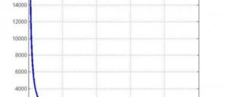
The qualitative difference between semiconductors and metals is manifested primarily in the dependence of resistivity on temperature. As the temperature decreases, the resistance of metals decreases (see Fig. 1.12.4). In semiconductors, on the contrary, the resistance increases with decreasing temperature and near absolute zero they practically become insulators (Fig. 1.13.1).
| Figure 1.13.1. Dependence of resistivity ρ of a pure semiconductor on absolute temperature T |
This behavior of the ρ(T) dependence shows that in semiconductors the concentration of free charge carriers does not remain constant, but increases with increasing temperature. The mechanism of electric current in semiconductors cannot be explained within the framework of the free electron gas model. Let us qualitatively consider this mechanism using the example of germanium (Ge). In a silicon (Si) crystal the mechanism is similar.
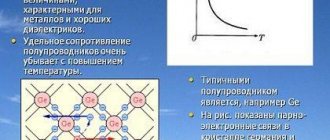
Germanium atoms have four weakly bound electrons in their outer shell. They are called valence electrons. In a crystal lattice, each atom is surrounded by its four nearest neighbors. The bond between atoms in a germanium crystal is covalent, that is, it is carried out by pairs of valence electrons. Each valence electron belongs to two atoms (Fig. 1.13.2). Valence electrons in a germanium crystal are much more strongly bound to atoms than in metals; Therefore, the concentration of conduction electrons at room temperature in semiconductors is many orders of magnitude lower than in metals. Near absolute zero temperature in a germanium crystal, all electrons are occupied in the formation of bonds. Such a crystal does not conduct electric current.
| Figure 1.13.2. Pair-electron bonds in a germanium crystal and the formation of an electron-hole pair |
As the temperature increases, some of the valence electrons may gain enough energy to break covalent bonds. Then free electrons (conduction electrons) will appear in the crystal. At the same time, vacancies are formed in places where bonds are broken, which are not occupied by electrons. These vacancies are called holes. The vacant place can be occupied by a valence electron from a neighboring pair, then the hole will move to a new place in the crystal. At a given semiconductor temperature, a certain number of electron-hole pairs are formed per unit time. At the same time, the reverse process occurs - when a free electron meets a hole, the electronic bond between the germanium atoms is restored. This process is called recombination. Electron-hole pairs can also be created when a semiconductor is illuminated due to the energy of electromagnetic radiation. In the absence of an electric field, conduction electrons and holes participate in chaotic thermal motion.
If a semiconductor is placed in an electric field, then not only free electrons are involved in the ordered movement, but also holes, which behave like positively charged particles. Therefore, the current I in a semiconductor consists of the electron In and hole currents Ip:
| I = In + Ip. |
The concentration of conduction electrons in a semiconductor is equal to the concentration of holes: nn = np. The electron-hole conductivity mechanism manifests itself only in pure (i.e., without impurities) semiconductors. It is called the intrinsic electrical conductivity of semiconductors.
In the presence of impurities, the electrical conductivity of semiconductors changes greatly. For example, adding phosphorus impurities in an amount of 0.001 atomic percent to a silicon crystal reduces the resistivity by more than five orders of magnitude. Such a strong influence of impurities can be explained on the basis of the above ideas about the structure of semiconductors.
A necessary condition for a sharp decrease in the resistivity of a semiconductor upon the introduction of impurities is the difference in the valence of the impurity atoms from the valence of the main atoms of the crystal.
The conductivity of semiconductors in the presence of impurities is called impurity conductivity. There are two types of impurity conductivity – electronic and hole.
Electronic conductivity occurs when pentavalent atoms (for example, arsenic, As) are introduced into a germanium crystal with tetravalent atoms.
| Figure 1.13.3. An arsenic atom in a germanium lattice. n-type semiconductor |
In Fig. Figure 1.13.3 shows a pentavalent arsenic atom found in a site of the germanium crystal lattice. The four valence electrons of the arsenic atom are included in the formation of covalent bonds with four neighboring germanium atoms. The fifth valence electron turned out to be redundant; it easily breaks away from the arsenic atom and becomes free. An atom that has lost an electron becomes a positive ion located at a site in the crystal lattice. An impurity of atoms with a valence exceeding the valence of the main atoms of a semiconductor crystal is called a donor impurity. As a result of its introduction, a significant number of free electrons appear in the crystal. This leads to a sharp decrease in the resistivity of the semiconductor - thousands and even millions of times. The resistivity of a conductor with a high content of impurities may approach that of a metal conductor.
In a germanium crystal with an admixture of arsenic, there are electrons and holes responsible for the crystal’s own conductivity. But the main type of free charge carriers are electrons detached from arsenic atoms. In such a crystal nn >> np. Such conductivity is called electronic conductivity, and a semiconductor that has electronic conductivity is called an n-type semiconductor.
| Figure 1.13.4. An indium atom in a germanium lattice. p-type semiconductor |
Hole conduction occurs when trivalent atoms (for example, indium atoms, In) are introduced into a germanium crystal. In Fig. Figure 1.13.4 shows an indium atom that, with the help of its valence electrons, has created covalent bonds with only three neighboring germanium atoms. The indium atom does not have an electron to form a bond with the fourth germanium atom. This missing electron can be captured by the indium atom from the covalent bond of neighboring germanium atoms. In this case, the indium atom turns into a negative ion located at a site of the crystal lattice, and a vacancy is formed in the covalent bond of neighboring atoms. An impurity of atoms capable of capturing electrons is called an acceptor impurity. As a result of the introduction of an acceptor impurity, many covalent bonds are broken in the crystal and vacancies (holes) are formed. Electrons from neighboring covalent bonds can jump to these places, which leads to chaotic wandering of holes throughout the crystal.
The presence of an acceptor impurity sharply reduces the resistivity of the semiconductor due to the appearance of a large number of free holes. The concentration of holes in a semiconductor with an acceptor impurity significantly exceeds the concentration of electrons that arose due to the mechanism of the semiconductor’s own electrical conductivity: np >> nn. This type of conductivity is called hole conductivity. An impurity semiconductor with hole conductivity is called a p-type semiconductor. The main free charge carriers in p-type semiconductors are holes.
It should be emphasized that hole conductivity is actually due to the relay movement of electrons through vacancies from one germanium atom to another, which carry out a covalent bond.
For n- and p-type semiconductors, Ohm's law is satisfied in certain ranges of current and voltage, provided that the concentrations of free carriers are constant.
Types and properties of semiconductors
All semiconductors can be divided into several main types. Among them, the leaders are pure or proprietary materials, which do not contain any impurities.
They are characterized by a crystalline structure, where the atoms are arranged in a periodic order at its nodes. Here there is a stable mutual connection between each atom and four atoms located nearby. This makes it possible to form permanent electron shells, which contain eight electrons. At a temperature equal to absolute zero, such a semiconductor becomes an insulator, since all electrons are connected by covalent bonds. When the temperature increases or any irradiation occurs, electrons can escape from covalent bonds and become free charge carriers. When moving, the free spaces are gradually occupied by other electrons, so the electric current flows only in one direction.
Electrical resistance of the conductor
Electrical resistance is a physical quantity that shows what kind of obstacle is created by the current as it passes through a conductor. The units of measurement are Ohms, in honor of Georg Ohm. In his law, he derived a formula for finding resistance, which is given below.
Let's consider the resistance of conductors using metals as an example. Metals have an internal structure in the form of a crystal lattice. This lattice has a strict order, and its nodes are positively charged ions. Charge carriers in a metal are “free” electrons, which do not belong to a specific atom, but move randomly between lattice sites.
It is known from quantum physics that the movement of electrons in a metal is the propagation of an electromagnetic wave in a solid. That is, an electron in a conductor moves at the speed of light (practically), and it has been proven that it exhibits properties not only as a particle, but also as a wave. And the resistance of the metal arises as a result of the scattering of electromagnetic waves (that is, electrons) by thermal vibrations of the lattice and its defects. When electrons collide with nodes of a crystal lattice, part of the energy is transferred to the nodes, as a result of which energy is released. This energy can be calculated at constant current, thanks to the Joule-Lenz law - Q=I2Rt. As you can see, the greater the resistance, the more energy is released.
Resistivity
There is such an important concept as resistivity, this is the same resistance, only in a unit of length. Each metal has its own, for example, for copper it is 0.0175 Ohm*mm2/m, for aluminum it is 0.0271 Ohm*mm2/m. This means that a copper bar 1 m long and a cross-sectional area of 1 mm2 will have a resistance of 0.0175 Ohm, and the same bar, but made of aluminum, will have a resistance of 0.0271 Ohm. It turns out that the electrical conductivity of copper is higher than that of aluminum. Each metal has its own specific resistance, and the resistance of the entire conductor can be calculated using the formula
where p is the resistivity of the metal, l is the length of the conductor, s is the cross-sectional area.
Resistivity values are given in the table of metal resistivities (20°C)
| Substance | p, Ohm*mm2/2 | α,10-3 1/K |
| Aluminum | 0.0271 | 3.8 |
| Tungsten | 0.055 | 4.2 |
| Iron | 0.098 | 6 |
| Gold | 0.023 | 4 |
| Brass | 0.025-0.06 | 1 |
| Manganin | 0.42-0.48 | 0,002-0,05 |
| Copper | 0.0175 | 4.1 |
| Nickel | 0.1 | 2.7 |
| Constantan | 0.44-0.52 | 0.02 |
| Nichrome | 1.1 | 0.15 |
| Silver | 0.016 | 4 |
| Zinc | 0.059 | 2.7 |
In addition to resistivity, the table contains TCR values; more on this coefficient a little later.
Dependence of resistivity on deformation
During cold forming of metals, the metal experiences plastic deformation. During plastic deformation, the crystal lattice becomes distorted and the number of defects increases. With an increase in crystal lattice defects, the resistance to the flow of electrons through the conductor increases, therefore, the resistivity of the metal increases. For example, wire is made by drawing, which means that the metal undergoes plastic deformation, as a result of which the resistivity increases. In practice, recrystallization annealing is used to reduce resistance; this is a complex technological process, after which the crystal lattice seems to “straighten out” and the number of defects decreases, and therefore the resistance of the metal too.
When stretched or compressed, the metal experiences elastic deformation. During elastic deformation caused by stretching, the amplitudes of thermal vibrations of the crystal lattice nodes increase, therefore, electrons experience great difficulty, and in connection with this, the resistivity increases. During elastic deformation caused by compression, the amplitudes of thermal vibrations of the nodes decrease, therefore, it is easier for electrons to move, and the resistivity decreases.
Effect of temperature on resistivity
As we have already found out above, the cause of resistance in metal is the nodes of the crystal lattice and their vibrations. So, as the temperature increases, the thermal vibrations of the nodes increase, which means the resistivity also increases. There is such a value as the temperature coefficient of resistance (TCR), which shows how much the resistivity of a metal increases or decreases when heated or cooled. For example, the temperature coefficient of copper at 20 degrees Celsius is 4.1 · 10 − 3 1/degree. This means that when, for example, copper wire is heated by 1 degree Celsius, its resistivity will increase by 4.1 · 10 − 3 Ohms. The resistivity with temperature changes can be calculated using the formula
where r is the resistivity after heating, r0 is the resistivity before heating, a is the temperature coefficient of resistance, t2 is the temperature before heating, t1 is the temperature after heating.
Substituting our values, we get: r=0.0175*(1+0.0041*(154-20))=0.0271 Ohm*mm2/m. As you can see, our copper bar with a length of 1 m and a cross-sectional area of 1 mm2, after heating to 154 degrees, would have the same resistance as the same bar, only made of aluminum and at a temperature of 20 degrees Celsius.
The property of changing resistance with temperature changes is used in resistance thermometers. These devices can measure temperature based on resistance readings. Resistance thermometers have high measurement accuracy, but small temperature ranges.
In practice, the properties of conductors to prevent the passage of current are used very widely. An example is an incandescent lamp, where a tungsten filament is heated due to the high resistance of the metal, its large length and narrow cross-section. Or any heating device where the coil heats up due to high resistance. In electrical engineering, an element whose main property is resistance is called a resistor. A resistor is used in almost any electrical circuit.
Exercise
An overhead three-wire line of length L is made of wire, the brand of which is given in Table 2.1. It is necessary to find the value indicated by the sign “?”, using the given example and selecting the option with the data specified in it from Table 2.1.
It should be noted that the problem, unlike the example, involves calculations related to one line wire. In brands of bare wires, the letter indicates the material of the wire (A - aluminum; M - copper), and the number indicates the cross-section of the wire in mm
| Line length L, km | Wire brand | Wire temperature T, °C | Wire resistance RT at temperature T, Ohm |
The study of the topic material ends with work with tests No. 2 (TOE-
ETM/PM” and No. 3 (TOE – ETM/IM)
The kinetic energy of atoms and ions increases, they begin to oscillate more strongly around equilibrium positions, and electrons do not have enough space for free movement.
How does the resistivity of a conductor depend on its temperature? In what units is the temperature coefficient of resistance measured?
The resistivity of conductors increases linearly with increasing temperature according to the law.
How can we explain the linear dependence of the resistivity of a conductor on temperature?
The resistivity of a conductor depends linearly on the frequency of collisions of electrons with atoms and ions of the crystal lattice, and this frequency depends on temperature.
Why does the resistivity of semiconductors decrease with increasing temperature?
As the temperature increases, the number of free electrons increases, and as the number of charge carriers increases, the resistance of the semiconductor decreases.
Based on the type of conductivity, semiconductors are divided into n-type and p-type
n-type semiconductor
Based on the type of conductivity, semiconductors are divided into n-type and p-type.
An n-type semiconductor has an impurity nature and conducts electric current like metals. Impurity elements that are added to semiconductors to produce n-type semiconductors are called donor elements. The term "n-type" comes from the word "negative", which refers to the negative charge carried by a free electron.
The theory of the charge transfer process is described as follows:
An impurity element, pentavalent As arsenic, is added to tetravalent Si silicon. During the interaction, each arsenic atom enters into a covalent bond with silicon atoms. But a fifth free arsenic atom remains, which has no place in saturated valence bonds, and it moves to a distant electron orbit, where less energy is needed to remove an electron from the atom. The electron breaks away and becomes free, capable of carrying charge. Thus, charge transfer is carried out by an electron, not a hole, that is, this type of semiconductor conducts electric current like metals. Antimony Sb also improves the properties of one of the most important semiconductors - germanium Ge.
p-type semiconductor
A p-type semiconductor, in addition to the impurity base, is characterized by the hole nature of conductivity. The impurities that are added in this case are called acceptor impurities. “p-type” comes from the word “positive,” which refers to the positive charge of the majority carriers. For example, a small amount of trivalent indium atoms is added to a semiconductor, tetravalent Si silicon. In our case, indium will be an impurity element, the atoms of which establish a covalent bond with three neighboring silicon atoms. But silicon has one free bond while the indium atom does not have a valence electron, so it captures a valence electron from the covalent bond between neighboring silicon atoms and becomes a negatively charged ion, forming a so-called hole and, accordingly, a hole transition. According to the same scheme, In ndium imparts hole conductivity to Ge germanium.
Investigating the properties of semiconductor elements and materials, studying the properties of contact between a conductor and a semiconductor, experimenting in the manufacture of semiconductor materials, O.V. Losev created the prototype of the modern LED in the 1920s.