Types and properties of semiconductors
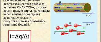
In order for an electric current to appear, there must be mobile particles that carry charges. The electrical conductivity of a substance depends on the number of such carriers per unit volume. In dielectrics they are practically absent, and in semiconductors free carriers are present only in small quantities. Consequently, the resistivity of semiconductors is very high, and in dielectrics it is even higher. There are different types of these materials, each with their own specific properties.
All semiconductors can be divided into several main types. Among them, the leaders are pure or proprietary materials, which do not contain any impurities.
They are characterized by a crystalline structure, where the atoms are arranged in a periodic order at its nodes. Here there is a stable mutual connection between each atom and four atoms located nearby. This makes it possible to form permanent electron shells, which contain eight electrons. At a temperature equal to absolute zero, such a semiconductor becomes an insulator, since all electrons are connected by covalent bonds.
When the temperature increases or any irradiation occurs, electrons can escape from covalent bonds and become free charge carriers. When moving, the free spaces are gradually occupied by other electrons, so the electric current flows only in one direction.
In electronic semiconductors, in addition to the four atoms that form the basis of the crystal lattice, there are so-called donors. They are impurities in the form of pentavalent atoms. The electron contained in such an atom cannot normally enter into a covalent bond and is therefore separated from the donor. Thus, it turns into a free charge carrier. In turn, the donor becomes a positive ion, this can happen even at room temperature.
Basics of Semiconductor Materials
If, as a sign of the classification of materials used for the manufacture of elements of electronic devices, we take their ability to conduct electric current (electrical conductivity), then all these materials, taking into account their electrical resistivity , can be divided into three groups: conductors
,
semiconductors
and
dielectrics
.
To the conductors
include materials whose electrical resistivity at room temperature (
T
= 300 K) does not exceed 10-4 Ohm×cm.
The electrical resistivity of dielectrics
is usually more than 109 Ohm×cm.
Semiconductor materials are of particular interest
. For different semiconductor materials, their electrical resistivity can be in the range from 10-4 to 109 Ohm×cm. Moreover, unlike conductors, the conductivity of semiconductors increases with increasing temperature. The number of materials with semiconductor properties exceeds the number of conductors and dielectrics. In practice, silicon, germanium, gallium arsenide, selenium, various oxides, sulfides, nitrides, etc. are most often used.
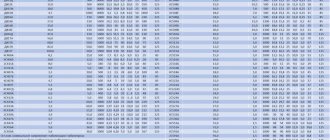
Table 1.1 shows, as an example, the values of electrical resistivity of representatives of different groups of materials at temperature T
= 300 K (
t
o = +27o C).
In terms of their ability to conduct electric current and the dependence of electrical conductivity on temperature, semiconductors are much closer to dielectrics than to conductors. This is due, first of all, to the structural features of the atoms of semiconductor materials.
As you know, an atom of any substance consists of a positively charged nucleus and negatively charged electrons moving around it. The nucleus, in turn, consists of electrically neutral particles - neutrons
and positively charged
protons
(a positive charge to a proton and a negative charge to an electron are conditionally assigned).
The negative charge of an electron ( qe
» 1.6×10⁻¹⁹ C) is equal in magnitude to the positive charge of a proton, therefore, under normal conditions, the atom is electrically neutral, since the number of protons in the nucleus is equal to the number of electrons forming the electron shell of the atom.
Table 1.1
| Materials | r, Ohm × cm | |
| Conductors: | aluminum | 2, 63 × 10-6 |
| iron | 5, 30 × 10-6 | |
| gold | 2, 44 × 10-6 | |
| copper | 1, 72 × 10-6 | |
| silver | 1, 62 × 10-6 | |
| Semiconductors: | germanium | |
| silicon | 230 × 103 | |
| gallium arsenide | 4 × 10⁸ | |
| Dielectrics: | amber | 5 × 10¹⁶ |
| mica | 1, 3 × 10¹⁴ | |
| glass | 1 × 10¹⁴ |
Electrons are in constant motion at some distance from the nucleus within layers ( shells ) determined by their energy W
.
The farther a spinning electron is from the nucleus, the higher its energy (or, as they say, energy level
) (Figure 1.1) and the weaker its connection with the atom. This means that under certain conditions (increased temperature, exposure to an external electric field, radiation, etc.), such electrons can break bonds with their atoms and become free.
The number of electrons in the layers is strictly defined: in the layer closest to the nucleus there can be no more than two electrons, in the second layer - no more than eight electrons, etc. The outer layer in the general case can be empty, so it easily gives up “its” and accepts "foreign" electrons. The electrons in the outer layer determine the valence
element in chemical reactions.
Such electrons are called valence electrons
, and they ensure the connection of atoms into molecules or crystals. This occurs due to the interaction between neighboring atoms, which consists in the fact that the electrons of one atom are affected by the nuclei of neighboring atoms. As a result of this interaction, the allowed energy levels of electrons are shifted and split into several - according to the number of neighboring atoms in the crystal lattice.
Figure 1.1 – Simplified band structure of a solid
The set of energy levels, each of which can contain electrons, is called the allowed band
(Figure 1.1).
The allowed band is characterized by the fact that all its energy levels at a temperature of 0 K are filled with electrons. The collection of energy levels corresponding to the outer layer of electrons forms the valence band
.
The allowed energy levels that remain unoccupied by electrons (at a temperature other than 0 K) constitute the conduction band
.
The gap between the valence band and the conduction band is called the band gap
.
In conductors (for example, metals), the valence band and conduction band mutually overlap (Figure 1.2, a
), therefore, valence electrons have the ability to move from the shell of one atom of a substance to the shell of another atom, performing chaotic thermal movement in the absence of an external electric field. In this regard, even at 0 K, conductors are conductive. In the presence of an external electric field, the movement of electrons becomes ordered (directed).
a B C
Figure 1.2 – Energy bands of a conductor (a), dielectric (b)
and semiconductor (c)
The number of free electrons in metals is quite large and practically independent of temperature. However, with increasing temperature, the number of collisions of electrons during their thermal movement increases, and therefore the electrical conductivity of metals decreases.
Dielectrics have a bandgap of 3
(Figure 1.2,
b
) is large (D
W
> 6 eV), the electrons of the outer shell are quite tightly bound to the nucleus and for the valence electrons to move to the conduction band, they need to be given significant energy.
So, for example, at high external electric field strength, the separation of valence electrons and their avalanche multiplication, which is called dielectric breakdown
. As a result of breakdown, the dielectric loses its properties and becomes a conductor.
Semiconductors have a band gap (Figure 1.2, in
) is relatively small and its width D
W
at a temperature of 300 K ranges from 0.1 to 3.5 eV.
Chemically pure semiconductors at absolute zero temperature ( T
= 0 K) behave in the same way as dielectrics, and their electrical conductivity is zero, since their conduction band is empty under these conditions.
To ensure the transition of semiconductor electrons from the valence band to the conduction band (that is, to make the semiconductor electrically conductive), it is necessary to somehow impart additional energy to the electrons equal to the band gap D W
.
At a temperature of 300 K, in particular, for germanium D W
= 0.66 eV, for silicon D
W
= 1.12 eV, for gallium arsenide D
W
= 1.43 eV, for silicon carbide D
W
= 2.4 ... 3 .4 eV.
The band gap of semiconductors changes with temperature. This happens as a result:
— changes in the amplitude of thermal vibrations of atoms of the crystal lattice;
— changes in interatomic distances (as a result of changes in the volume of the body).
For most semiconductors, the band gap decreases with increasing temperature.
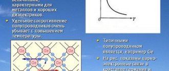
If we consider the structure of a semiconductor material at the molecular level, we can note that semiconductors are characterized by covalent bonds between individual atoms in the molecule. They are formed by adding valence electrons from neighboring atoms. For example, in the crystal lattice of a tetravalent semiconductor (germanium, silicon (Figure 1.3)), each atom is connected to four neighboring atoms using two valence electrons - one from each atom.
Figure 1.3 – Structure of the crystal lattice of a semiconductor
In an absolutely pure semiconductor, at a temperature close to absolute zero and in the absence of an external electric field, all valence electrons participate in covalent bonds. In this case, the transition of any electron from one atom to another is accompanied by a counter transition of an electron from another atom. There are no free charge carriers, therefore the electrical conductivity of a semiconductor under such conditions is zero, its properties are close to the properties of a dielectric.
Under the influence of external factors (for example, with increasing temperature, in the presence of an external electric field), thermal vibrations of atoms in the crystal lattice of a chemically pure semiconductor lead to an increase in the energy of valence electrons, which can break away from “their” atoms and begin to move freely. Therefore, at normal room temperature, semiconductors, unlike dielectrics, have some electrical conductivity. With increasing temperature, the number of detached electrons increases, and, consequently, the electrical conductivity of the semiconductor increases. Electrical conductivity of a semiconductor due to the formation of charge carriers under the influence of temperature
, is called
intrinsic electrical conductivity .
When a covalent bond is broken, a vacant place is formed in the structure of the molecule - a “ hole”
» at the atom from which the electron was “torn off”.
The valence electron of any neighboring atom can move to the vacant place. In turn, an electron from another atom moves to the place vacated after the departure of the second electron, etc. The movement of electrons in a chain of such transitions occurs sequentially - each electron moves to the place vacated after its predecessor. In the direction opposite to the movement of electrons, vacant places – “holes” – also move sequentially. Thus, in a semiconductor there are two types of charge carriers - electrons
and
holes
. The hole is assigned a positive charge, numerically equal to the charge of the electron.
The process of formation of an electron-hole pair under the influence of temperature is called thermal generation .
An electron that leaves an atom during thermal generation and destroys a covalent bond can remain in a free state for a very short time. As it moves, it eventually enters the hole zone and fills the vacated covalent bond in another atom. In this case, the previously broken covalent bond is restored, and the electron and hole disappear - the electron is “captured” by the hole or the hole is “occupied” by the electron. This process is called recombination
.
At a certain temperature of a semiconductor material, there is a thermodynamic equilibrium between generation and recombination, as a result of which a certain concentration of free charge carriers: electrons and holes is established in the semiconductor. Moreover, in a pure semiconductor they always form and disappear in pairs, that is, the number of electrons and holes in it is always the same. The average lifetime of an electron-hole pair is called the charge carrier lifetime .
In the absence of an external electric field, the electron and hole, which appear as a result of thermal generation, perform chaotic movements in the volume of the semiconductor, which do not lead to a displacement of electrons in one direction, i.e., do not contribute to the appearance of an electric current in the semiconductor. If a semiconductor is placed in an electric field, then the movements of electrons and holes become directional - free charge carriers drift, which causes the appearance of an electric current in the semiconductor, which is called drift
.
In this case, the electrical conductivity of a semiconductor is determined by two types of charge carriers: electrons and holes.
The drift current in a semiconductor depends on the concentration of charge carriers and their mobility. In a pure semiconductor, as the temperature increases, the concentration of mobile carriers increases, and, consequently, the conductivity increases.
In addition to the drift current in semiconductors, there is a so-called diffusion current, which arises as a result of an uneven concentration of charge carriers in the semiconductor crystal.
Despite the presence of two types of currents in semiconductors - drift and diffusion, their own electrical conductivity remains insignificant even at elevated temperatures. Therefore, pure semiconductor material is not used for the manufacture of electronic components.
Impurity materials are used to create semiconductor devices.
semiconductors.
an impurity
is added to the semiconductor material (approximately one impurity atom per 106 ... 108 atoms of the main substance).
There are two types of impurities: acceptor
and
donor
.
If a semiconductor material of the fourth group of the periodic table (for example, silicon Si) is added as an impurity to a material from the fifth group (for example, phosphorus P, arsenic As, antimony Sb), then the four valence electrons of the impurity form covalent bonds with the four valence electrons of the semiconductor ( one from each of the four atoms of the base material), and the fifth valence electron of the impurity does not form such a bond, i.e., electric charge carriers appear - free electrons
, which can freely move throughout the volume of the semiconductor (Figure 1.4,
a
).
Figure 1.4 – Structure of a semiconductor crystal enriched
with donor ( a
) and acceptor (
b
) impurity
The electrical conductivity of a semiconductor, due to the presence of free electrons, is called n-type electrical conductivity
, and a semiconductor that realizes
n
-type electrical conductivity is called
an n-type semiconductor.
The impurity that causes
n
-type electrical conductivity is called
donor
.
When a free electron is formed, the impurity atom acquires a positive charge and becomes an immobile ion
.
If a material the third group is added as an impurity to a semiconductor material of the fourth group of the periodic table (for example, indium In, boron B, aluminum Al), then three valence electrons of the impurity form covalent bonds with three valence electrons of the semiconductor. The missing valence electron to form a covalent bond is easily attracted by an impurity atom from one of the neighboring semiconductor atoms. At the site of the broken covalent bond, a positive electric charge carrier (hole) is formed, and the impurity atom acquires a negative charge and becomes an immobile ion
(Figure 1.4,
b
).
The electrical conductivity of a semiconductor due to free holes is called electrical conductivity p
-
type
, and a semiconductor that realizes
p
-type electrical conductivity is called
a p
-
type
.
The impurity that causes p
-type electrical conductivity is called
acceptor
(receiving).
The charge carriers resulting from the addition of an impurity to the semiconductor quantitatively predominate over the charge carriers resulting from the thermal generation process, therefore the electrons in the semiconductor are
-type and holes in a
p
-type semiconductor are called
the main charge carriers
(we will denote
pp
and
pp,
respectively).
In turn, electrons in a p
-type semiconductor and holes in an
n
-type semiconductor are
minority charge carriers
(
pr
and
pn
, respectively).
If, as a sign of the classification of materials used for the manufacture of elements of electronic devices, we take their ability to conduct electric current (electrical conductivity), then all these materials, taking into account their electrical resistivity , can be divided into three groups: conductors
,
semiconductors
and
dielectrics
.
To the conductors
include materials whose electrical resistivity at room temperature (
T
= 300 K) does not exceed 10-4 Ohm×cm.
The electrical resistivity of dielectrics
is usually more than 109 Ohm×cm.
Semiconductor materials are of particular interest
. For different semiconductor materials, their electrical resistivity can be in the range from 10-4 to 109 Ohm×cm. Moreover, unlike conductors, the conductivity of semiconductors increases with increasing temperature. The number of materials with semiconductor properties exceeds the number of conductors and dielectrics. In practice, silicon, germanium, gallium arsenide, selenium, various oxides, sulfides, nitrides, etc. are most often used.
Table 1.1 shows, as an example, the values of electrical resistivity of representatives of different groups of materials at temperature T
= 300 K (
t
o = +27o C).
In terms of their ability to conduct electric current and the dependence of electrical conductivity on temperature, semiconductors are much closer to dielectrics than to conductors. This is due, first of all, to the structural features of the atoms of semiconductor materials.
As you know, an atom of any substance consists of a positively charged nucleus and negatively charged electrons moving around it. The nucleus, in turn, consists of electrically neutral particles - neutrons
and positively charged
protons
(a positive charge to a proton and a negative charge to an electron are conditionally assigned).
The negative charge of an electron ( qe
» 1.6×10⁻¹⁹ C) is equal in magnitude to the positive charge of a proton, therefore, under normal conditions, the atom is electrically neutral, since the number of protons in the nucleus is equal to the number of electrons forming the electron shell of the atom.
Table 1.1
| Materials | r, Ohm × cm | |
| Conductors: | aluminum | 2, 63 × 10-6 |
| iron | 5, 30 × 10-6 | |
| gold | 2, 44 × 10-6 | |
| copper | 1, 72 × 10-6 | |
| silver | 1, 62 × 10-6 | |
| Semiconductors: | germanium | |
| silicon | 230 × 103 | |
| gallium arsenide | 4 × 10⁸ | |
| Dielectrics: | amber | 5 × 10¹⁶ |
| mica | 1, 3 × 10¹⁴ | |
| glass | 1 × 10¹⁴ |
Electrons are in constant motion at some distance from the nucleus within layers ( shells ) determined by their energy W
.
The farther a spinning electron is from the nucleus, the higher its energy (or, as they say, energy level
) (Figure 1.1) and the weaker its connection with the atom. This means that under certain conditions (increased temperature, exposure to an external electric field, radiation, etc.), such electrons can break bonds with their atoms and become free.
The number of electrons in the layers is strictly defined: in the layer closest to the nucleus there can be no more than two electrons, in the second layer - no more than eight electrons, etc. The outer layer in the general case can be empty, so it easily gives up “its” and accepts "foreign" electrons. The electrons in the outer layer determine the valence
element in chemical reactions.
Such electrons are called valence electrons
, and they ensure the connection of atoms into molecules or crystals. This occurs due to the interaction between neighboring atoms, which consists in the fact that the electrons of one atom are affected by the nuclei of neighboring atoms. As a result of this interaction, the allowed energy levels of electrons are shifted and split into several - according to the number of neighboring atoms in the crystal lattice.
Figure 1.1 – Simplified band structure of a solid
The set of energy levels, each of which can contain electrons, is called the allowed band
(Figure 1.1).
The allowed band is characterized by the fact that all its energy levels at a temperature of 0 K are filled with electrons. The collection of energy levels corresponding to the outer layer of electrons forms the valence band
.
The allowed energy levels that remain unoccupied by electrons (at a temperature other than 0 K) constitute the conduction band
.
The gap between the valence band and the conduction band is called the band gap
.
In conductors (for example, metals), the valence band and conduction band mutually overlap (Figure 1.2, a
), therefore, valence electrons have the ability to move from the shell of one atom of a substance to the shell of another atom, performing chaotic thermal movement in the absence of an external electric field. In this regard, even at 0 K, conductors are conductive. In the presence of an external electric field, the movement of electrons becomes ordered (directed).
a B C
Figure 1.2 – Energy bands of a conductor (a), dielectric (b)
and semiconductor (c)
The number of free electrons in metals is quite large and practically independent of temperature. However, with increasing temperature, the number of collisions of electrons during their thermal movement increases, and therefore the electrical conductivity of metals decreases.
Dielectrics have a bandgap of 3
(Figure 1.2,
b
) is large (D
W
> 6 eV), the electrons of the outer shell are quite tightly bound to the nucleus and for the valence electrons to move to the conduction band, they need to be given significant energy.
So, for example, at high external electric field strength, the separation of valence electrons and their avalanche multiplication, which is called dielectric breakdown
. As a result of breakdown, the dielectric loses its properties and becomes a conductor.
Semiconductors have a band gap (Figure 1.2, in
) is relatively small and its width D
W
at a temperature of 300 K ranges from 0.1 to 3.5 eV.
Chemically pure semiconductors at absolute zero temperature ( T
= 0 K) behave in the same way as dielectrics, and their electrical conductivity is zero, since their conduction band is empty under these conditions.
To ensure the transition of semiconductor electrons from the valence band to the conduction band (that is, to make the semiconductor electrically conductive), it is necessary to somehow impart additional energy to the electrons equal to the band gap D W
.
At a temperature of 300 K, in particular, for germanium D W
= 0.66 eV, for silicon D
W
= 1.12 eV, for gallium arsenide D
W
= 1.43 eV, for silicon carbide D
W
= 2.4 ... 3 .4 eV.
The band gap of semiconductors changes with temperature. This happens as a result:
— changes in the amplitude of thermal vibrations of atoms of the crystal lattice;
— changes in interatomic distances (as a result of changes in the volume of the body).
For most semiconductors, the band gap decreases with increasing temperature.
If we consider the structure of a semiconductor material at the molecular level, we can note that semiconductors are characterized by covalent bonds between individual atoms in the molecule. They are formed by adding valence electrons from neighboring atoms. For example, in the crystal lattice of a tetravalent semiconductor (germanium, silicon (Figure 1.3)), each atom is connected to four neighboring atoms using two valence electrons - one from each atom.
Figure 1.3 – Structure of the crystal lattice of a semiconductor
In an absolutely pure semiconductor, at a temperature close to absolute zero and in the absence of an external electric field, all valence electrons participate in covalent bonds. In this case, the transition of any electron from one atom to another is accompanied by a counter transition of an electron from another atom. There are no free charge carriers, therefore the electrical conductivity of a semiconductor under such conditions is zero, its properties are close to the properties of a dielectric.
Under the influence of external factors (for example, with increasing temperature, in the presence of an external electric field), thermal vibrations of atoms in the crystal lattice of a chemically pure semiconductor lead to an increase in the energy of valence electrons, which can break away from “their” atoms and begin to move freely. Therefore, at normal room temperature, semiconductors, unlike dielectrics, have some electrical conductivity. With increasing temperature, the number of detached electrons increases, and, consequently, the electrical conductivity of the semiconductor increases. Electrical conductivity of a semiconductor due to the formation of charge carriers under the influence of temperature
, is called
intrinsic electrical conductivity .
When a covalent bond is broken, a vacant place is formed in the structure of the molecule - a “ hole”
» at the atom from which the electron was “torn off”.
The valence electron of any neighboring atom can move to the vacant place. In turn, an electron from another atom moves to the place vacated after the departure of the second electron, etc. The movement of electrons in a chain of such transitions occurs sequentially - each electron moves to the place vacated after its predecessor. In the direction opposite to the movement of electrons, vacant places – “holes” – also move sequentially. Thus, in a semiconductor there are two types of charge carriers - electrons
and
holes
. The hole is assigned a positive charge, numerically equal to the charge of the electron.
The process of formation of an electron-hole pair under the influence of temperature is called thermal generation .
An electron that leaves an atom during thermal generation and destroys a covalent bond can remain in a free state for a very short time. As it moves, it eventually enters the hole zone and fills the vacated covalent bond in another atom. In this case, the previously broken covalent bond is restored, and the electron and hole disappear - the electron is “captured” by the hole or the hole is “occupied” by the electron. This process is called recombination
.
At a certain temperature of a semiconductor material, there is a thermodynamic equilibrium between generation and recombination, as a result of which a certain concentration of free charge carriers: electrons and holes is established in the semiconductor. Moreover, in a pure semiconductor they always form and disappear in pairs, that is, the number of electrons and holes in it is always the same. The average lifetime of an electron-hole pair is called the charge carrier lifetime .
In the absence of an external electric field, the electron and hole, which appear as a result of thermal generation, perform chaotic movements in the volume of the semiconductor, which do not lead to a displacement of electrons in one direction, i.e., do not contribute to the appearance of an electric current in the semiconductor. If a semiconductor is placed in an electric field, then the movements of electrons and holes become directional - free charge carriers drift, which causes the appearance of an electric current in the semiconductor, which is called drift
.
In this case, the electrical conductivity of a semiconductor is determined by two types of charge carriers: electrons and holes.
The drift current in a semiconductor depends on the concentration of charge carriers and their mobility. In a pure semiconductor, as the temperature increases, the concentration of mobile carriers increases, and, consequently, the conductivity increases.
In addition to the drift current in semiconductors, there is a so-called diffusion current, which arises as a result of an uneven concentration of charge carriers in the semiconductor crystal.
Despite the presence of two types of currents in semiconductors - drift and diffusion, their own electrical conductivity remains insignificant even at elevated temperatures. Therefore, pure semiconductor material is not used for the manufacture of electronic components.
Impurity materials are used to create semiconductor devices.
semiconductors.
an impurity
is added to the semiconductor material (approximately one impurity atom per 106 ... 108 atoms of the main substance).
There are two types of impurities: acceptor
and
donor
.
If a semiconductor material of the fourth group of the periodic table (for example, silicon Si) is added as an impurity to a material from the fifth group (for example, phosphorus P, arsenic As, antimony Sb), then the four valence electrons of the impurity form covalent bonds with the four valence electrons of the semiconductor ( one from each of the four atoms of the base material), and the fifth valence electron of the impurity does not form such a bond, i.e., electric charge carriers appear - free electrons
, which can freely move throughout the volume of the semiconductor (Figure 1.4,
a
).
Figure 1.4 – Structure of a semiconductor crystal enriched
with donor ( a
) and acceptor (
b
) impurity
The electrical conductivity of a semiconductor, due to the presence of free electrons, is called n-type electrical conductivity
, and a semiconductor that realizes
n
-type electrical conductivity is called
an n-type semiconductor.
The impurity that causes
n
-type electrical conductivity is called
donor
.
When a free electron is formed, the impurity atom acquires a positive charge and becomes an immobile ion
.
If a material the third group is added as an impurity to a semiconductor material of the fourth group of the periodic table (for example, indium In, boron B, aluminum Al), then three valence electrons of the impurity form covalent bonds with three valence electrons of the semiconductor. The missing valence electron to form a covalent bond is easily attracted by an impurity atom from one of the neighboring semiconductor atoms. At the site of the broken covalent bond, a positive electric charge carrier (hole) is formed, and the impurity atom acquires a negative charge and becomes an immobile ion
(Figure 1.4,
b
).
The electrical conductivity of a semiconductor due to free holes is called electrical conductivity p
-
type
, and a semiconductor that realizes
p
-type electrical conductivity is called
a p
-
type
.
The impurity that causes p
-type electrical conductivity is called
acceptor
(receiving).
The charge carriers resulting from the addition of an impurity to the semiconductor quantitatively predominate over the charge carriers resulting from the thermal generation process, therefore the electrons in the semiconductor are
-type and holes in a
p
-type semiconductor are called
the main charge carriers
(we will denote
pp
and
pp,
respectively).
In turn, electrons in a p
-type semiconductor and holes in an
n
-type semiconductor are
minority charge carriers
(
pr
and
pn
, respectively).
Factors affecting the resistance of semiconductors
It has been experimentally established that as the temperature increases, the electrical resistance in semiconductor crystals decreases. This is due to the fact that when the crystal is heated, the number of free electrons increases, and their concentration increases accordingly. The changing resistance of semiconductors under the influence of temperature is used to create special devices called thermistors.
In order to make a thermistor, semiconductors are used, which are oxides of individual metals in a mixed state. The finished substance is placed in a protective metal case with insulated terminals. With their help, the device is connected to the electrical circuit.
Thermistors are used to measure temperature or to maintain it in a given mode in any devices. The main principle of their operation is changing resistance with temperature changes. The same principle is used in photoresistors. Here the resistance value changes depending on the lighting level.