Home > Theory > RS trigger
The basic building block that makes computer memory possible, and is also used in many sequential logic devices, is the flip-flop, or bistable, circuit. Only two interconnected logic inputs constitute the basic form of this circuit, the output of which has two stable states. When the circuit is driven into any of these by a suitable input pulse, it will "remember" that state until it is changed by an additional input pulse, or until the power is turned off.
Logic chip
Classification of sequential circuits
Sequential circuits can be used for simple flip-flops or to create more complex systems: memory devices, counters, shift registers. They are divided into three main categories:
- Asynchronous, changing status when turned on;
- Synchronous, consistent with the clock signal;
- Combined, responsive to the triggering of impulses.
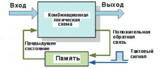
Important! If the circuit depends on an external input, then it is asynchronous. If the states change depending on the clock signal, then it is synchronous. To save the state, there is feedback when part of the signal from the output goes back to the input.
What is RS trigger
Cotton switch and its features
An RS flip-flop can be thought of as a one-bit memory because it retains the input pulse even after it has passed. Different types of flip-flops can be made from logic gates. The most commonly used are NAND and NOR. The most used ones are AND-NOT. This is due to their versatility, meaning that any of the other standard logic functions can be simulated.
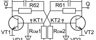
The RS (Set-Reset) trigger circuit is one of the simplest serial connections, consisting of two cross-connected valves. The output of each is connected to the input of the other, giving a form of positive feedback.
RS trigger
The PC flip-flop has two active inputs (S and R) and two outputs (Q and Q̃ (not-Q)). For synchronous circuits, an input C with a clock signal is added.
For an RS trigger, the operating principle can be described as follows:
- Installation status. Let the input of one gate R be at logical level 0, and the input of another S be at level 1. The output of the first element Q̃ is 1 (logical NAND principle). This output is simultaneously fed to the input of the first valve. As a result, both of its inputs correspond to 1, and the output Q corresponds to 0. If the input R changes to 1, and S remains at the same level of 1, then the first gate receives another 0 input via feedback, and the output Q̃ will remain unchanged - 1. The trigger circuit is locked or set with Q equal to 0 and Q̃ equal to 1, regardless of the signal applied;
- Reset state. Is an alternative unchangeable state. Its initial conditions: the logical signal level at the input of the first gate R is 1, and the second S is 0. The output Q̃ has the value 0, Q corresponds to 1. Since one of the inputs of the second gate has logic 0, the output Q is 1 ( according to the logical AND-NOT principle). Here again the feedback works, and the first gate receives a 1 as an input. Two ones at the input provide a 0 at the output Q̃. When the given logic of the input S changes to 1 and the same signal 1 is maintained at the input R, the output Q̃ remains 0, and at Q – 1. That is, a new state is fixed, independent of changes in the input value.
Important! A signal must be supplied to the S (set) input, which puts the circuit in a state where Q is equal to one. The signal at the R (reset) input resets the circuit to the zero state.
Lesson 8.4 Triggers, registers, counters
In the previous lesson, we looked at logical elements, the state of the signal at the output of which is uniquely determined by the states of the signals at the inputs.
Logic elements serve as the basis for creating more complex digital devices, one of which is a trigger. A trigger is a whole class of electronic devices that can remain in one of two stable states for a long time after the signal that changes the state has stopped. The state of the trigger's output is determined not only by the signals at its inputs, but also by the previous state of the device. Thus, a flip-flop is the simplest one-bit memory cell.
RS trigger
The simplest trigger can be obtained from two logical elements 2OR-NOT:
Circuit designation:
This circuit is an asynchronous RS flip-flop.
It has two inputs: S (set) - installation, R (reset) - reset, and two outputs: Q (direct) and Q with an overbar (inverse, NOT_Q).
When a logical zero signal is applied to both inputs of the trigger, its outputs will be set to an arbitrary state. Let's say Q = 0 and NOT_Q =1. If a “1” is applied to input S, then the state of output Q will abruptly change to “1”, and NOT_Q will change to “0”. And this state will be maintained regardless of whether “0” or “1” is applied to the S input, which is a manifestation of the memory property.
Accordingly, when the level “1” is applied to the input R, the output Q will become “0”, and NOT_Q will become “1”.
The duration of the establishing pulses can be very short, and is limited by the physical speed of the logical modules from which the trigger is built.
The situation when the R and S inputs are high is unacceptable, since the circuit cannot operate correctly. This is a disadvantage of the RS trigger.
An RS flip-flop can also be built from two NAND elements; such elements are more common:
Installation and reset of the trigger on the 2I-NOT elements, unlike the previous one, is carried out by a low level of the input signal.
If we add two more 2I-NOT gates to the last circuit, we get a synchronous RS flip-flop.
The state of such a trigger changes only when input C (Clock) is exposed to a synchronizing (clock) pulse.
D-trigger
By slightly changing the circuit of a synchronous RS flip-flop, you can get a D flip-flop. (D-delay, delay). It has only one information input D.
If a “1” is applied to this input and then a pulse is applied to input C, then the output Q will be “1”; if a “0” is applied to the input, then a pulse is applied to C, then the output Q will be “0”. Thus, the D-flip-flop delays the information arriving at the input.
If input D is connected to output NOT_Q, then the trigger will change its state every time the state of input C changes from “0” to “1”. When changing from "1" to "0", the state of the trigger will not change. Thus, the frequency of the output pulses will be half the frequency of the input pulses. Such a flip-flop is called a counting or T-flip-flop. The frequency divider is used very widely in digital technology.
There is a type of synchronous RS flip-flop that does not have a prohibited combination - a JK flip-flop. It has three inputs: J (instead of R), K (instead of S), and C. If “1” is applied to both information inputs, then the JK flip-flop operates as a counting T flip-flop with input C.
Storage register
More complex digital devices, such as registers, can be built using flip-flops. Registers are designed to store multi-bit information, that is, numbers written in binary code.
Consider a three-bit storage register on D flip-flops:
Each flip-flop can store one digit (bit) of a number. Input R is used to set the outputs of all flip-flops to the zero (initial) state before recording a number that is supplied to inputs D0, D1 and D2. When a pulse is applied to input C, information is recorded from these inputs. Information can be stored indefinitely as long as input C is not pulsed and power is supplied.
Shift register
Another type of register is a shift register. It is designed to transform information by bitwise shifting it in one direction or another. The following figure shows a diagram of the simplest right shift register (according to the diagram):
Unlike the storage register, the output of the previous flip-flop is connected to the input of the next one. Information in the form of a logical level is supplied to the input of the first (leftmost) flip-flop. When a pulse is applied to input C, the information present at input D is written to the first flip-flop. When the second pulse is applied, the information from the first trigger is rewritten into the second trigger, and the information that is at that moment present at input D is written into the first, and so on. Thus, with each clock pulse, the information in the register shifts to the right by 1 bit.
Shift registers are used in many circuit solutions in the construction of digital devices, primarily for converting serial code into parallel, as well as for performing arithmetic operations (multiplication and division by 2) with binary numbers, organizing delay lines, generating pulses of a given duration, generating pseudo-random sequences (codes), etc.
Counter
Another class of digital devices that can be built on flip-flops are counters. As the name suggests, they count input pulses in a given code and can store the result.
The simplest sequential carry counter can be obtained using counting T-flip-flops:
By applying a pulse to input R, the counter is brought to its initial state when outputs Q1-Q3 are at a logical zero level.
Pulses for counting are supplied to input C. With the arrival of the falling edge of the first pulse, the first (left) trigger in the circuit is set to “1”. If you read the code from right to left, it corresponds to one. For our three-digit counter, this is code 001. With the arrival of the second pulse at “1,” the second trigger switches, and the first switches to “0.” Thus, the code at the counter outputs will be 010, which corresponds to the decimal digit 2. The next pulse will set the code 011, that is, 3. A three-digit counter can count up to code 111, which corresponds to the decimal digit 7. In this case, the so-called counter overflow occurs, and with the arrival of the next pulse will reset the counter to zero.
Since the counter triggers are connected in series, they will also switch in series. This process is displayed on the graph, from which it can be seen that the switching delay time tз will double and triple. As the number of bits increases, the delay may become unacceptable, which is a disadvantage of serial carry counters.
To increase performance, counters with parallel transfer are used, which is achieved by simultaneously applying input pulses to the inputs of all counter triggers. This is realized by introducing AND logic elements into the circuit:
From the diagram it can be seen that the counting pulse will arrive at the input of the second trigger only when the output of the first trigger is “1”, and to the third - when “1” is at the outputs of both the first and second triggers. Obviously, with an increase in the number of bits, it is necessary to increase both the number of logical AND elements and the number of their inputs, which, in turn, is a disadvantage of this type of counter.
Registers and counters, in turn, can be used to build more complex digital devices: adders, RAM and ROM (random access and read-only memories), ALUs (arithmetic logic units) that are part of processors, and so on, to an increasingly complex digital devices.
In the next series of articles, we'll begin our introduction to microcontrollers, a remarkable class of digital chips that are true computers that fit on a single chip and are found in most electronic devices, from coffee machines to spaceships!
Truth table
The operation of the RS trigger can be represented in the truth table:
- Q is set to logic 1 if a 0 is applied at the S input;
- Changing the S-input by one does not affect the output logic. The 0-pulse was stored by Q;
- Q is reset to 0 by a logic 0 applied to the R input;
- When R returns to 1, Q is stored at 0.
Truth table
For the conditions of the 2nd and 3rd rows of the table, Q̃ is the inverse of Q. However, in the first row, both inputs are 0, which makes Q̃ = Q = 1, and they will not be opposite logic states. In practice, this condition is not allowed, since the RS trigger loses stability.
In the last line there is a logical one at both inputs, the outputs Q̃ and Q will be in opposite states, but it is not clear what specific values they will have. They will correspond to those stored from the last input pulse.
In addition to using NAND logic, simple flip-flops can be constructed using two cross-connected AND-OR gates. The scheme works similarly. Only the disabled state will occur when both input signals are equal to one.
Timing diagrams
Pulse duty cycle
Truth tables are sometimes not the best method for describing a sequential circuit. A timing diagram that shows how logic states at different points in a circuit change over time is often preferred.
RS flip-flop timing diagram
The figure shows that at the first time t1 both signals are high, which causes an uncertain state. Then from t1 to t2 S is 0, R is 1 and output Q is set to 1. There are two more undefined states: from t2 to t3 and from t4 to t5. In the interval t3-t4, the circuit is reset to 0 at output Q. And within t6-t7, the circuit is in an invalid state when R and S are equal to 0.
Power plants
Timing diagrams, also called pulse diagrams, are an aid to better understand the operation of a flip-flop and the entire circuit as a whole. The input timing signals are preset or can be selected as desired. The output signals depend on the input signals. Let us explain this with a simple example. In Fig. Figure 7.88 shows a non-clocked ^S'-flip-flop, the so-called LU storage flip-flop with a truth table and timing diagrams. The truth table is valid for time t.
Rice. 7.88. RS storage flip-flop with truth table for time tm and timing diagram
At time tx, the flip-flop is set, since S is acted upon by a 1-signal. At time t2, the flip-flop is reset. The output R signal is 1. At time /3, the trigger is set again. Particularly interesting is /4. From this moment on, signal 1 is active on both inputs. This combination is prohibited. Both outputs switch to 1. If at time t5 a 0 is applied to the /?-input, then Q2 will also be set to 0. At point t6, the 5-signal is 0. The trigger remains set. Reset is only possible with R = 1. At point t7 the flip-flop could be reset. However, it is not installed yet. Therefore, the output states do not change. At point ?8, the L-signal becomes equal to 1. However, it does not reach 1. Again, an incorrect combination of Qt = 1 and Q2 = 1 arises. Particularly critical is the moment t9, at which the S and R signals simultaneously decrease to 0. It becomes unclear at what point the trigger state will be set. The combination S = R - 1 is illegal and should be avoided. Let's look at Fig. 7.89. The input signals S and R and the synchronization signal T are given. At time tx S = 1, but a 0 signal is still connected to T. The trigger cannot be installed. Only at time t2 will the trigger be established. At point /3 it will reset. At point t S becomes equal to 1, and at point t R = 1.
Rice. 7.89. Clocked RS flip-flop with dominant R input, truth table and timing diagram
Since the clock signal is not turned on, these signals have no effect on the trigger. Only at point t6 do they act on the trigger. The trigger should now reset. However, it has already been reset and therefore the state of the outputs does not change. At point t7 the trigger is set. At point t% a reset occurs, since despite the single states of the S and R inputs, the 7?-input has priority. The state of the output Q2 is always in antiphase to the state of the output Qv. What timing diagram corresponds to Ql and Qv if an RS-trctor with a dominant jR-input were controlled by the leading edge of the clock pulse? The corresponding timing diagram is shown in Fig. 7.90. The flip-flop can only be switched at times tv tv ty At point tx the flip-flop will be set, since S = 1. At point t2, the flip-flop is reset, since S = R = 1. At point t3, the flip-flop will be set again (S = 1). For Qx and Q2, a completely different diagram is obtained than in Fig. 7.89.
For a single edge-controlled /YG trigger in Fig. 7.91 the following timing diagram is obtained. The trigger can only switch at times tv t2, t3, t4, ts and t6. Only at these times are the falling edges of the C-signal applied. At point tx, the trigger will be installed, since / = 1. At point tx, the trigger will be reset, since K - 1. At time t3, the trigger should have been reset, but since it has already been reset, the states of the outputs Qx and Q2 do not change. At point t4 /= 1 and K= 1. The trigger switches. Since before the moment of time Qx was equal to 0, then after t4 Qx = 1. At points ts and t6 the trigger switches to the opposite state. The state of output Q2 is always in antiphase to the state of output Qx. As the next example, consider the timing diagrams of a /A'-trigger controlled by two edges (Fig. 7.92). At point tx, the input signal / = 1 enters the master flip-flop. And only at time t2 (with the reverse edge of the clock pulse) signals corresponding to the setting mode Qx - 1 and Q2 = 0 appear at the outputs. At time G3 / = 0 and K = 0. This is the storage mode. Therefore, at point /4, the states of the outputs do not change. At point t5, the input signal K = 1 enters the leading flip-flop. But only at time t6 signals corresponding to the reset mode Qx = 0 and Q2 = 1 appear at the outputs. At time t7 J = 1 and K = 1. With this combination of input signals, the trigger will switch the outputs to states opposite to the current ones, but only at time tr At point t9 AT becomes equal to 1. The output signals are reset at point tl0.
Rice. 7.92. Double edge controlled JK flip-flop (MS flip-flop) with truth table and timing diagram
Similar articles
JK trigger
Rectifier
Other common types of logic circuits are JK, D and T, which are developments of the RS flip-flop using logic elements.
Disadvantages of the NAND-NOT RS flip-flop circuit:
- The need to avoid the condition where both input signals are 0;
- For state changes R and S that have a single input signal, the correct blocking action does not always occur.
To overcome these shortcomings, the JK flip-flop circuit was developed. Its inputs are the same R and S, but they are assigned the letters J and K after the circuit's inventor to distinguish them from other flip-flops. The JK circuit differs from the RS flip-flop in that it does not have undefined or disabled input states.
JK trigger
JK adds an input clock circuit to prevent an undefined output condition that can happen if R and S are equal to one. Therefore, there are four possible input combinations: 1, 0, “no change” and “toggle”. Input J corresponds to S, and K to R. In addition, there is a third input for each gate. The output remains Q̃ and Q.
Cross-coupling an RS flip-flop allows previously undefined flip-flop operating conditions when both inputs are 1 to be used to create a "switch" since the two inputs can be blocked.
JK circuit is SR flip- flop SET or RESET ) to be active at any time, thereby eliminating the invalid condition:
- If the SET terminal is active, the J input is blocked with status 0 (Q̃) via the lower NAND gate;
- If the RESET terminal is in effect, the K input is blocked at status 0 through the upper NAND gate.
Since Q̃ and Q are always different, they can be used to manipulate the input. For a JK flip-flop, the truth table takes the following form.
JK flip-flop truth table
When both J and K inputs are 1 at high clock, the circuit can switch from SET to RESET and vice versa.
Triggers
Triggers and registers are the simplest representatives of digital microcircuits that have internal memory. If the output signals of logic elements and combinational microcircuits are uniquely determined by their current input signals, then the output signals of microcircuits with internal memory also depend on what input signals and in what sequence arrived at them in the past, that is, they remember the history of the circuit’s behavior. That is why their use makes it possible to build much more complex and intelligent digital devices than in the case of the simplest microcircuits without memory. Microcircuits with internal memory are also called sequential or sequential, in contrast to combinational microcircuits.
Flip-flops and registers retain their memory only as long as supply voltage is applied to them. In other words, their memory is of the operational
(as opposed to
read-only memory
and
reprogrammable read-only memory
, which are not prevented from storing information by turning off the power). After turning off the power and then turning it back on, flip-flops and registers go into a random state, that is, their output signals can be set to both the logical one level and the logical zero level. This must be taken into account when designing circuits.
The big advantage of flip-flops and registers over other types of memory chips is their extremely high performance (that is, minimal response delay times and the highest permissible operating frequency). This is why flip-flops and registers are sometimes also called ultra-random access memory.
. However, the disadvantage of flip-flops and registers is that their internal memory capacity is very small; they can only store individual signals, bits (flip-flops) or individual codes, bytes, words (registers).
A flip-flop can be thought of as a single-bit memory cell, and a register as a multi-bit memory cell, which consists of several flip-flops connected in parallel (a regular, parallel register) or in series (a shift register or, which is the same thing, a shift register).
Triggers
Operating principle and types of triggers
The basis of any trigger (English - “trigger” or “flip-flop”) is a circuit of two logical elements that are covered by positive feedback (that is, signals from the outputs are fed to the inputs).
As a result of such inclusion, the circuit can be in one of two stable states, and remain indefinitely as long as the supply voltage is applied to it. Rice.
7.1. Trigger cell circuit
An example of such a circuit (the so-called trigger cell) on two two-input NAND elements is shown in Fig. 7.1. The circuit has two inverse inputs: –R – reset (from English Reset), and –S – installation (from English Set), as well as two outputs: direct output Q and inverse output –Q.
For the circuit to operate correctly, negative pulses must not arrive at its inputs simultaneously. The arrival of a pulse at the -R input turns the -Q output into a one state, and since the -S signal is one, the Q output becomes zero. The same signal Q is supplied through the feedback circuit to the input of the lower element. Therefore, even after the end of the pulse at the -R input, the state of the circuit does not change (zero remains at Q, one remains at -Q). In the same way, when a pulse arrives at the input -S, the output Q goes to one, and the output -Q goes to zero. Both of these stable states of the trigger cell can remain indefinitely until the next input pulse arrives - in other words, the circuit has memory.
If both input pulses arrive strictly simultaneously, then at the moment of action of these pulses there will be single signals at both outputs, and after the end of the input pulses the outputs will randomly fall into one of two stable states.
Similarly, one of the two stable states of the trigger cell will be randomly selected when the power is turned on. The timing diagram of the trigger cell operation is shown in the figure. Table 7.1. Trigger cell truth table
| Inputs | Exits | ||
| -R | -S | Q | -Q |
| 0 | 1 | 0 | 1 |
| 1 | 0 | 1 | 0 |
| 1 | 1 | Without change | |
| 0 | 0 | Undefined | |
Standard series of digital microcircuits include several types of trigger microcircuits, differing in control methods, as well as input and output signals. In the diagrams, triggers are designated by the letter T. In domestic series of microcircuits, triggers are named TV, TM and TR, depending on the type of trigger. The three most common types are (Fig. 7.2):
- RS trigger (denoted TP) is the simplest trigger, but rarely used.
- The JK trigger (indicated by TV) has the most complex controls and is also used quite rarely (b).
- The D-flip-flop (denoted TM) is the most common type of flip-flop (c).
An example of an RS trigger is the TP2 microcircuit, which contains four RS triggers in one package. Two flip-flops each have one input –R and –S, and the other two flip-flops have one input –R and two inputs –S1 and –S2, combined by the AND function. All flip-flops have only one direct output. The RS trigger is practically no different in its functions from the trigger cell discussed earlier (see Fig. 7.1). A negative pulse at the –R input throws the output to zero, and a negative pulse at the –S input (or at any of the –S1 and –S2 inputs) throws the output to one. Simultaneous signals at the –R and –S inputs turn the output to one, and after the end of the pulses, the trigger randomly falls into one of its stable states. The truth table of trigger TP2 with two installation inputs –S1 and –S2 is presented in table. 7.2.
Rice.
7.2. Triggers of three main types
Table 7.2. Truth table of RS flip-flop TP2
| Inputs | Exits | ||
| -R | -S | Q | -Q |
| 1 | 1 | 1 | Without change |
| X | 0 | 1 | 1 |
| 0 | X | 1 | 1 |
| 1 | 1 | 0 | 0 |
| X | 0 | 0 | Indefined |
| 0 | X | 0 | Indefined |
The JK flip-flop is much more complex in structure than the RS flip-flop. It belongs to the so-called clocked triggers, that is, it is triggered by the edge of the clock signal. An example is shown in Fig. 7.2 TB9 microcircuit, which has two JK flip-flops with reset and set inputs -R and -S in one housing. The -R and -S inputs operate exactly the same as in an RS flip-flop, that is, a negative pulse at the -R input sets the forward output to zero and an inverse pulse to one, and a negative pulse at the -S input sets the forward output to one , and the inverse one goes to zero.
However, the state of the trigger can be changed not only by these signals, but also by the signals on two information inputs J and K and by the clock signal C. The trigger switching in this case occurs on the negative edge of the signal C (on the transition from one to zero) depending on the states of the signals J and K. When there is one at input J and zero at input K on the edge of signal C, the direct output is set to one (the reverse output is set to zero).
When there is zero at input J and one at input K on the edge of signal C, the direct output is set to zero (the reverse output is set to one). At unity levels at both inputs J and K on the edge of signal C, the trigger changes the state of its outputs to the opposite (this is called counting mode). Table 7.3. Truth table of TV9 JK flip-flop
| Inputs | Exits | |||||
| -S | -R | C | J | K | Q | -Q |
| 0 | 1 | X | X | X | 1 | 0 |
| 1 | 0 | X | X | X | 0 | 1 |
| 0 | 0 | X | X | X | Undefined | |
| 1 | 1 | 1 0 | 1 | 0 | 1 | 0 |
| 1 | 1 | 1 0 | 0 | 1 | 0 | 1 |
| 1 | 1 | 1 0 | 0 | 0 | Doesn't change | |
| 1 | 1 | 1 0 | 1 | 1 | Changes to the opposite | |
| 1 | 1 | 1 | X | X | Doesn't change | |
| 1 | 1 | 0 | X | X | Doesn't change | |
| 1 | 1 | 0 1 | X | X | Doesn't change | |
Rice.
7.3. Timing diagram of the TV9 JK trigger
The truth table of the TV9 trigger is presented in table. 7.3, and the time diagram of operation is in Fig. 7.3.
Synchronous circuits
It happens that it is necessary to use circuits with logical elements that operate on the basis of state changes when creating special conditions that do not depend on the status of the inputs. In this case, a logical AND component is added to the circuit, which has 2 inputs and is connected to the trigger inputs. Now the R and S inputs will be made through the AND terminal, there is also a third input for clock pulses. The change in the operation of the flip-flop is that at Q̃ and Q the state will vary due to the passage of a high clock signal at the input, called "on".
Synchronous RS flip-flop circuit
- When the clock signal is 0, the output values of the AND gates are identical, fixing the output signals in the last remembered state;
- With a clock pulse corresponding to one, the entire circuit becomes transparent and begins to work like a normal PC trigger. In this case, both inputs perceive the R and S signals.
The main advantage of a clock signal is that the output of this flip-flop can be synchronized with many other circuits and devices that use the same clock pulses. This arrangement is used for basic memory layout, for example, applying different logic states to a range of eight flip-flops, and then using a synchronous clock to cause the system to store a byte of data.
Triggers. Basic theoretical principles. Classification of triggers. Trigger development
Lecture 4 Triggers
Basic theoretical principles
Trigger (latch) is a pulse device with two stable states. The transition from one state to another occurs as a result of the influence of control signals.
The trigger's output signal depends not only on the input signals, but also on its internal state, that is, on the values of the input variables that acted at previous points in time. Therefore, triggers are memory elements.
Electronic devices with these properties are called sequential logic devices.
In addition to stable states, which can persist indefinitely, there are unstable ones; they exist for a short time, commensurate with the duration of the switching processes in the circuit.
Example
. The simplest trigger is the light switch. It has two stable states and is switched by a short-term external influence.
Example.
The use of non-latching buttons for switching on and off electrical equipment allows you to control objects from different places.
In this case, there is no need to identify and disable the enabled buttons to turn off any installation. It is enough to generate an appropriate control signal for the installation's power switch, which operates in trigger mode (self-locking).
The simplest triggers based on relays and inverters are shown in Figure 1.
Rice. 1 Triggers based on:
a – inverters; b – relay; c – relays and control buttons
The device (Fig. 1, a) can be in two stable states of inputs and outputs, respectively 1–0–0–1 and 0–1–1–0. Such a memory cell is called bistable. It can be implemented based on relay K
1,
K
2 with normally closed contacts
K
1,
K
2 according to the diagram in Fig.
1, b. When voltage U
p is applied, one of the relays will operate faster and open the power circuit of the other relay. However, such a device cannot be controlled.
To control the trigger, additional elements are used that allow you to move it to one position or another, for example, SB
1 and
SB
2 (Fig. 1, c). They can manually transfer a trigger from one state to another.
The specified logical elements, made on the basis of relays, are used in relay protection and automation circuits, for switching and voltage isolation in power actuators.
1 Classification of triggers
Typically a flip-flop has two outputs: Q
– direct output,
Q
' – inverse, if
Q
=1, then
Q
'=0 and vice versa.
In the diagrams, triggers are designated by the symbol D
and a serial number on the diagram (Fig. 2). The inputs are designated in accordance with the type and purpose of the trigger (not shown in the figure).
Rice. 2 Trigger designation
Triggers can be classified according to methods of recording information and control, principles of construction, and functionality.
Based on the method of recording information, a distinction is made between asynchronous and synchronous triggers.
An asynchronous trigger changes its state at the moment a signal arrives at its information inputs.
Synchronous flip-flops change their state under the influence of input signals only at the moment the clock signal arrives at the synchronizing input C
.
They can be used in complex digital devices, where dividing the work into time cycles when certain operations are performed eliminates confusion and failures.
According to the method of recording information, trigger inputs are divided into static and dynamic.
The first react to the states of the inputs (designation in Fig. 2) and switch when there is an appropriate potential (voltage level). Dynamic inputs respond to changes in state at the inputs and are controlled by transitions between potentials. The leading edge of the pulse is from 0 to 1 (designation options in Fig. 3, a) or the trailing edge from 1 to 0 (Fig. 3, b).
Rice. 3 Designations of dynamic inputs, a:
switching on a rising edge,
b: switching on falling edge
Triggers are classified according to functionality: RS
-trigger,
D
-trigger,
T
-trigger,
JK
-trigger,
VD
and
VT
-triggers, as well as
NV-
triggers, which, after turning off the supply voltage, retain the information recorded in them (energy independence).
2 Asynchronous
RS
flip-flop
An asynchronous RS trigger can be implemented using 2OR-NOT elements (Fig. 4, a), truth table (Table 1). It has two inputs: S
(
et
) set (
Q =1) and
R (
eset
) reset (
Q =0).
According to the time diagram (Fig. 4, b) and table. 1, the trigger output goes to state Q n +1 =1 if S
=1,
R
=0 (time interval
t 1 – t 2 ) regardless of the previous state Q n .
At S
=0,
R
= 1, the trigger output goes into state
Q n +1 = 0 (interval t 3 – t 4 ).
When S = 0,
R
= 0, the trigger retains the previous value of
Q n (intervals t 2 – t 3 ; t 4 – t 5 ).
Signal combination S
=1,
R
=1 is prohibited, because
the direct Q
and inverse
Q'
outputs are set to the same values, which are not held when switching to storage mode (interval
t 6 - t 7 ).
Rice. 4 Asynchronous RS
-trigger on elements 2OR-NOT:
a – schematic diagram; b – time diagrams of work
Truth table RS
-trigger Table 1
| № | R | S | Qn+1 | Q'n+1 | Operating mode name |
| 1 | 0 | 0 | Qn | Q'n | Data storage |
| 2 | 0 | 1 | 1 | 0 | Installation in 1 |
| 3 | 1 | 0 | 0 | 1 | Setting to 0 |
| 4 | 1 | 1 | – | – | Prohibited state |
To obtain an analytical expression when designing an asynchronous RS
-trigger,
it is necessary to compile a complete truth table (Table 2).
Complete truth table RS
-trigger Table 2
| № | R | S | Qn | Qn+1 |
| 1 | 0 | 0 | 0 | 0 |
| 2 | 0 | 0 | 1 | 1 |
| 3 | 0 | 1 | 0 | 1 |
| 4 | 0 | 1 | 1 | 1 |
| 5 | 1 | 0 | 0 | 0 |
| 6 | 1 | 0 | 1 | 0 |
| 7 | 1 | 1 | 0 | – |
| 8 | 1 | 1 | 1 | – |
Sets where Q
n
+1= 1 correspond to the characteristic equation:
In sets 7, 8, where the output value is not defined, you can specify 0 or 1 based on considerations of ease of implementation of the circuit (Fig. 4, a), which is compiled according to the obtained analytical expression.
An asynchronous RS trigger can be assembled using 2I-NOT elements (Fig. 5, a), truth table (Table 3). Unlike the previous circuit, the flip-flop has inverse inputs.
Rice. 5 Asynchronous RS
-trigger on elements 2I-NOT: