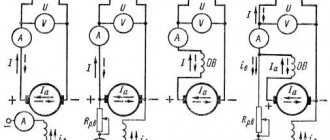
A vacuum diode is a device that works by controlling the heating intensity of the positive and negative poles of the device. When an electric current is applied, the input of the device heats up, after which the effect of electrons leaving the metal appears. If an electric current with a negative voltage is applied, the reverse process of thermionic emission occurs. Due to this, the power that is supplied to the radio component is rectified.
Vah of a semiconductor device
Current-voltage characteristic of a vacuum diode
This characteristic consists of the classic three steps:
- Nonlinear part. The volt-ampere characteristic of the diode at the point of current supply increases at a small rate. This is explained by the effect of counteracting the anode field by the negative voltage of free electrons. In this area, the anode current is extremely low. The effect of stress on force is exponential.
- The second part of the curve is described by the law of power 3/2. The effect of electricity on the anode from the applied voltage in this case is written by the three-second formula, in which the voltage at the anode is multiplied by a constant, the characteristics of the electrode dimensions.
- Saturation voltage. If the anode voltage continues to increase in proportion to previous values, the rate of increase in output current decreases. It is impossible to increase the output power due to the lack of free electrons.
Back-to-back, parallel, series connection of zener diodes
To increase the stabilization voltage, two or more zener diodes can be connected in series. For example, you need to get 17 V at the load, then, if the required rating is not available, support diodes of 5.1 V and 12 V are used.
Parallel connection is used to increase current and power.
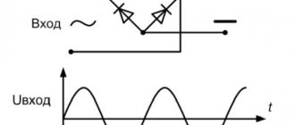
Zener diodes are also used to stabilize alternating voltage. In this case, they are connected in series and counter.
During one half-cycle of alternating voltage, one zener diode operates, and the second operates like a regular diode. In the second half-cycle, semiconductor elements perform opposite functions. However, in this case, the shape of the output voltage will be different from the input voltage and will look like a trapezoid. Due to the fact that the reference diode will cut off a voltage exceeding the stabilization level, the tops of the sine wave will be cut off.
How does a diode work?
Diode Polarity
A diode is a semiconductor device that has one-way conductivity. This characteristic appears due to the characteristics of the pn junction and the resistance at its ends. One-way conductivity means that the radio component will pass electric current only if there is a higher potential at the anode (input). If the power is higher at the cathode, reverse current appears. However, due to the high degree of resistance, the magnitude of such electric current is critically small. In this way, the current-voltage characteristic of the semiconductor device is constructed.
Parasitic properties of the diode:
Temperature influence:
Since drift processes in a semiconductor play an important role, temperature can significantly change the current-voltage characteristics of the pn junction and, accordingly, the parameters of the diode.
Figure 3 - Effect of temperature on the diode's current-voltage characteristic.
Where:
— normal ambient temperature ();
— operating temperature of the diode.
Operating principle of a vacuum type diode
What is a diode - operating principle and device
When electricity is applied to the output of a vacuum diode, electrons leave the surface due to thermionic emission effect. Moreover, with the accumulation of free charged particles in the atmosphere, an area appears that is characterized by a negative potential. A characteristic feature of the vacuum device is that at this time the anode surfaces will begin to be positively charged. Because of this, subsequent charged particles will require a higher level of charge to break away. As a result of transient processes, a cloud of charged particles is formed around the cathode.
Interesting. A small part of the electrons is returned to the output of the radio component. At a temperature that corresponds to the required one and the cloud is stabilized, the output and return of charged particles from the cathode are equalized, which ensures stable movement of charged particles.
List of main characteristics
Below is a table describing the main parameters of rectifier diodes. These characteristics can be obtained from the datasheet (technical description of the element). As a rule, most radio amateurs turn to this information in cases where the element indicated in the diagram is not available, which requires finding a suitable analogue for it.
Table of main characteristics of rectifier diodes
Note that in most cases, if you need to find an analogue of a particular diode, the first five parameters from the table will be quite sufficient. In this case, it is advisable to take into account the operating temperature range of the element and frequency.
Electric current in a vacuum
Current density - what is it and how is it measured?
To make it possible to transmit current in a vacuum, it is necessary to add free charged particles into space using emission phenomena:
- Thermionic - is the process of releasing charged particles by metals during heating. The speed of the process depends on the area, heating conditions and material properties. When kinetic energy exceeds the strength of electronic bonds, particles are released;
- Photoelectronic - occurs under the influence of lighting.
- Field emission occurs due to the influence of the electric field.
Electrical breakdown:
Electrical breakdown occurs due to a sharp increase in reverse current due to a sharp decrease in the resistance of the barrier layer.
An attentive reader will immediately object: “how can this be? After all, an increase in the reverse voltage for a pn junction causes an increase in the geometric dimensions of the blocking layer, and, consequently, its resistance!” And this matter is explained quite simply. Reality always comes up with some difficulties for us, so in semiconductors there are two phenomena - avalanche charge multiplication and the tunnel effect, by name, which divide electrical breakdown into avalanche and tunnel. And if to understand the first effect it is enough to read about its essence, then the tunnel effect is a quantum effect, and to understand it you simply need to strain your brain. Avalanche charge multiplication occurs due to the phenomenon of impact ionization, the essence of which is that electrons, accelerated by an electric field, acquire energy sufficient to knock electrons out of the atoms of the semiconductor crystal lattice, which in turn are also accelerated by this field, and the so-called “avalanche” process of electron separation from atoms by an electric field. The result of these processes is a sharp increase in conductivity, and, consequently, a decrease in the resistance of the barrier layer with virtually no change in its geometric dimensions.
The tunnel effect (also known as the Zener effect in English literature) is most likely in pn junctions of small thickness. Its essence is that electrons having a total energy less than the height of the energy barrier still penetrate through this energy barrier, in our case the barrier of the pn junction, without changing energy, at such voltages when the conduction band in the n-region has equal energy levels with a p-region valence band. This effect is completely quantum and contradicts classical mechanics. As a simplified explanation, we can say the following. From the solution of the Schrödinger equation for the problem of a potential barrier, it follows that the barrier transparency coefficient is non-zero for particles with an energy equal to or less than the height of this barrier. Well, in order to eliminate possible logical difficulties, we can recall the uncertainty relation (Heisenberg relation), which says that if we reduce the uncertainty in the coordinate of a particle, then we increase the uncertainty in the momentum, and vice versa. Consequently, We cannot say with certainty that the particle that passed the barrier actually had a certain energy at the moment of passage.
It should also be noted that the tunnel effect is probabilistic in nature, so the highest probability of its occurrence is in pn junctions with a high concentration of impurities.
Diode Forward and Reverse Voltage
The level of power at which an appliance is open and electricity flows through it is called current. Reverse voltage is negative power that flows from the cathode to the anode. In the case of forward voltage, the level of obstruction to the movement of charged particles is not higher than 100 Ohms, but with reverse voltage the level of resistance increases several hundred times and can reach millions of Ohms.
Diode Forward and Reverse Voltage
Zener diode or Zener diode
The simplest voltage stabilizer in electronics is a zener diode radio element. Sometimes it is also called a Zener diode. In the diagrams, zener diodes are designated something like this:
The terminal with the “cap” is called the same as the diode - cathode, and the other terminal is the anode.
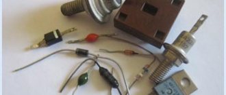
Zener diodes look the same as diodes. In the photo below, on the left is a popular type of modern zener diode, and on the right is one of the samples from the Soviet Union
If you take a closer look at the Soviet zener diode, you can see this schematic designation on it itself, indicating where its cathode is and where its anode is.
I-V characteristics and rectifier diode
The diode's current-voltage characteristic consists of several quadrants:
- In the first case, the device has high conductivity, which corresponds to the applied voltage;
- In the second part, the radio-electronic device receives current until it saturates, then resets;
- In the subsequent segment there is a reverse branch of the diode’s current-voltage characteristic. The approximation of this state indicates low conductivity.
I-V characteristics of the zener diode
Main characteristics of a zener diode
To select a Zener diode for existing purposes, you need to know several important parameters. These characteristics will determine the suitability of the selected device for solving the assigned tasks.
Rated stabilization voltage
The first zener parameter that you need to pay attention to when choosing is the stabilization voltage, determined by the point at which the avalanche breakdown begins. This is where the choice of device to use in the circuit begins. For different instances of ordinary zener diodes, even of the same type, the voltage has a spread of around several percent; for precision ones, the difference is lower. If the nominal voltage is unknown, it can be determined by constructing a simple circuit. You should prepare:
- ballast resistor 1…3 kOhm;
- adjustable voltage source;
- voltmeter (you can use a tester).
It is necessary to increase the voltage of the power source from zero, monitoring the increase in voltage on the zener diode using a voltmeter. At some point it will stop, despite further increasing the input voltage. This is the actual stabilization voltage. If there is no regulated source, you can use a power supply with a constant output voltage obviously higher than Ustabilization. The measurement scheme and principle remain the same. But there is a risk of the semiconductor device failing due to exceeding the operating current.
Zener diodes are used to work with voltages from 2...3 V to 200 V. To generate a stable voltage below this range, other devices are used - stabistors, operating in the direct section of the current-voltage characteristic.
Operating current range
The current at which the zener diodes perform their function is limited above and below. From below it is limited by the beginning of the linear section of the reverse branch of the current-voltage characteristic. At lower currents, the characteristic does not provide a constant voltage mode.
The upper value is limited by the maximum dissipation power that the semiconductor device is capable of and depends on its design. Zener diodes in a metal case are designed for higher current, but do not forget about the use of radiators. Without them, the maximum permissible power dissipation will be significantly less.
It will be interesting➡ Operating principle of a constant voltage generator
Differential resistance
Another parameter that determines the operation of the zener diode is the differential resistance Rst. It is defined as the ratio of the voltage change ΔU to the current change ΔI that caused it. This quantity has the dimension of resistance and is measured in ohms. Graphically, this is the tangent of the angle of inclination of the working section of the characteristic. Obviously, the lower the resistance, the better the quality of stabilization. For an ideal (which does not exist in practice) zener diode Rst is equal to zero - any increase in current will not cause any change in voltage, and the section of the current-voltage characteristic will be parallel to the ordinate axis.
What does the marking mean?
Typical markings:
- The first symbol is D – diode;
- The second is numbering, which corresponds to the type of element, material and method of application;
- The third is the type of device.
The volt-ampere characteristic of a diode shows the main parameters of the diode. Using the graph, you can obtain accurate information about the dependence of the voltage value at the diode output on the input voltage. There are several types of diodes: ideal and real, rectifier and zener diode, silicon and germanium, as well as LED and vacuum. The differences between them are in the work performed. In this case, the formula for the output voltage in the circuit will differ slightly. Since laboratory conditions are rare, minor errors may occur during startup and subsequent operation of the device. The current-voltage characteristic of a semiconductor assembly varies significantly from type to type, different characteristics can be significant.
Types of devices, their designation
By design, there are two types of devices: point and planar. In industry, the most common are silicon (designation: Si) and germanium (designation: Ge). The former have a higher operating temperature. The advantage of the latter is the low voltage drop with forward current.
The designation principle for diodes is an alphanumeric code:
- The first element is the designation of the material from which it is made,
- The second defines a subclass,
- The third denotes working capabilities,
- The fourth is the development serial number,
- Fifth – designation of sorting according to parameters.