Hello dear readers of the site. In the first part of the article, we figured out what a semiconductor is and how current arises in it. Today we will continue the topic we started and talk about the operating principle of semiconductor diodes .
Diode
is a semiconductor device with one
p-n
junction, which has two terminals (anode and cathode), and is designed for rectification, detection, stabilization, modulation, limitation and conversion of electrical signals.
According to their functional purpose, diodes are divided into rectifier, universal, pulse, microwave diodes, zener diodes, varicaps, switching, tunnel diodes, etc.
Theoretically, we know that a diode passes current in one direction and not in the other. But how and in what way he does this is not known and understood by many.
Schematically, a diode can be represented as a crystal consisting of two semiconductors (regions). One region of the crystal has conductivity p
-type, and the other with
n
-type conductivity.
There are holes in the picture
electrons that predominate in the
p
-type region are conventionally depicted as red circles, and
electrons
that predominate in
the n
-type region are shown in blue.
These two areas are the diode's electrodes anode
and
cathode
:
Anode - positive electrode
diode in which the main charge carriers are
holes
.
Cathode - negative electrode
diode in which the main charge carriers are
electrons
.
Contact contacts are applied to the outer surfaces of the areas.
metal layers to which the wire
leads
of the diode electrodes are soldered. Such a device can only be in one of two states:
1. Open
– when it conducts current well;
2. Closed
- when it conducts current poorly.
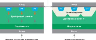
Direct connection of the diode. Direct current.
If you connect a constant voltage source to the diode electrodes: to the anode terminal “ plus
" and the cathode terminal is "
minus
", then the diode will be in
the open
state and a current will flow through it, the magnitude of which will depend on the applied voltage and the properties of the diode.
With this polarity of connection, electrons from the region n
-type electrons will move towards the holes into the
p
-type region, and holes from the
p
-type region will move towards the electrons into the
n
-type region.
At the interface between the regions, called an electron-hole or pn junction , they will meet, where their mutual absorption or recombination
.
For example. Major charge carriers in the n
-type electrons, overcoming
the p-n
junction, enter the
p
-type hole region, in which they become
minority
.
Having become minority electrons, they will be absorbed by majority
carriers in the hole region -
holes
.
In the same way, holes entering the n
-type electronic region become
minority
charge carriers in this region, and will also be absorbed by
the majority
carriers -
electrons
.
Diode pin connected to negative
The pole of a constant voltage source will
give up
n
region , replenishing the decrease in electrons in this region.
And the contact connected to the positive
pole of the voltage source is able
to accept
the same number of electrons
from the
p p
-type region is restored.
Thus, the conductivity the p-n
junction will become
large
and the current resistance will be
small
, which means that a current will flow through the diode, called
diode current Ipr
.
Classification of LEDs by their field of application
Such elements can be indicator and lighting. The former were invented before the latter, and they have long been used in radio electronics. But with the advent of the first lighting LED, a real breakthrough in electrical engineering began. The demand for lighting devices of this type is steadily growing. But progress does not stand still - new types are being invented and put into production, which become brighter without consuming more energy. Let's look in more detail at what LEDs are.
Indicator LEDs: a little history
The first such red LED was created in the middle of the twentieth century. Although it had low energy efficiency and emitted a dim glow, the direction turned out to be promising and developments in this area continued. In the 70s, green and yellow elements appeared, and work to improve them did not stop. By the year 90, the strength of their luminous flux reaches 1 Lumen.
Nowadays, LED lamps can even be like this
The year 1993 was marked by the appearance in Japan of the first blue LED, which was much brighter than its predecessors. This meant that now, by combining three colors (which make up all the shades of the rainbow), you can get any color. In the early 2000s, the luminous flux already reached 100 Lumens. Nowadays, LEDs continue to improve, increasing brightness without increasing power consumption.
Use of LEDs in household and industrial lighting
Now such elements are used in all industries, be it machine or automotive manufacturing, lighting of production workshops, streets or apartments. If we take the latest developments, we can say that even the characteristics of LEDs for flashlights are sometimes not inferior to old 220 V halogen lamps. Let's try to give one example. If we take the characteristics of a 3 W LED, they will be comparable to the data of an incandescent lamp with a consumption of 20-25 W. The result is energy savings of almost 10 times, which, with daily constant use in an apartment, provides a very significant benefit.
LED flashlights with special lenses shine at a distance of up to 3 km
What are the benefits of LEDs and are there any disadvantages to them?
A lot can be said about the positive qualities of light diodes. The main ones include:
- Cost-effectiveness without loss of luminous flux power - here they are unrivaled;
- Durable housing – there is no danger of mechanical damage;
- Durability - such elements work tens of times longer than incandescent lamps;
- Compactness – have small dimensions;
- The safest - they operate from a 3-24 V network;
- Eco-friendly - do not require special disposal.
As for the negative aspects, there are only two of them:
- Work only with constant voltage;
- It follows from the first - the high cost of lamps based on them due to the need to use a driver (electronic stabilizing unit).
Ultraviolet and infrared light diodes - they even make such
Reverse connection of the diode. Reverse current.
Let's change the polarity of the constant voltage source - the diode will be closed
condition.
In this case, electrons in the region n
-type will move towards
the positive
pole of the power source, moving away from
the p-n
junction, and holes in the
p
-type region will also move away from
the p-n
junction, moving towards
the negative
pole of the power source.
As a result, the boundary of the regions will seem to expand, which creates a zone depleted of holes and electrons, which will provide great
resistance to the current.
But, since in each of the regions of the diode there are minor
charge carriers, then a small exchange of electrons and holes between the regions will still occur.
Therefore, a current many times less than the forward current will flow through the diode, and such a current is called the reverse current of the diode ( Irev
).
As a rule, in practice, the reverse current p-n
junction is neglected, and from this we conclude that
the p-n
junction has only
one-way conductivity
.
Lumen
As you already understand, candelas are not suitable for assessing the luminous intensity of high-power LEDs. lumens for this - this is the total amount of light that an LED can produce when connected with given current and voltage values. Remember the fire bucket analogy? It fits here too. Let's assume that if the LED has a light intensity of 100 lumens, then there will be 100 lumens in our bucket. An ordinary 100 W light bulb is also a Lambertian source. The average light output of this bulb is 10-15 lumens per watt. That is, 100 watts of incandescent lamp will give us, say, 1000 lumens. This means that to replace a 100 W lamp with LEDs, you need 10 pieces of 100 lumens. Is it that simple? No Unfortunately. We come to such a term as LUX.
Forward and reverse diode voltage.
The voltage at which the diode opens and direct current flows through it is called forward
(Upr), and the voltage of reverse polarity, at which the diode closes and reverse current flows through it, is called
reverse
(Urev).
At forward voltage ( Upr
) the resistance of the diode does not exceed several tens of ohms, but with reverse voltage (
Urev
) the resistance increases to several tens, hundreds and even thousands of kiloohms. This is not difficult to verify if you measure the reverse resistance of the diode with an ohmmeter.
Resistance pn
diode transition value is not constant and depends on the forward voltage (
Upr
), which is supplied to the diode.
The greater
this voltage, the
less
the p-n
has , the
greater
the forward current
Ipr
flows through the diode.
In the closed state drops
, therefore, the reverse current passing through it
is small
, and the resistance of
the p-n
junction
is high
.
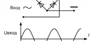
For example. If you connect a diode to an alternating current circuit, it will open at positive
half-cycles at the anode, freely passing
forward current
(Ipr), and close at
negative
half-cycles at the anode, almost without passing current in the opposite direction -
reverse current
(Irev).
These properties of diodes are used to convert alternating current into direct current
, and such diodes are called
rectifying
.
Current-voltage characteristic of a semiconductor diode.
Dependence of the current passing through pn
the transition, depending on the magnitude and polarity of the voltage applied to it, is depicted in the form of a curve called
the current-voltage characteristic of the diode .
The graph below shows such a curve. Vertical _
The axis in the upper part indicates the values of the forward current (
Ipr
), and in the lower part - the reverse current (
Irev
).
Along the horizontal
axis on the right side the values of the forward voltage
Upr
, and on the left side the values of the reverse voltage (
Urev
) are indicated.
The current-voltage characteristic consists of two branches: direct branch
, in the upper right part, corresponds to the forward (pass) current through the diode, and
the reverse branch
, in the lower left part, corresponding to the reverse (closed) current through the diode.
Direct branch
goes steeply upward, pressing against
the vertical
axis, and characterizes the rapid increase in forward current through the diode with increasing forward voltage.
The reverse branch
runs almost parallel to
the horizontal
axis and characterizes a slow increase in the reverse current.
The steeper the forward branch is to the vertical axis and the closer the reverse branch is to the horizontal, the better the rectifying properties of the diode. The presence of a small reverse current is a disadvantage of diodes
.
From the current-voltage characteristic curve it is clear that the forward current of the diode ( Ipr
) is hundreds of times greater than the reverse current (
Irev
).
As the forward voltage increases through pn
The transition current initially increases slowly, and then a section of rapid current growth begins.
This is explained by the fact that a germanium
diode opens and begins to conduct current at a forward voltage of 0.1 - 0.2V, and
a silicon diode
at 0.5 - 0.6V.
For example. At forward voltage Upr
= 0.5V forward current
Ipr
is equal to 50mA (point “
a
” on the graph), and already at a voltage
Upr
= 1V the current increases to 150mA (point “
b
” on the graph).
But such an increase in current leads to heating of the semiconductor molecule. And if the amount of heat generated is greater than that removed from the crystal naturally, or using special cooling devices ( radiators
), then irreversible changes can occur in the conductor molecule, up to the destruction of the crystal lattice.
Therefore, the forward current the p-n
junction is limited to a level that prevents overheating of the semiconductor structure. To do this, use a limiting resistor connected in series with the diode.
For semiconductor diodes, the forward voltage Upr is
at all values of operating currents does not exceed: for
germanium
- 1V;
for silicon
- 1.5V.
With an increase in reverse voltage ( Urev
) applied to
the pn
junction, the current increases slightly, as evidenced by the reverse branch of the current-voltage characteristic.
For example. Let's take a diode with the parameters: Urev max
= 100V,
Irev max
= 0.5 mA, where:
Uar max
– maximum constant reverse voltage, V;
Irev max
– maximum reverse current, µA.
With a gradual increase in the reverse voltage to a value of 100V, one can see how the reverse current increases slightly (point “ at
" on the chart).
But with a further increase in voltage, above the maximum for which the pn
breakdown
occurs .
LED device.
An LED diode consists of a semiconductor crystal, which is mounted on a substrate, a housing with contacts, and an optical system.
The devices of indicator (DIP), flat (SMD) and SOV elements differ externally.
DIP design device.
Sectional view of a DIP LED.
Contacts are mounted at the base of the device. A crystal (one or more) is fixed to the cathode. A wire is attached to the crystal. It connects the semiconductors to the anode. This is necessary for grouping two conductors with different types of conductivity. The LED element is hermetically covered with a lens on top. The device body is made in the form of an epoxy resin cylinder, the edge of which is cut off from the cathode side. The LED element is mounted by soldering long leads.
SMD design device.
Sectional view of an SMD LED.
The body is made of a parallelepiped. Its basis is a heat sink from the crystal. A semiconductor element is mounted on it. A contact wire connects it to the anode. The contacts are made flat. The element is hermetically covered with a lens on top.
Structural device of SOV.
COB technology is the latest direction in production.
Such light-emitting diodes have a thermally conductive substrate (usually aluminum) at the base. Semiconductor crystals, which are connected in a series-parallel circuit, are attached to it with non-conductive glue. Everything is covered with phosphor on top.
This type of LED is easy to install, produces a good luminous flux and does not distort colors. They are in demand in the production of small, bright spotlights and decorative lighting. Unlike DIP and SMD, they are capable of operating at elevated temperatures. But due to their design, they have a shorter service life in comparison.
If many crystals are mounted on one substrate, then such an LED element is called an LED matrix.
PCB Star design device.
It consists of one large crystal, which is mounted on an aluminum substrate in the shape of a star. Due to the increased crystal area, the LED power increases. Makes it easier to focus. Therefore, PCB Star is in demand in the production of bright light sources: from flashlights to floodlights.
Electrical breakdown.
Electrical breakdown occurs as a result of exposure to a strong electric field
in
p-n
junction.
Such a breakdown is reversible
, that is, it does not damage the junction, and when the reverse voltage is reduced, the properties of the diode are preserved.
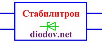
For example. Zener diodes
- diodes designed to stabilize voltage - operate in this mode
Tunnel breakdown.
Tunnel breakdown occurs as a result of the phenomenon of the tunnel effect
, which manifests itself in the fact that with a strong electric field strength acting in
p-n
junction
of small thickness
, some electrons penetrate (leak) through the transition from the
p
the n
region without
changing
their energy.
Thin p-n
junctions are possible only with a high concentration
of impurities
in the semiconductor molecule.
Depending on the power and purpose of the diode, the thickness of the electron-hole junction can range from 100 nm
(nanometers) to
1 micron
(micrometer).
A tunnel breakdown is characterized by a sharp increase in reverse current
with a slight
reverse voltage
- usually a few volts.
Tunnel diodes
operate based on this effect .
Due to their properties, tunnel diodes are used in amplifiers, generators of sinusoidal relaxation oscillations and switching devices at frequencies of up to hundreds and thousands of megahertz.
Avalanche breakdown.
Avalanche breakdown is that, under the influence of a strong electric field, minority
Charge carriers under the influence of
heat
in
a pn
junction are accelerated so much that they are able to
knock out
one of its valence electrons from an atom and
throw
it into the conduction band, thereby forming an
electron-hole
.
The resulting charge carriers will also begin to accelerate and collide with other atoms, forming the following electron-hole pairs. The process takes on an avalanche-like character, which leads to a sharp increase
in reverse current at a practically
constant
voltage.
Diodes that use the avalanche breakdown effect are used in powerful rectifier units
, used in the metallurgical and chemical industries, railway transport and other electrical products in which a reverse voltage higher than permissible may occur.
What are SMD LEDs: their characteristics and differences from conventional ones
A clear decoding of this abbreviation looks like Surface Mount Devices, which literally means “surface mounted”. To make it clearer, we can recall that ordinary cylindrical light diodes on legs are recessed into the board and soldered on the other side. In contrast, SMD components are fixed with claws on the same side where they themselves are located. This installation makes it possible to create double-sided printed circuit boards.
Such LEDs are much brighter and more compact than conventional ones and are elements of a new generation. Their dimensions are indicated in the marking. But do not confuse the size of the SMD LED and the crystal (chip) of which there can be many in the component. Let's look at several of these light diodes.
Here they are, LED SMD2835. Small, but there is enough light from them
LED SMD2835 parameters: dimensions and characteristics
Many novice craftsmen confuse the markings SMD2835 with SMD3528. On the one hand, they should be the same, because the marking indicates that these LEDs have sizes of 2.8x3.5 mm and 3.5 by 2.8 mm, which are the same thing. However, this is a misconception. The technical characteristics of the SMD2835 LED are much higher, while it has a thickness of only 0.7 mm versus 2 mm for the SMD3528. Let's look at the SMD2835 data with different powers:
| Parameter | Chinese 2835 | 2835 0.2W | 2835 0.5W | 2835 1W |
| Luminous flux strength, Lm | 8 | 20 | 50 | 100 |
| Power consumption, W | 0,09 | 0,2 | 0,5 | 1 |
| Temperature, in degrees C | +60 | +80 | +80 | +110 |
| Current consumption, mA | 25 | 60 | 150 | 300 |
| Voltage, V | 3,2 |
As you can understand, the technical characteristics of SMD2835 can be quite varied. It all depends on the quantity and quality of crystals.
5050 LED Specifications: Larger SMD Component
It is quite surprising that, despite its large dimensions, this LED has a lower luminous flux than the previous version - only 18-20 Lm. The reason for this is the small number of crystals - usually there are only two. The most common application of such elements is in LED strips. The density of the strip is usually 60 pcs/m, which gives a total of about 900 lm/m. Their advantage in this case is that the tape gives a uniform, calm light. In this case, the angle of its illumination is maximum and equal to 120.
A “corn” lamp is made using such elements
Such elements are produced with a white glow (cold or warm shade), single-color (red, blue or green), three-color (RGB), as well as four-color (RGBW).
Characteristics of SMD5730 LEDs
Compared to this component, the previous ones are already considered obsolete. They can already be called super bright LEDs. 3 volts, which feed both 5050 and 2835, produce here up to 50 lm at 0.5 watts. The technical characteristics of the SMD5730 are an order of magnitude higher, which means they need to be considered.
| Parameter | Index |
| Luminous flux strength, Lm | 45-50 |
| Power consumption, W | 0,5 |
| Operating temperature range, degrees C | -40 to +80 |
| Rated current, mA | 150 |
| Operating voltage, V | 3,1-3,2 |
| Illumination Angle | 120 degrees |
Still, this is not the brightest LED of SMD components. Relatively recently, elements appeared on the Russian market that literally outshone all others. We will talk about them now.
Cree LEDs: characteristics and technical data
To date, there are no analogues to Cree products. The characteristics of their super bright LEDs are truly amazing. If previous elements could boast a luminous flux of only 50 Lm from one chip, then, for example, the characteristics of the XHP35 LED from Cree speak of 1300-1500 Lm from one chip. But their power is also greater - it is 13 W.
If we summarize the characteristics of various modifications and models of LEDs of this brand, we can see the following:
| Modification | XM-L | XR-E, XP-G, XP-E, XP-C | ||||||
| Luminous flux intensity, Lm/W | T5 (260 to 280) | T6 (280 to 300) | U2 (300 to 320) | Q2 (87.4 to 93.9) | Q3 (from 93.9 to 100) | Q4 (100 to 107) | Q5 (107 to 114) | R2 (114 to 122) |
The luminous flux strength of SMD LED “Cree” is called a bin, which is mandatory to be marked on the packaging. Recently, a lot of counterfeits of this brand have appeared, mostly made in China. When purchasing, it is difficult to distinguish them, but after a month of use, their light dims and they cease to differ from others. At a fairly high cost, such an acquisition will be a rather unpleasant surprise.
The filament is gradually fading into history
We offer you a short video on this topic: