I-V characteristic of the diode:
First, let's look at the current-voltage characteristic of an ideal diode.
Figure 1 - I-V characteristic of an ideal diode.
As can be seen from the graph, the diode conducts current only when there is a forward voltage at its terminals (i.e., plus at the anode, minus at the cathode). Current I 0 is the saturation current, i.e. The maximum reverse current caused by the thermal drift of current carriers in the region of the pn junction is several orders of magnitude less than the forward current.
For fans of formulas, it can be noted that the current-voltage characteristic of an ideal diode is described by the following expression:
Spoiler
Where:
I 0 – saturation current.
— thermal potential (e is the elementary charge of the electron, k is Boltzmann’s constant, T is the absolute temperature).
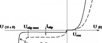
However, in life, as you know, not everything is so simple and you have to constantly strain your brain. The current-voltage characteristic of a real diode is somewhat different.
Figure 2 - I-V characteristic of a real diode.
The first difference is the different diode opening voltage ( U0 ), depending on the semiconductor material used . For silicon ( Si ) it is approximately 0.7 V ; for germanium ( Ge ) – 0.3 V.
The second difference is a different type of reverse branch, the presence of a breakdown of the pn junction.
Usually, areas of electrical (A-B) and thermal (B-C) breakdown are distinguished. Electrical breakdown inherently violates only the electrical insulation of pn junction regions, so it is reversible. Thermal breakdown, on the contrary, violates the physical integrity of the pn junction; in fact, it simply burns out; it is obvious that thermal breakdown is irreversible and renders the element unusable.
If you are interested in the reasons for the breakdown, then the next paragraph is for you.
Spoiler
Avalanche Diode Optimization
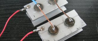
Rice. No. 1. Powerful power avalanche diode DL153-2000, appearance.
Powerful avalanche diodes of the DL153-2000 are used in three-phase converters, the frequency of which reaches 500 Hz; they are used to rectify the voltage of powerful turbogenerators with a power of up to 320 MW. To reduce operating temperatures (permissible value 175°C) in long-term (nominal) mode and boost mode at a frequency of 500 Hz, it is necessary to take certain measures. A decrease in the operating life of the converter and an exponential (proportional to the value of the growth rate) increase in the failure rate due to an increase in the temperature of the silicon structure.
Rice. No. 2. Drawing of a power avalanche diode DL153-2000.
The research program to reduce power losses and lower temperatures includes the following studies:
- Use of radiation defects for doping the silicon structure of a diode.
- Measuring the lifetime of charge carriers using the Lax method;
- Monitoring the parameters of statics and dynamics of diodes.
- Finding the total power losses and temperature values of the diode structure with an attached cooler.
The result of an optimization study, using irradiation of the silicon structure of a semiconductor device with accelerated electrons, showed an improvement in the system of parameters. The total power losses decreased in all operating modes by 37%, and the temperature was reduced by 28%. The result confirmed the effectiveness of structure irradiation for obtaining reliable power semiconductor devices.
Avalanche diode
Rice. No. 3. Structure of an avalanche-transit diode.
A type of avalanche diode is an avalanche-transit diode (IMPATT diode). It is built on the basis of avalanche multiplication of charged carriers. The device is used to generate oscillations in the microwave range. The working area of the device is the area of avalanche breakdown.
The structure consists of silicon and gallium arsenide (metal semiconductor) and others. In the base of the diode, a region filled with electrons and holes with a constant current value, a phase appears that is characterized by a high field strength; it precedes the appearance of an avalanche shock front.
The main mode of the avalanche-transit diode is the trapped plasma mode, the state of compensated semiconductor plasma. There is a separate type of such diodes - BARITT diodes, they are characterized by injection-flight mode.
Process Quality Indicators for Avalanche Diode Design
The main advantage of an avalanche diode over a rectifier is its ability to restore parameters as a result of large overvoltages, while the latter are destroyed and fail.
Rice. No. 4. Drawing with overall and connecting dimensions of an avalanche diode of type: a) DL152 and b) DP151.
Design quality requirements include:
- During the manufacturing process of diodes, the dislocation density of large diameter silicon above 60 mm is limited to 102 cm2.
- Swirl defects are excluded.
- The content of O2 and C in silicon is limited, which is converted into complex Si-O and Si-C complexes.
- The impurity atmosphere of heavy and alkali metal impurities on dislocations is significantly reduced.
- Existing so-called “star defects”, in the form of microcracks that appear as a result of heat treatment in stressed silicon and deteriorate the current-voltage characteristics of the device, are significantly reduced.
Rice. No. 5. Parameters of some types of avalanche diodes.
Avalanche breakdown
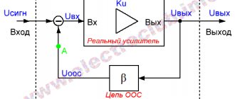
Although the diode behaves as an insulator when reverse biased, further increasing the applied voltage results in a situation where the junction suddenly begins to conduct (Figure 1.12). This happens due to electrons of thermal origin, which, due to the electric field in the depletion layer, acquire energy sufficient to form new electron-hole pairs upon collision with silicon atoms. These newly formed carriers then create free carriers themselves, and the avalanche grows. The process does not lead to destruction of the junction if the current is limited and thereby prevented from overheating. can occur at voltages from 5 to 1000 V and higher. The breakdown voltage depends on the design of the diode and the degree of doping of the silicon. The value of the breakdown voltage limits the reverse peak voltage in the rectifiers.
Special diodes with low breakdown voltage are produced, which are called Zener diodes, named after Karl Zener, who discovered the mechanism of electrical breakdown in 1934. Zener diodes (zener diodes. - Note transl.)
usually have a very high degree of doping, creating a high concentration of majority carriers and allowing the depletion layer to remain thin even when the junction is reverse biased. As a result, the potential gradient becomes so large that breakdown can occur at a reverse voltage of less than 3 V. The very steep breakdown characteristic shown in Fig. 1.12, suggests that the voltage drop across the diode in breakdown mode remains almost constant when the reverse current changes over a wide range. Therefore, zener diodes are used to stabilize the output voltage in power supplies (see Chapter 9). Strictly speaking, the concept of Zener breakdown includes a tunnel effect when overcoming a potential barrier and is applicable only to diodes with a breakdown voltage of less than 5 V, and with a breakdown voltage of more than 5 V, diodes are more correctly called avalanche.
Rice. 1.12. Characteristics of a reverse-mixed diode with typical avalanche breakdown.
Transition capacitance and varicaps
A reverse-biased diode behaves like a small capacitor, with a typical capacitance value of 2 pF for a low-power silicon diode. The depletion layer behaves as a dielectric insulator between the conducting “plates” “- and p-
type. Additionally, as the bias voltage increases, the capacitance drops slightly as the depletion layer expands. By appropriate doping, special diodes are created - varicaps, for which a typical change in capacitance is from 10 to 2 pF with an increase in reverse voltage from 2 to 30 V. Such diodes are widely used when tuning radios and televisions in the meter and decimeter wavelength range. The device for electronically controlling the capacitance of the tuning capacitor is often a special circuit (automatic frequency control circuit) that locks the tuning to the desired station automatically.
Literature: M.H. Jones, Electronics - practical course Moscow: Tekhnosphere, 2006. - 512 p. ISBN 5-94836-086-5
Tweet Like
- Previous post: Logic functions and logic circuits
- Next post: Velleman Virtual Function Generators
- POWER SUPPLY FOR CAR RADIO (0)
- BATTERY CHARGER (0)
- LITHIUM-NON CELL CHARGER CHARGER CONTROLLER (0)
- BATTERY CHARGING CURRENT LIMITER (0)
- BATTERY VOLTAGE INDICATOR SIMPLE CIRCUIT (0)
- BATTERY VOLTAGE LEVEL INDICATOR (0)
- BATTERY CHARGING MODE INDICATOR (0)