What is the difference between forward and reverse bias?
Applying a voltage to a diode such that the diode begins to pass current is called forward bias. Applying a voltage to a diode such that the diode stops passing current is called reverse biasing.
Interesting materials:
How to recover photos? How to restore WhatsApp function? How to restore gallery on Android? How to restore gallery on Samsung Android? How to restore gallery on Android? How to restore gallery on Samsung? How to restore a gallery on a smartphone? How to recover MBR Master Boot Record? How to recover a voice message on WhatsApp? How to restore government services if there is no number?
Direct diode connection
The pn junction of the diode can be affected by voltage supplied from external sources. Indicators such as magnitude and polarity will affect its behavior and the electrical current conducted through it.
Below we consider in detail the option in which the positive pole is connected to the p-type region, and the negative pole to the n-type region. In this case, direct switching will occur:
- Under the influence of voltage from an external source, an electric field will be formed in the pn junction, and its direction will be opposite to the internal diffusion field.
- The field voltage will decrease significantly, which will cause a sharp narrowing of the blocking layer.
- Under the influence of these processes, a significant number of electrons will be able to freely move from the p-region to the n-region, as well as in the opposite direction.
- The drift current indicators during this process remain the same, since they directly depend only on the number of minority charged carriers located in the pn junction region.
- Electrons have an increased level of diffusion, which leads to the injection of minority carriers. In other words, in the n-region there will be an increase in the number of holes, and in the p-region an increased concentration of electrons will be recorded.
- The lack of equilibrium and an increased number of minority carriers causes them to go deep into the semiconductor and mix with its structure, which ultimately leads to the destruction of its electrical neutrality properties.
- In this case, the semiconductor
I-V characteristic of a real semiconductor diode
However, in practice, due to its semiconductor structure, a real diode has a number of disadvantages and limitations compared to an ideal diode. This can be seen in the graph below.
Vϒ(gamma) - conductivity threshold voltage
When switched on directly, the voltage across the diode must reach a certain threshold value - Vϒ. This is the voltage at which the PN junction in the semiconductor opens enough for the diode to begin conducting current well. Before the voltage between the anode and cathode reaches this value, the diode is a very poor conductor. Vϒ for silicon devices is approximately 0.7V, for germanium devices - about 0.3V.
ID_MAX - maximum current through the diode when connected directly
When connected directly, the semiconductor diode can withstand a limited current ID_MAX. When the current through the device exceeds this limit, the diode overheats. As a result, the crystal structure of the semiconductor is destroyed, and the device becomes unusable. The magnitude of this current varies greatly depending on the different types of diodes and their manufacturers.
IOP – reverse leakage current
When switched in reverse, the diode is not an absolute insulator and has a finite resistance, albeit a very high one. This causes leakage current or reverse current IOP to form. The leakage current for germanium devices reaches up to 200 µA, for silicon devices up to several tens of nA. The latest high quality silicon diodes with extremely low reverse current are around 0.5 nA.
PIV(Peak Inverse Voltage) - Breakdown voltage
When reverse-connected, the diode can withstand a limited voltage - the breakdown voltage PIV. If the external potential difference exceeds this value, the diode sharply lowers its resistance and turns into a conductor. This effect is undesirable, since the diode should only be a good conductor when connected directly. The breakdown voltage varies depending on the different types of diodes and their manufacturers.
Parasitic capacitance of PN junction
Even if a voltage significantly higher than Vϒ is applied to the diode, it will not immediately begin to conduct current. The reason for this is the parasitic capacitance of the PN junction, which takes some time to fill. This affects the frequency characteristics of the device.
Theoretical part
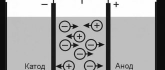
The operation of semiconductor diodes is based on the properties of the pn junction, which is formed at the interface between the semiconductor regions with hole (p) and electronic conductivity (n). The concentration of electrons in the n-region is significantly greater than in the p-region, and there are more holes in the p-region than in the n-region. The unequal density of particles causes the diffusion of majority carriers from areas of higher concentration: electrons from the n - region and holes from the p - region. As a result of recombination, a carrier-depleted layer appears at the boundary of the p- and n-regions, which is called a blocking layer (Fig. 1, a). Ions of donor and acceptor impurities in the region of the blocking layer create an electric field with a strength Evn, which prevents further diffusion of majority carriers and creates a drift current caused by minority carriers.
Figure 1. Semiconductor diode
When connecting an emf source. to the np junction, depending on the direction of the source voltage vector, the width of the blocking layer can:
- Decrease - the voltage vectors of the source and the blocking layer are opposite, which leads to an increase in the diffuse current;
- Increase - the voltage vectors of the source and the blocking layer are directed in the same direction, which leads to a decrease in diffusion currents to almost zero and an increase in the drift current.
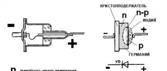
The listed properties of pn junctions are used in semiconductor diodes. Semiconductor diodes have asymmetrical electron-hole junctions. One region of the semiconductor with a higher concentration of impurities (the highly doped region) serves as the emitter, and another with a lower concentration of impurities (the low-doped region) serves as the base.
The terminal that connects the emitter to the external electrical circuit is called cathode, and the terminal that connects to the base is called anode (Fig. 1, b).
Rectifier diodes are designed to convert alternating current into unidirectional current. The volt-ampere characteristic (CVC) of a semiconductor diode is shown in Fig. 2.
Figure 2. I-V characteristics of a semiconductor diode
The volt-ampere characteristic has a direct (“1” in Fig. 2) and a reverse (“2” in Fig. 2) branches. When the diode is turned on in the forward direction (the forward branch of the current-voltage characteristic), the voltage vector of the external source Eist is directed opposite to the voltage vector of the pn junction of the diode, the positive pole of the source is connected to the anode of the diode, and the negative pole to the cathode of the diode. In this case, the total tension vector decreases. This leads to a decrease in the potential barrier in the pn junction.
In this mode, part of the majority charge carriers with the highest energy values will overcome the lowered potential barrier and pass through the pn junction. In the transition, the equilibrium state will be disrupted, and a diffusion current will flow through it due to the injection of electrons from the n-region into the semiconductor and holes from the p-region into the n-semiconductor.
The voltage Uthr, from which small increments of forward voltage cause a sharp increase in current, is called threshold.
When the diode is turned on in the reverse direction (reverse branch of the current-voltage characteristic), the direction of the external source voltage vector Eist coincides with the transition field strength vector: the negative pole of the source is connected to the cathode of the diode, and the positive pole of the source is connected to the anode of the diode. This inclusion of the diode leads to an increase in the potential barrier of the pn junction of the diode and the current through the junction will be determined by minority charge carriers: electrons from the p-region to the n-region and holes from the n-region to the p-region. This process is called minority carrier extraction, and the current flowing through the diode is called reverse current Irev.
With a further increase in the reverse voltage applied to the diode, at a certain value of Urev1, a sharp increase in the reverse current will occur in it - section “3” in Figure 2. This phenomenon is called breakdown. A distinction is made between electrical and thermal breakdown of pn junctions. Avalanche breakdown is an electrical breakdown of a transition caused by an avalanche multiplication of charge carriers under the influence of a strong electric field. Electrons, having accelerated in the field of the blocking layer, knock out valence electrons from the atoms of the semiconductor, which, in turn, manage to accelerate and knock out new electrons, etc. The process develops like an avalanche and is accompanied by a rapid increase in reverse current.
Thermal breakdown occurs due to overheating of the pn junction or a separate section of it (section “4” in Fig. 2). In this case, intensive generation of electron-hole pairs occurs and the reverse current increases, which leads to an increase in the power released in the pn junction and its further heating. This process is also avalanche-like and ends with the melting of the overheated junction section and failure of the diode.
Depending on the ratio of the linear dimensions of the rectifying pn junction, semiconductor diodes are divided into two classes: point and planar. Point diodes have a low pn junction capacitance and are used to rectify alternating current of any frequency up to microwave. In planar diodes, the capacitance of the pn junction is several tens of pF.
Diode operation and its current-voltage characteristics
The current-voltage characteristic of these devices is understood as a curved line that shows the dependence of the electric current flowing through the pn junction on the volume and polarity of the voltage acting on it.
Such a graph can be described as follows:
- The axis is located vertically: the upper area corresponds to the forward current values, the lower area to the reverse current parameters.
- Horizontal axis: The area on the right is for forward voltage values; area on the left for reverse voltage parameters.
- The direct branch of the current-voltage characteristic reflects the passing electric current through the diode. It is directed upward and runs in close proximity to the vertical axis, since it represents the increase in forward electric current that occurs when the corresponding voltage increases.
- The second (reverse) branch corresponds to and displays the state of the closed electric current, which also passes through the device. Its position is such that it runs virtually parallel to the horizontal axis. The steeper this branch approaches the vertical, the higher the rectifying capabilities of a particular diode.
- According to the graph, it can be observed that after an increase in the forward voltage flowing through the pn junction, a slow increase in the electric current occurs. However, gradually, the curve reaches an area in which a jump is noticeable, after which an accelerated increase in its indicators occurs. This is due to the diode opening and conducting current at forward voltage. For devices made of germanium, this occurs at a voltage of 0.1V to 0.2V (maximum value 1V), and for silicon elements a higher value is required from 0.5V to 0.6V (maximum value 1.5V).
- The indicated increase in current readings can lead to overheating of semiconductor molecules. If the heat removal that occurs due to natural processes and the operation of radiators is less than the level of its release, then the structure of the molecules can be destroyed, and this process will be irreversible. For this reason, it is necessary to limit the forward current parameters to prevent overheating of the semiconductor material. To do this, special resistors are added to the circuit, connected in series with the diodes.
- By examining the reverse branch, you can notice that if the reverse voltage applied to the pn junction begins to increase, then the increase in current parameters is virtually unnoticeable. However, in cases where the voltage reaches parameters exceeding the permissible norms, a sudden jump in the reverse current may occur, which will overheat the semiconductor and contribute to the subsequent breakdown of the pn junction.
What is an ideal diode?
The main task of a conventional rectifier diode is to conduct electric current in one direction and not allow it to pass in the opposite direction.
Therefore, an ideal diode should be a very good conductor with zero resistance when the voltage is connected forward (plus to the anode, minus to the cathode), and an absolute insulator with infinite resistance when the voltage is reversed. This is what it looks like on the graph:
This diode model is used in cases where only the logical function of the device is important. For example, in digital electronics.
Diode reverse connection
Now we will consider another method of switching on, during which the polarity of the external source from which the voltage is transmitted changes:
- The main difference from direct connection is that the created electric field will have a direction that completely coincides with the direction of the internal diffusion field. Accordingly, the barrier layer will no longer narrow, but, on the contrary, expand.
- The field located in the pn junction will have an accelerating effect on a number of minority charge carriers, for this reason, the drift current indicators will remain unchanged. It will determine the parameters of the resulting current that passes through the pn junction.
- As the reverse voltage , the electric current flowing through the junction will tend to reach its maximum. It has a special name - saturation current.
- In accordance with the exponential law , with a gradual increase in temperature, the saturation current indicators will also increase.