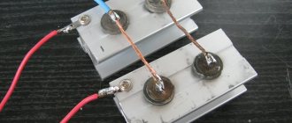
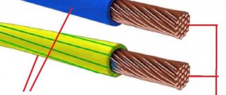
Low-frequency diodes (tablet version)
Diodes D133-400, D133-500, D133-800, D143-630, D143-800, D143-1000, D253-1600 are intended for use in DC and AC circuits with a frequency of up to 500 Hz in general-purpose electrical devices. The diodes are resistant to sinusoidal vibration in the frequency range 1-100 Hz with an acceleration of 49 m/s2 and single shocks lasting 50 ms with an acceleration of 39.2 m/s2. The anode and cathode are flat bases, with polarity identified by the polarity symbol printed on the diode body.
Low-frequency avalanche diodes are designed for use in general-purpose devices with frequencies up to 500 Hz. The diodes allow exposure to vibration loads in the frequency range of 1-100 Hz with an acceleration of 49 m/s2, multiple impacts lasting 2-15 ms with an acceleration of 147 m/s2 and single impacts lasting 50 ms with an acceleration of 39.2 m/s2. Diodes DL 161-200, DL 171-320 have a pin design. The anode of the diodes is a copper base, the cathode is a flexible lead. Diodes DL 123-320, DL133-500 have a tablet design. The anode and cathode are flat bases, with polarity identified by the polarity symbol printed on the diode body.
Circuit of the simplest AC rectifier
Let's look at how the circuit works (the rectifier diode plays the main role in it) of a primitive rectifier.
AC mains voltage with positive and negative half-cycles is supplied to its input. A load (R load) is connected to the output of the rectifier, and the function of the element rectifying the current is performed by a diode (VD).
Positive half-cycles of voltage applied to the anode cause the diode to open. At this time, direct current (I direct) flows through it, and therefore through the load (R load), which is powered by the rectifier.
Negative half-cycles of voltage applied to the anode of the diode cause it to close. A small reverse diode current flows through the circuit (I reverse). Here the diode cuts off the negative half-wave of the alternating current.
As a result, it turns out that a pulsating, rather than an alternating current of one direction, now passes through the load connected to the network (R load), through the diode (VD). After all, it can take place exclusively in positive half-cycles. This is the meaning of AC rectification.
However, such a voltage can only power a low-power load that is powered from an AC mains and does not have serious power requirements, for example, an incandescent lamp.
The lamp will transmit voltage only when positive pulses pass through, as a result of which the electrical appliance is subject to slight flickering with a frequency of 50 Hz. True, due to the fact that the thread is subject to thermal inertia, it will not be able to completely cool down in the intervals between pulses, which means that the flickering will be almost unnoticeable.
If such voltage is applied to an amplifier or power receiver, a low frequency sound (50 Hz) will be heard in the loudspeaker, which is called AC hum. This effect occurs because the pulsating current, when passing through the load, induces a pulsating voltage in it, generating a hum.
This disadvantage is to some extent eliminated if a filter capacitor (C filter), the capacitance of which is quite large, is connected in parallel with the load.
The capacitor will be charged by current pulses during positive half-cycles, and discharged through the load (R load) during negative half-cycles. If the capacitor capacity is sufficient, during the time that passes between two current pulses, it will not have time to completely discharge, and therefore, there will be a constant current on the load (R load).
But even with such a relatively smooth current, the load should not be powered either, because it will continue to generate noise, because the magnitude of the ripples (U puls.) is still quite serious.
Rectifier or power diodes
Rectifier (power) diodes are semiconductor devices designed to convert alternating current into unipolar current. To do this, the diode is connected in series to the circuit of the AC source and load (Figure 24). Rice. 24. Electrical circuit diagram with a rectifying diode
The basis of the diode design is one p-n junction. The diode designation has been preserved from the first vacuum diodes. In the image, the line means the cathode, and the triangle means the anode. To remember this, it is enough to imagine that the cathode emits electrons, and they come out of it in a diverging beam, forming a triangle. If we consider the conductivity of the diode to be directed from plus to minus, then it will correspond to the arrow formed by the vertex of the triangle.
Due to the one-way conductivity of the diode, a pulsating current of one polarity flows through the load (Figure 25).
Rice. 25. Current-voltage characteristic of the diode and graph of current changes on Rн (Fig. 24)
The main parameters of rectifier diodes are:
a) Maximum rectified current Iрmax ;
b) Maximum permissible reverse voltage Urevmax ;
c) Reverse current flowing through the diode Iprmax ;
d) Voltage drop across the diode when connected directly Upp .
Rectifier diodes are divided into germanium and silicon. In silicon diodes, reverse currents Irev are several orders of magnitude lower than in germanium diodes, and the permissible reverse voltage Urev is significantly higher. However, germanium diodes have a lower forward voltage drop Upp .
Switching diodes - thyristors
A thyristor is a semiconductor device with three pn junctions connected in series. Thyristors with two electrodes (Fig. 26) are called dinistors - these are uncontrolled thyristors, with three electrodes - thyristors - these are controlled thyristors.
a) b)
Fig.26. Devices of dinistor - a) and thyristor - b)
A - anode; K - cathode; UE - control electrode.
In Fig. Figure 27 shows the current-voltage characteristics of the dinistor and trinistor, explaining their operation.
a) b)
Fig.27
If reverse voltage is applied to the thyristor, it behaves like a regular diode - closed. When the thyristors are switched on directly, they also remain closed until the voltage between the anode and cathode reaches the value Uincl. After this, the thyristors abruptly switch to the open state and behave like ordinary power diodes in direct connection until the current through them decreases to the value Ioff. As soon as this happens, the diode returns to the closed state. For dinistors, it is impossible to control the value of Uon, and for trinistors, the value of Uon depends on the value of the control electrode current: Uon = f (Iue) and at sufficiently large currents Iue, the current-voltage characteristic of the thyristor degenerates into a direct branch of the characteristic of a conventional diode. The thyristor is controlled only when it is unlocked, and then it becomes uncontrollable.
The most important parameters of thyristors are:
Turn-on current – Ion. Turn-on voltage – Uincl.
Switch-off current – Ioff.
Residual stress – Ures. - voltage drop across an open thyristor.
Thyristor reverse current – Irev.
Control current – Icontrol. – thyristor – the current value at which the thyristor turns on.
Turn-on time – ton. — the minimum required duration of the switching pulse on the UE.
Thyristors are produced that have a symmetrical current-voltage characteristic for both voltage polarities at the anode. Such thyristors are called triacs
.
Bipolar transistors
A bipolar transistor is a three-element semiconductor device with two pn junctions and has amplifying properties. Transistors have three regions and three electrodes: e - emitter (indicated by an arrow in the diagrams), k - collector and b - base. And accordingly, emitter and collector pn junctions are distinguished. There are two transistor structures:
1-bipolar transistors with direct conduction or pnp type (Fig. 29 a);
2-bipolar transistors with reverse conductivity or npn type (Fig. 29 b).
In the image of the transistor, the arrow indicates the conditional direction of the current in the emitter from plus to minus.
a) b)
Rice. 29. Structure and designation of bipolar transistors:
a- with direct conduction; b- with reverse conductivity.
In real transistor designs, the emitter has a higher degree of doping and a smaller area. In Fig. 29-b) an emitter with electronic conductivity, and strong one at that, is shown with a plus sign. The interaction of pn junctions is ensured by the choice of base thickness. The base must be sufficiently thin (the thickness of the base must be much less than the diffusion length of minority carriers in the base).
Let's consider the principle of operation of a transistor in a switching circuit with an OE (Fig. 30).
Fig.30. The principle of operation of a transistor in a switching circuit with an OE
Since the base of the transistor has a positive potential relative to the emitter, electrons from the minus of the power source, through the emitter and the open emitter pn junction, are injected into the base, where they diffuse to the collector pn junction, being not the main carriers in the base. Electrons partially recombine with the majority carriers in the base region - with holes, creating a base current Ib. Since in transistors the base is made thin and lightly doped
, then the number of recombined charges is not large, the base current is small and the bulk of the charges reach the collector pn junction, where they fall under the accelerating field of the collector potential.
For electrons, as non-main carriers in the base, the collector pn junction is open and through it they rush to the collector, and then through R of the load to the plus of the power source, creating a collector current. It is obvious that Ie = Ib + Ik. The ratio of the collector current to the base current is the main coefficient that shows the amplification capabilities of the transistor:
Since I k>>Ib,
this value is large, i.e. The transistor amplifies the current. Typically b is 10 – 300.
So, the transistor has a very small base current, so almost all of the emitter current is converted into collector current, and only a small part of it is converted into base current.
Similar processes occur in a pnp transistor in a common emitter (CE) circuit.
Physical model of a bipolar transistor connected according to the OE circuit
In a circuit with a transistor, two circuits are formed - input and output. The control signal, which must be amplified, is included in the input circuit, and the load on which the amplified signal is allocated is included in the output circuit.
When a transistor is connected to an electrical circuit, depending on which of its electrodes is common to the input signal and output signal circuits, the following are distinguished:
Circuit diagram for connecting a transistor with a common emitter (CE) (Fig. 31 a). This switching circuit has a large gain in voltage and current, as well as average values of input and output resistance.
Circuit diagram for connecting a transistor with a common base (CB) (Fig. 31 b). This switching circuit has a large voltage gain, but the current gain is less than unity. The input impedance is small and the output impedance is high.
Connection circuit with a common collector (OC) (Fig. 31 c). This switching circuit has a large current gain, but the voltage gain is less than unity. The input resistance is high, but the output resistance is small.
a B C)
Uin=Ube; Uout=Uke Uin=Ube; Uout=Ukb Uin=Ubk; Uout=Uke
Iin=Ib; Iout=Ik Iin=Ie; Iout=Ib Iin=Ib; Iout=Ie.
Rice. 31. Circuits for connecting a bipolar transistor: a) - with a common emitter; b) - with a common base; c) - with a common collector.
The most commonly used circuit is a common emitter.
In this case, voltages of the same sign are supplied to the base and emitter, but no more than 0.7 V is supplied to the base, and 5...15 V is
supplied to the collector. If a resistor is included in the collector circuit, the voltage will decrease at high currents, and may reach zero. In this case, saturation mode will occur: the voltage at the collector junction will become direct, the current will flow from the collector to the base and from the emitter to the base, the current in the collector circuit will stop, and electron accumulation will begin in the base. This is the so-called saturation mode.
The saturation mode is very unpleasant, since due to this accumulation of carriers in the base, the performance of the transistor sharply deteriorates.
Depending on the direction of displacement of the pn junction in transistors, three modes of operation are distinguished:
1) Cut-off mode (RO) - a mode in which both pn junctions are reverse biased
.
The transistor is closed
and only small thermal currents of the reverse biased pn junctions flow through it.
2) Saturation mode (SR) - a mode in which both pn junctions are biased in the forward direction. Transistor open
and the maximum current flows through it, determined only by external circuits (U and R).
3) Active mode (AR) - a mode in which the emitter pn junction is forward biased, and the collector junction is reverse biased. In this case, the transistor has amplifying properties
.
AR is used in amplification devices; RN, RO are used in digital and pulse devices. The main one is the active mode.
To ensure the active mode of operation of the transistor between the base and emitter, it is necessary to create an unlocking potential difference Ecm - an unlocking bias. For a pnp type transistor this bias voltage should be negative (Fig. 32), and for an npn type it should be positive
Rice. 32
To ensure reverse bias of the collector pn junction, a potential of the same polarity as the base of the transistor, but of a larger value, must be applied to the collector of the transistor, that is, the condition must be met: ׀Ecm׀<׀Epit׀.
So, the transistor has a very small base current, so the emitter current is almost all converted to the collector current, and only a small part of it is converted to the base current
Since the resistance of the reverse-biased collector pn junction is very high (hundreds of kOhms) for the main carriers, the inclusion of Rн of a unit kOhm value in the collector circuit (Fig. 30) will have little effect on the overall resistance of the circuit. Then it is obvious that by controlling low power Pin=Ube*Ibe at the input, it is possible to obtain a proportional cycle in the output circuit of significantly higher power: Pout=Ik*Rn=Ik*Uke, Ike>>Ib, Uke>>Ube.
Basic parameters of the transistor.
The main parameters of the transistor are divided into maximum permissible, amplification and high-frequency.
Rectifier (power) diodes are semiconductor devices designed to convert alternating current into unipolar current. To do this, the diode is connected in series to the circuit of the AC source and load (Figure 24).
Rice. 24. Electrical circuit diagram with a rectifying diode
The basis of the diode design is one p-n junction. The diode designation has been preserved from the first vacuum diodes. In the image, the line means the cathode, and the triangle means the anode. To remember this, it is enough to imagine that the cathode emits electrons, and they come out of it in a diverging beam, forming a triangle. If we consider the conductivity of the diode to be directed from plus to minus, then it will correspond to the arrow formed by the vertex of the triangle.
Due to the one-way conductivity of the diode, a pulsating current of one polarity flows through the load (Figure 25).
Rice. 25. Current-voltage characteristic of the diode and graph of current changes on Rн (Fig. 24)
The main parameters of rectifier diodes are:
a) Maximum rectified current Iрmax ;
b) Maximum permissible reverse voltage Urevmax ;
c) Reverse current flowing through the diode Iprmax ;
d) Voltage drop across the diode when connected directly Upp .
Rectifier diodes are divided into germanium and silicon. In silicon diodes, reverse currents Irev are several orders of magnitude lower than in germanium diodes, and the permissible reverse voltage Urev is significantly higher. However, germanium diodes have a lower forward voltage drop Upp .
Switching diodes - thyristors
A thyristor is a semiconductor device with three pn junctions connected in series. Thyristors with two electrodes (Fig. 26) are called dinistors - these are uncontrolled thyristors, with three electrodes - thyristors - these are controlled thyristors.
a) b)
Fig.26. Devices of dinistor - a) and thyristor - b)
A - anode; K - cathode; UE - control electrode.
In Fig. Figure 27 shows the current-voltage characteristics of the dinistor and trinistor, explaining their operation.
a) b)
Fig.27
If reverse voltage is applied to the thyristor, it behaves like a regular diode - closed. When the thyristors are switched on directly, they also remain closed until the voltage between the anode and cathode reaches the value Uincl. After this, the thyristors abruptly switch to the open state and behave like ordinary power diodes in direct connection until the current through them decreases to the value Ioff. As soon as this happens, the diode returns to the closed state. For dinistors, it is impossible to control the value of Uon, and for trinistors, the value of Uon depends on the value of the control electrode current: Uon = f (Iue) and at sufficiently large currents Iue, the current-voltage characteristic of the thyristor degenerates into a direct branch of the characteristic of a conventional diode. The thyristor is controlled only when it is unlocked, and then it becomes uncontrollable.
The most important parameters of thyristors are:
Turn-on current – Ion. Turn-on voltage – Uincl.
Switch-off current – Ioff.
Residual stress – Ures. - voltage drop across an open thyristor.
Thyristor reverse current – Irev.
Control current – Icontrol. – thyristor – the current value at which the thyristor turns on.
Turn-on time – ton. — the minimum required duration of the switching pulse on the UE.
Thyristors are produced that have a symmetrical current-voltage characteristic for both voltage polarities at the anode. Such thyristors are called triacs
.
Bipolar transistors
A bipolar transistor is a three-element semiconductor device with two pn junctions and has amplifying properties. Transistors have three regions and three electrodes: e - emitter (indicated by an arrow in the diagrams), k - collector and b - base. And accordingly, emitter and collector pn junctions are distinguished. There are two transistor structures:
1-bipolar transistors with direct conduction or pnp type (Fig. 29 a);
2-bipolar transistors with reverse conductivity or npn type (Fig. 29 b).
In the image of the transistor, the arrow indicates the conditional direction of the current in the emitter from plus to minus.
a) b)
Rice. 29. Structure and designation of bipolar transistors:
a- with direct conduction; b- with reverse conductivity.
In real transistor designs, the emitter has a higher degree of doping and a smaller area. In Fig. 29-b) an emitter with electronic conductivity, and strong one at that, is shown with a plus sign. The interaction of pn junctions is ensured by the choice of base thickness. The base must be sufficiently thin (the thickness of the base must be much less than the diffusion length of minority carriers in the base).
Let's consider the principle of operation of a transistor in a switching circuit with an OE (Fig. 30).
Fig.30. The principle of operation of a transistor in a switching circuit with an OE
Since the base of the transistor has a positive potential relative to the emitter, electrons from the minus of the power source, through the emitter and the open emitter pn junction, are injected into the base, where they diffuse to the collector pn junction, being not the main carriers in the base. Electrons partially recombine with the majority carriers in the base region - with holes, creating a base current Ib. Since in transistors the base is made thin and lightly doped
, then the number of recombined charges is not large, the base current is small and the bulk of the charges reach the collector pn junction, where they fall under the accelerating field of the collector potential.
For electrons, as non-main carriers in the base, the collector pn junction is open and through it they rush to the collector, and then through R of the load to the plus of the power source, creating a collector current. It is obvious that Ie = Ib + Ik. The ratio of the collector current to the base current is the main coefficient that shows the amplification capabilities of the transistor:
Since I k>>Ib,
this value is large, i.e. The transistor amplifies the current. Typically b is 10 – 300.
So, the transistor has a very small base current, so almost all of the emitter current is converted into collector current, and only a small part of it is converted into base current.
Similar processes occur in a pnp transistor in a common emitter (CE) circuit.
Physical model of a bipolar transistor connected according to the OE circuit
In a circuit with a transistor, two circuits are formed - input and output. The control signal, which must be amplified, is included in the input circuit, and the load on which the amplified signal is allocated is included in the output circuit.
When a transistor is connected to an electrical circuit, depending on which of its electrodes is common to the input signal and output signal circuits, the following are distinguished:
Circuit diagram for connecting a transistor with a common emitter (CE) (Fig. 31 a). This switching circuit has a large gain in voltage and current, as well as average values of input and output resistance.
Circuit diagram for connecting a transistor with a common base (CB) (Fig. 31 b). This switching circuit has a large voltage gain, but the current gain is less than unity. The input impedance is small and the output impedance is high.
Connection circuit with a common collector (OC) (Fig. 31 c). This switching circuit has a large current gain, but the voltage gain is less than unity. The input resistance is high, but the output resistance is small.
a B C)
Uin=Ube; Uout=Uke Uin=Ube; Uout=Ukb Uin=Ubk; Uout=Uke
Iin=Ib; Iout=Ik Iin=Ie; Iout=Ib Iin=Ib; Iout=Ie.
Rice. 31. Circuits for connecting a bipolar transistor: a) - with a common emitter; b) - with a common base; c) - with a common collector.
The most commonly used circuit is a common emitter.
In this case, voltages of the same sign are supplied to the base and emitter, but no more than 0.7 V is supplied to the base, and 5...15 V is
supplied to the collector. If a resistor is included in the collector circuit, the voltage will decrease at high currents, and may reach zero. In this case, saturation mode will occur: the voltage at the collector junction will become direct, the current will flow from the collector to the base and from the emitter to the base, the current in the collector circuit will stop, and electron accumulation will begin in the base. This is the so-called saturation mode.
The saturation mode is very unpleasant, since due to this accumulation of carriers in the base, the performance of the transistor sharply deteriorates.
Depending on the direction of displacement of the pn junction in transistors, three modes of operation are distinguished:
1) Cut-off mode (RO) - a mode in which both pn junctions are reverse biased
.
The transistor is closed
and only small thermal currents of the reverse biased pn junctions flow through it.
2) Saturation mode (SR) - a mode in which both pn junctions are biased in the forward direction. Transistor open
and the maximum current flows through it, determined only by external circuits (U and R).
3) Active mode (AR) - a mode in which the emitter pn junction is forward biased, and the collector junction is reverse biased. In this case, the transistor has amplifying properties
.
AR is used in amplification devices; RN, RO are used in digital and pulse devices. The main one is the active mode.
To ensure the active mode of operation of the transistor between the base and emitter, it is necessary to create an unlocking potential difference Ecm - an unlocking bias. For a pnp type transistor this bias voltage should be negative (Fig. 32), and for an npn type it should be positive
Rice. 32
To ensure reverse bias of the collector pn junction, a potential of the same polarity as the base of the transistor, but of a larger value, must be applied to the collector of the transistor, that is, the condition must be met: ׀Ecm׀<׀Epit׀.
So, the transistor has a very small base current, so the emitter current is almost all converted to the collector current, and only a small part of it is converted to the base current
Since the resistance of the reverse-biased collector pn junction is very high (hundreds of kOhms) for the main carriers, the inclusion of Rн of a unit kOhm value in the collector circuit (Fig. 30) will have little effect on the overall resistance of the circuit. Then it is obvious that by controlling low power Pin=Ube*Ibe at the input, it is possible to obtain a proportional cycle in the output circuit of significantly higher power: Pout=Ik*Rn=Ik*Uke, Ike>>Ib, Uke>>Ube.
Basic parameters of the transistor.
The main parameters of the transistor are divided into maximum permissible, amplification and high-frequency.
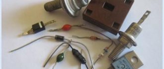
Types of Standard Rectifiers
There are various power rectifier semiconductor diodes depending on the type of installation, material, shape, number of diodes, and level of current passed. The most common are:
- Medium power devices that can transmit current from 1 to 6 Amps. Moreover, the technical parameters of most devices say that such diodes can change the current from voltage to 1.3 kiloVolt;
- Rectifier diodes of the maximum series can pass current from 10 Amps to 400, they are mainly used as ultra-fast converters for controlling industrial activities. These devices are also called high-voltage;
- Low frequency or low power diodes.
Before purchasing any devices of this type, it is very important to correctly select the basic parameters of rectifier diodes. These include: I-V characteristics (maximum reverse current, maximum peak current), maximum reverse voltage, forward voltage, case material and average rectified current. We provide a table where you can, depending on your needs, select the type of diode
The specified technical specifications may change at the request of the manufacturer, so before purchasing, check the seller’s information
We provide a table where you can, depending on your needs, select the type of diode. The specified technical specifications may change at the request of the manufacturer, so check the seller’s information before purchasing.
Photo - Table of low-frequency diodes
Imported (foreign) rectifier diodes (KVRS, SMD type):
Photo - Table of imported diodes
Data about power or high-frequency diodes:
Photo - Power diodes
Rectifier circuits are also different. They can be single-phase (for example, automotive and avalanche diodes) or multi-phase (three-phase is considered the most popular). Most low-power rectifiers for domestic equipment are single-phase, but three-phase is very important for industrial equipment. For generator, transformer, machine tools.
But at the same time, six diodes are used for an uncontrolled three-phase bridge rectifier. Therefore, it is often called a six-diode rectifier device. Bridges are considered pulsed and are capable of normalizing and rectifying even unstable current.
For low-power devices (charger), double diodes connected in series with the anode of the first diode are also connected to the cathode of the second, and are manufactured in a single housing. Some commercially available dual diodes have all four terminals available, which can be configured to suit your needs.
Photo - Medium power rectifier diode
For higher power, one discrete device typically uses each of the six bridge diodes. It can be used both for surface equipment and for monitoring more complex devices. Often six-diode bridges use limiting circuits.
Video: The principle of operation of diodes
Schottky diodes from STMicroelectronics
One of the leaders in the production of high-quality Schottky diodes is the company ST Microelecronics (hereinafter referred to as ST), one of the top ten leaders in the production of components for power electronics (See Table 1...5). A number of ST products are simply unique: for example, no one else is able to mass produce 30+30 A/170 V Schottky diodes in the TO-220 package.
Table 1. Schottky diodes for current up to 200 mA...1 A
| Diode type | Housings | [email protected] , V/A | [email protected] , V/A | UR, V | IAV, A | IFSM, A | [email protected] °C, mA | TJ max,°C | [email protected] , pF | CVC |
| BAT20J | SOD323 | 0,[email protected],1 | 0,[email protected] | 23 | 1 | 5 | 0,[email protected] | 150 | 25 | R |
| BAT30 (1x, 2x) | SOT23, SOD323/523/923 | 0,[email protected],03 | 0,[email protected],2 | 30 | 0,3 | 1 | 0,[email protected] | 150 | 8 | DёR |
| BAT60J | SOD323 | 0,[email protected],1 | 0,[email protected] | 10 | 0,5 | 5 | 0,08 | 150 | 40 | R |
| STPS0520Z | SOD123 | 0,[email protected],1 | 0,[email protected],5 | 20 | 0,5 | 5,5 | 1,[email protected] | 125 | 65 | R+ |
| STPS0530Z | SOD123 | 0,[email protected],1 | 0,[email protected],5 | 30 | 0,5 | 5,5 | 0,[email protected] | 150 | 80 | R |
| STPS0540Z | SOD123 | 0,[email protected],1 | 0,[email protected],5 | 40 | 0,5 | 5,5 | 0,[email protected] | 150 | 80 | R |
| STPS0560Z | SOD123 | 0,[email protected],1 | 0,[email protected],5 | 60 | 0,5 | 5,5 | 0,[email protected] | 150 | 45 | D- |
| TMBAT49 | MELF | 0,[email protected],01 | 0,[email protected],1 | 80 | 0,5 | 10* | 0,6 | 125 | 40 | DёR |
| TMBYV10-40 | MELF | 0,[email protected],1 | 0,[email protected] | 40 | 1 | 25 | 1 | 125 | 70 | R+ |
| TMBYV10-60 | MELF | 0,[email protected],1 | 0,[email protected] | 60 | 1 | 20 | 0,5 | 125 | 45 | D |
| 1N5817 | DO-41 | 0,[email protected],1 | 0,[email protected] | 20 | 1 | 25 | 0,6 | 150 | 120 | R |
| 1N5818 | DO-41 | 0,[email protected],1 | 0,[email protected] | 30 | 1 | 25 | 0,8 | 150 | 120 | R |
| 1N5819 | DO-41 | 0,[email protected],1 | 0,[email protected] | 40 | 1 | 20 | 0,4 | 150 | 80 | D |
| STPS120M/MF | DO-216/DO-222 | 0,[email protected],1 | 0,[email protected] | 20 | 1 | 45 | 0,15 | 150 | 150 | D |
| STPS130A/U | SMA/SMB | 0,[email protected],1 | 0,[email protected] | 30 | 1 | 45 | 0,4 | 150 | 100 | DёR |
| STPS140A/U/Z | SMA/SMB/SOD-123 | 0,[email protected],1 | 0,[email protected] | 40 | 1 | 50 | 0,6 | 150 | 80 | DёR |
| STPS160A/MF | SMA/DO-222/DO-41 | 0,[email protected],1 | 0,[email protected] | 60 | 1 | 75 | 0,15 | 150 | 100 | D- |
| STPS1150A | SMA/DO-41 | 0,[email protected],1 | 0,[email protected] | 150 | 1 | 50 | 0,02 | 175 | 38 | D- |
| STPS1L20M/MF | DO-216/DO-222 | 0,[email protected],1 | 0,[email protected] | 20 | 1 | 50 | 1 | 150 | 170 | DёR |
| STPS1L30A/U/M/MF | SMA/SMB/DO-216/DO-222 | 0,[email protected],1 | 0,[email protected] | 30 | 1 | 75 | 2 | 150 | 200 | R |
| STPS1L40A/U/M/MF | SMA/SMB/DO-216/DO-222 | 0,[email protected],1 | 0,[email protected] | 40 | 1 | 60 | 0,6 | 150 | 70 | D |
| STPS1L60A/MF | SMA/DO-222/DO-41 | 0,[email protected],1 | 0,[email protected] | 60 | 1 | 40 | 0,8 | 150 | 56 | D- |
| STPS1H100A/U/AF/MF | SMA/SMB/DO-221/DO-222 | 0,[email protected],1 | 0,[email protected] | 100 | 1 | 50 | 0,01 | 175 | 55 | D- |
| For notes on the table, see the end of the article. | ||||||||||
Table 2. Schottky diodes for currents up to 2...3 A (including dual ones, for them - the data of one diode)
| Diode type | Housings | [email protected] , V/A | [email protected] , V/A | UR, V | IAV, A | IFSM, A | [email protected] °C, mA | TJ max,°C | [email protected] , pF | CVC |
| STPS2L25U/UF | SMB/SMBF | 0,[email protected],2 | 0,[email protected] | 25 | 2 | 75 | 1,5 | 150 | 210 | DёR |
| STPS2L30A/AF/UF | SMA/SMAF/SMBF | 0,[email protected],2 | 0,[email protected] | 30 | 2 | 75 | 2,0 | 150 | 210 | DёR |
| STPS2L40AF/U/UF | SMAF/SMB/SMBF | 0,[email protected],2 | 0,[email protected] | 40 | 2 | 75 | 4,0 | 150 | 280 | D |
| STPS2L60/A/UF | DO-41/SMA/SMBF | 0,[email protected],2 | 0,[email protected] | 60 | 2 | 75 | 0,8 | 150 | 120 | D- |
| STPS2H100A/U/UF/RL | SMA/SMB/SMBF/DO-41 | 0,[email protected],2 | 0,[email protected] | 100 | 2 | 75 | 0,05 | 175 | 50 | D- |
| STPS2150A/AF | SMA/SMAF | 0,[email protected],2 | 0,[email protected] | 150 | 2 | 75 | 0,05 | 175 | 70 | D- |
| 1N5821 | DO-201 | 0,[email protected],2 | 0,[email protected] | 30 | 3 | 80 | 3,0 | 150 | 300 | DёR |
| 1N5822 | DO-201 | 0,[email protected],2 | 0,[email protected] | 40 | 3 | 80 | 1,5 | 150 | 200 | D |
| STPS3L25S | SMC | 0,[email protected],25 | 0,[email protected] | 25 | 3 | 75 | 1,5 | 150 | 200 | D- |
| STPS3L40S/UF | SMC/SMBF | 0,[email protected],3 | 0,[email protected] | 40 | 3 | 75 | 1,5 | 150 | 200 | D |
| STPS340B/S/U/UF | DPAK/SMC/SMB/SMBF | 0,[email protected],2 | 0,[email protected] | 40 | 3 | 75 | 0,25 | 150 | 150 | D- |
| STPS3L60/Q/U/UF | DO-201/DO-215/SMB/SMBF | 0,[email protected],25 | 0,[email protected] | 60 | 3 | 100 | 1,5 | 150 | 160 | D- |
| STPS3L60S | SMC | 0,[email protected],25 | 0,[email protected] | 60 | 3 | 75 | 0,8 | 150 | 100 | D- |
| STPS3H100U/UF | SMB/SMBF | 0,[email protected],25 | 0,[email protected] | 100 | 3 | 75 | 0,04 | 175 | 50 | D- |
| STPS3150/U/UF | DO-201/SMB/SMBF | 0,[email protected],3 | 0,[email protected] | 150 | 3 | 100 | 0,05 | 175 | 100 | D |
| STPS640CT/B/FPAB* | TO-220/DPAK/ISO-220 | 0,[email protected],3 | 0,[email protected] | 40 | 3 | 75 | 0,3 | 150 | 150 | R |
| STPS660CB* | DPAK | 0,[email protected],3 | 0,[email protected] | 60 | 3 | 50 | 0,3 | 125 | 350* | D |
| For notes on the table, see the end of the article. | ||||||||||
Table 3. Schottky diodes for current up to 2...3 A (including dual ones, for them - the data of one diode)
| Diode type | Housings | [email protected] , V/A | [email protected] , V/A | UR, V | IAV, A | IFSM, A | [email protected] °C, mA | TJ max,°C | [email protected] , pF | CVC |
| STPS5L25 | DPAK | 0,[email protected],5 | 0,[email protected] | 25 | 5,0 | 75 | 16 | 150 | 600 | DёR |
| STPS5L40 | DO201 | 0,[email protected],5 | 0,[email protected] | 40 | 5,0 | 150 | 5 | 150 | 300 | D |
| STPS5L60/S | DO201/SMC | 0,[email protected],5 | 0,[email protected] | 60 | 5,0 | 150 | 4 | 150 | 400 | D- |
| STPS745D/FP/G | TO220/ISO220/D2PAK | 0,[email protected],5 | 0,[email protected] | 45 | 7,5 | 150 | 0,8 | 175 | 320 | D- |
| STPS8L30B/H | DPAK/IPAK | 0,[email protected] | 0,[email protected] | 30 | 8,0 | 75 | 10 | 150 | 600 | R |
| STPS8H100G/FP/D | TO220/ISO220/D2PAK | 0,[email protected] | 0,[email protected] | 100 | 8,0 | 250 | 0,2 | 175 | 500 | D- |
| STPS10L40CT/CG/CFP* | TO220/D2PAK/ ISO220 | 0,[email protected],5 | 0,[email protected] | 40 | 5,0 | 150 | 4 | 150 | 340 | D |
| STPS10L45CT/CG/CFP/CR* | TO220/D2PAK/ ISO220/I2PAK | 0,[email protected],5 | 0,[email protected] | 45 | 5,0 | 150 | 5 | 150 | 340 | DёR |
| STPS10L60CFP/CG* | ISO220/D2PAK | 0,[email protected],5 | 0,[email protected] | 60 | 5,0 | 180 | 7 | 150 | 400 | D |
| STPS10H100CT/CFP/CG/CR* | TO220/ISO220/D2PAK/I2PAK | 0,[email protected],5 | 0,[email protected] | 100 | 5,0 | 180 | 0,08 | 175 | 340 | D |
| STPS10120CT/CFP* | TO220/ISO220 | 0,[email protected],5 | 0,[email protected] | 120 | 5,0 | 120 | 0,08 | 175 | 120 | D |
| STPS10150CT/CFP/CG* | TO220/ISO220/D2PAK | 0,[email protected],5 | 0,[email protected] | 150 | 5,0 | 120 | 0,03 | 175 | 100 | DёR |
| STPS10170CT/CG/CR/CB | TO220/D2PAK/I2PAK/DPAK | 0,[email protected],5 | 0,[email protected] | 170 | 5,0 | 75 | 0,1 | 175 | 100 | DёR |
| STPS15L30CDJF* | PQFN8 | 0,[email protected] | 0,[email protected],5 | 30 | 7,5 | 150 | 8 | 150 | 500 | D- |
| STPS15L30CB* | DPAK | 0,[email protected] | 0,[email protected],5 | 30 | 7,5 | 75 | 8 | 150 | 850 | DёR |
| STPS1545CT/CFP/ CG/CR/CB* | TO220/ISO220/D2PAK/I2PAK/DPAK | 0,[email protected] | 0,[email protected],5 | 45 | 7,5 | 150 | 0,6 | 175 | 320 | D- |
| STPS15L45CB* | DPAK | 0,[email protected] | 0,[email protected],5 | 45 | 7,5 | 75 | 5 | 150 | 520 | D- |
| STPS15L60CB* | DPAK | 0,[email protected] | 0,[email protected],5 | 60 | 7,5 | 75 | 7 | 150 | 360 | D- |
| STPS15H100CB/CH* | DPAK/IPAK | 0,[email protected] | 0,[email protected],5 | 100 | 7,5 | 75 | 0,08 | 175 | 300 | D- |
| STPS16L40CT* | TO220 | 0,[email protected] | 0,[email protected] | 40 | 8,0 | 180 | 6 | 150 | 700 | DёR |
| STPS16H100CT/CFP/CG/CR* | TO220/ISO220/D2PAK/I2PAK | 0,[email protected] | 0,[email protected] | 100 | 8,0 | 200 | 0,1 | 175 | 400 | D |
| STPS16150CT/CG/CR* | TO220/D2PAK/I2PAK | 0,[email protected] | 0,[email protected] | 150 | 8,0 | 150 | 0,05 | 175 | 160 | D- |
| STPS16170CT/CG/CR/CB* | TO220/D2PAK/I2PAK/DPAK | 0,[email protected] | 0,[email protected] | 170 | 8,0 | 75 | 0,1 | 175 | 150 | D- |
| For notes on the table, see the end of the article. | ||||||||||
Table 4. Schottky diodes for currents up to 10...25 A (including dual ones, for them - the data of one diode)
| Diode type | Housings | [email protected] , V/A | [email protected] , V/A | UR, V | IAV, A | IFSM, A | [email protected] °C, mA | TJ max,°C | [email protected] , pF | CVC |
| STPS10L25D/G | TO220/D2PAK | 0,[email protected] | 0,[email protected] | 25 | 10 | 200 | 15,0 | 150 | 1300 | DёR |
| STPS1045B | DPAK | 0,[email protected] | 0,[email protected] | 45 | 10 | 75 | 0,7 | 175 | 500 | D- |
| STPS1045D/FP | TO220/ISO220 | 0,[email protected] | 0,[email protected] | 45 | 10 | 180 | 0,8 | 175 | 500 | D- |
| STPS10L60D/FP | TO220/ISO220 | 0,[email protected] | 0,[email protected] | 60 | 10 | 220 | 6,0 | 150 | 600 | D |
| STPS15L25D/G | TO220/D2PAK | 0,[email protected] | 0,[email protected] | 25 | 15 | 250 | 20,0 | 150 | 2300 | R+ |
| STPS20L15D/G | TO220/D2PAK | 0,[email protected] | 0,[email protected] | 15 | 20 | 310 | 40,0 | 125 | 1400 | R |
| STPS20L25CT/CG* | TO220/D2PAK | 0,[email protected] | 0,[email protected] | 25 | 10 | 220 | 16,0 | 150 | 1300 | R |
| STPS2030CT/CG/CR* | TO220/D2PAK/I2PAK | 0,[email protected] | 0,[email protected] | 30 | 10 | 180 | 10,0 | 150 | 1000 | DёR |
| STPS20L40CFP* | ISO220 | 0,[email protected] | 0,[email protected] | 40 | 10 | 180 | 5,0 | 150 | 700 | DёR |
| STPS20L45CT/CFP/CG* | TO220/ISO220/D2PAK | 0,[email protected] | 0,[email protected] | 45 | 10 | 180 | 7,0 | 150 | 700 | DёR |
| STPS2045CT/CFP/CG/CR* | TO220/ISO220/D2PAK/I2PAK | 0,[email protected] | 0,[email protected] | 45 | 10 | 180 | 0,8 | 175 | 500 | D- |
| STPS20L60CT/CG/CR* | TO220/D2PAK/I2PAK | 0,[email protected] | 0,[email protected] | 60 | 10 | 220 | 7,0 | 150 | 600 | D- |
| STPS2060CT* | TO-220 | 0,[email protected] | 0,[email protected] | 60 | 10 | 200 | 0,5 | 150 | 550 | D |
| STPS20100CT* | TO-220 | 0,[email protected] | 0,[email protected] | 100 | 10 | 200 | 1,6 | 175 | 560 | D |
| STPS20H100CT/CFP/CG/CR* | TO220/ISO220/D2PAK/I2PAK | 0,[email protected] | 0,[email protected] | 100 | 10 | 250 | 0,08 | 175 | 500 | D- |
| STPS20S100CT/CFP/CR* | TO220/ISO220/I2PAK | 0,[email protected] | 0,[email protected] | 100 | 10 | 180 | 0,08 | 175 | 300 | D- |
| STPS20120D | TO220 | 0,[email protected] | 0,[email protected] | 120 | 20 | 200 | 0,25 | 175 | 370 | D- |
| STPS20120CT/CFP/CR* | TO220/ISO220/I2PAK | 0,[email protected] | 0,[email protected] | 120 | 10 | 150 | 0,15 | 175 | 200 | D- |
| STPS20L120CT/CFP* | TO220/ISO220 | 0,[email protected] | 0,[email protected] | 120 | 10 | 200 | 1,0 | 150 | 320 | D- |
| STPS20150CT/CFP/CG/CR* | TO220/ISO220/D2PAK/I2PAK | 0,[email protected] | 0,[email protected] | 150 | 10 | 180 | 0,02 | 175 | 260 | D- |
| STPS20170CT/CFP/CG/CR* | TO220/ISO220/D2PAK/I2PAK | 0,[email protected] | 0,[email protected] | 170 | 10 | 180 | 0,02 | 175 | 260 | D |
| STPS2545CT/CFP/CG* | TO220/ISO220/D2PAK | 0,[email protected] | 0,[email protected] | 45 | 12,5 | 200 | 0,7 | 175 | 600 | D- |
| STPS30L30CT/CG/CR* | TO220/D2PAK/I2PAK | 0,[email protected] | 0,[email protected] | 30 | 15 | 220 | 20,0 | 150 | 1300 | R |
| STPS3030CT/CG/CR* | TO220/D2PAK/I2PAK | 0,[email protected] | 0,[email protected] | 30 | 15 | 250 | 10,0 | 150 | 1000 | R |
| STPS30L40CW/CT/CG* | TO247/TO220/D2PAK | 0,[email protected] | 0,[email protected] | 40 | 15 | 220 | 8,0 | 150 | 650 | DёR |
| STPS30L45CW/CT/CG/CR* | TO247/TO220/D2PAK/I2PAK | 0,[email protected] | 0,[email protected] | 45 | 15 | 220 | 12,0 | 150 | 650 | DёR |
| STPS3045CW/CP/CPI/ CT/CFP/CG/CR* | TO247/TO218/ISO218/TO220/ISO220/D2PAK/I2PAK | 0,[email protected] | 0,[email protected] | 45 | 15 | 220 | 1,0 | 175 | 800 | DёR |
| STPS30L60CW/CT/CG/CR* | TO247/TO220/D2PAK/I2PAK | 0,[email protected] | 0,[email protected] | 60 | 15 | 230 | 8,0 | 150 | 800 | D- |
| STPS3060CW* | TO247 | 0,[email protected] | 0,[email protected] | 60 | 15 | 200 | 0,4 | 150 | 550 | DёR |
| STPS30H60CW/CT/CFP/CG/CR* | TO247/TO220/ISO220/D2PAK/I2PAK | 0,[email protected] | 0,[email protected] | 60 | 15 | 230 | 0,8 | 175 | 800 | D- |
| STPS30H100CW/CT* | TO247/TO220 | 0,[email protected] | 0,[email protected] | 100 | 15 | 250 | 0,1 | 175 | 500 | D |
| STPS30L120CT/CFP* | TO220/ISO220 | 0,[email protected] | 0,[email protected] | 120 | 15 | 220 | 1,0 | 150 | 500 | DёR |
| STPS30120CT/CR* | TO220/I2PAK | 0,[email protected] | 0,[email protected] | 120 | 15 | 180 | 0,2 | 175 | 300 | D- |
| STPS30150CW/CT/CFP/CG* | TO247/TO220/D2PAK | 0,[email protected] | 0,[email protected] | 150 | 15 | 220 | 0,03 | 175 | 400 | D- |
| STPS30170CW/CT/CFP/CG* | TO247/TO220/ISO220/D2PAK | 0,[email protected] | 0,[email protected] | 170 | 15 | 220 | 0,03 | 175 | 400 | D- |
| STPS40L15CW/CT* | TO247/TO220 | 0,[email protected] | 0,[email protected] | 15 | 20 | 310 | 60,0 | 125 | 1300 | R |
| STPS41L30CT/CG/CR* | TO220/D2PAK/I2PAK | 0,[email protected] | 0,[email protected] | 30 | 20 | 220 | 15,0 | 150 | 1600 | R |
| STPS40L40CW/CT* | TO247/TO220 | 0,[email protected] | 0,[email protected] | 40 | 20 | 230 | 15,0 | 150 | 1600 | R |
| STPS40L45CW/CT/CG* | TO247/TO220/D2PAK | 0,[email protected] | 0,[email protected] | 40 | 20 | 230 | 20,0 | 150 | 1500 | R |
| STPS4045CW/CT* | TO247/TO220 | 0,[email protected] | 0,[email protected] | 45 | 20 | 220 | 1,0 | 175 | 550 | D- |
| STPS41L45C T/CG/CR* | TO220/D2PAK/I2PAK | 0,[email protected] | 0,[email protected] | 45 | 20 | 220 | 10,0 | 150 | 1300 | DёR |
| STPS41L60CT/CG/CR* | TO220/D2PAK/I2PAK | 0,[email protected] | 0,[email protected] | 60 | 20 | 220 | 12,0 | 150 | 1700 | D |
| STPS40M100CT/CR* | TO220/I2PAK | 0,[email protected] | 0,[email protected] | 100 | 20 | 530 | 1,5 | 150 | 1000 | D- |
| STPS40SM100CT/CG/CR* | TO220/D2PAK/I2PAK | 0,[email protected] | 0,[email protected] | 100 | 20 | 530 | 1,0 | 150 | 750 | D- |
| STPS40H100CT/CG/CR* | TO220/D2PAK/I2PAK | 0,[email protected] | 0,[email protected] | 100 | 20 | 220 | 0,25 | 175 | 850 | D |
| STPS40H100CW* | TO247 | 0,[email protected] | 0,[email protected] | 100 | 20 | 300 | 0,6 | 150 | 1300 | D- |
| STPS41H100CT/CG/CR* | TO220/D2PAK/I2PAK | 0,[email protected] | 0,[email protected] | 100 | 20 | 220 | 0,2 | 175 | 850 | D |
| STPS40120CT/CR* | TO220/I2PAK | 0,[email protected] | 0,[email protected] | 120 | 20 | 200 | 0,4 | 175 | 470 | D |
| STPS40150CW/CT/CG* | TO247/TO220/D2PAK | 0,[email protected] | 0,[email protected] | 150 | 20 | 250 | 0,2 | 175 | 500 | D- |
| STPS40170CW/CT/CG* | TO247/TO220/D2PAK | 0,[email protected] | 0,[email protected] | 170 | 20 | 250 | 0,5 | 175 | 500 | D |
| STPS50U100CT/CR* | TO220,I2PAK | 0,[email protected] | 0,[email protected] | 100 | 25 | 250 | 1,5 | 150 | 1600* | D |
| For notes on the table, see the end of the article. | ||||||||||
Table 5. Schottky diodes for currents up to 30...120A (including dual ones, for them - the data of one diode)
| Diode type | Housings | [email protected] , V/A | [email protected] , V/A | UR, V | IAV, A | IFSM, A | [email protected] °C, mA | TJ max,°C | [email protected] , pF | CVC |
| STPS3045DJF | PQFN8 | 0,[email protected] | 0,[email protected] | 45 | 30 | 200 | 2,5 | 150 | 1200 | D |
| STPS30100ST | TO220 | 0,[email protected] | 0,[email protected] | 100 | 30 | 300 | 1,6 | 150 | 1300 | D- |
| STPS30M100ST/SFP/SR | TO220/ISO220/I2PAK | 0,[email protected] | 0,[email protected] | 100 | 30 | 300 | 2 | 150 | 1100 | D- |
| STPS30SM100ST/SFP/SG/SR | TO220/ISO220/D2PAK/I2PAK | 0,[email protected] | 0,[email protected] | 100 | 30 | 530 | 0,9 | 150 | 900 | D- |
| STPS30M100DJF | PQFN8 | 0,[email protected] | 0,[email protected] | 100 | 30 | 200 | 0,8 | 150 | 600 | D- |
| STPS30U100DJF | PQFN8 | 0,[email protected] | 0,[email protected] | 100 | 30 | 200 | 2 | 150 | 1500 | D- |
| STPS30120DJF | PQFN8 | 0,[email protected] | 0,[email protected] | 120 | 30 | 200 | 0,3 | 150 | 650 | D |
| STPS30170DJF | PQFN8 | 0,[email protected] | 0,[email protected] | 170 | 30 | 200 | 0,25 | 150 | 450 | D |
| STPS60L30CW* | TO247 | 0,[email protected] | 0,[email protected] | 30 | 30 | 600 | 30 | 150 | 2800 | R |
| STPS60L40CW* | TO247 | 0,[email protected] | 0,[email protected] | 40 | 30 | 600 | 12 | 150 | 2400 | R |
| STPS60L45CW* | TO247 | 0,[email protected] | 0,[email protected] | 45 | 30 | 600 | 12 | 150 | 2400 | R |
| STPS6045CW/CP/CPI* | TO247/TO218/ISO218 | 0,[email protected] | 0,[email protected] | 45 | 30 | 400 | 2,5 | 175 | 1600 | DёR |
| STPS61L45CT/CW* | TO220/TO247 | 0,[email protected] | 0,[email protected] | 45 | 30 | 500 | 20 | 150 | 1700 | DёR |
| STPS61L60CT/CW* | TO220/TO247 | 0,[email protected] | 0,[email protected] | 60 | 30 | 400 | 15 | 150 | 1300 | D |
| STPS60H100CT* | TO220 | 0,[email protected] | 0,[email protected] | 100 | 30 | 300 | 0,2 | 175 | 850 | D- |
| STPS61H100CW* | TO247 | 0,[email protected] | 0,[email protected] | 100 | 30 | 450 | 0,25 | 175 | 1200 | D- |
| STPS60150CT* | TO220 | 0,[email protected] | 0,[email protected] | 150 | 30 | 270 | 0,2 | 175 | 600 | D- |
| STPS61150CW* | TO247 | 0,[email protected] | 0,[email protected] | 150 | 30 | 500 | 0,6 | 175 | 1200 | D- |
| STPS60170CT* | TO220 | 0,[email protected] | 0,[email protected] | 170 | 30 | 270 | 0,6 | 175 | 1200 | DёR |
| STPS61170CW* | TO247 | 0,[email protected] | 0,[email protected] | 170 | 30 | 500 | 0,9 | 175 | 1200 | DёR |
| STPS80L60CY* | MAX247 | 0,[email protected] | 0,[email protected] | 60 | 40 | 400 | 35 | 150 | 5500 | R |
| STPS80H100CY* | MAX247 | 0,[email protected] | 0,[email protected] | 100 | 40 | 400 | 1 | 175 | 1900 | D |
| STPS80H100CTV* | ISOTOP4 | 0,[email protected] | 0,[email protected] | 100 | 40 | 700 | 1 | 150 | 1900 | D |
| STPS80150CW* | TO247 | 0,[email protected] | 0,[email protected] | 150 | 40 | 500 | 0,6 | 175 | 1300 | D |
| STPS80170CW* | TO247 | 0,[email protected] | 0,[email protected] | 170 | 40 | 500 | 1,5 | 175 | 1300 | DёR |
| STPS120L15CTV* | ISOTOP4 | 0,[email protected] | 0,[email protected] | 15 | 60 | 1200 | 340 | 125 | 6800 | D |
| STPS12045CTV* | ISOTOP4 | 0,[email protected] | 0,[email protected] | 45 | 60 | 900 | 6 | 150 | 3100 | D |
| STPS16045CTV* | ISOTOP4 | 0,[email protected] | 0,[email protected] | 45 | 80 | 900 | 6 | 150 | 3100 | D |
| STPS160H100CTV* | ISOTOP4 | 0,[email protected] | 0,[email protected] | 100 | 80 | 1000 | 2,5 | 150 | 3800 | D- |
| STPS200170CTV* | ISOTOP4 | 0,[email protected] | 0,[email protected] | 170 | 100 | 700 | 2,5 | 150 | 3800 | D- |
| STPS24045CTV* | ISOTOP4 | 0,[email protected] | 0,[email protected] | 45 | 120 | 1500 | 10 | 150 | 8500 | R |
| For notes on the table, see the end of the article. | ||||||||||
The designation of ST Schottky rectifier diodes consists of the following elements:
- prefix STPS (ST Power Shottky);
- the first number indicating the rated current in amperes;
- optional suffix (for example, H, L, M, S, SM, U) indicating the series of diodes: H - high voltage / high temperature (Tj MAX = 150 ... 175 ° C), L - low VF, U - Ultra Low VF ( for relatively high-voltage diodes);
- the second number is the permissible reverse voltage in Volts;
- optional letter designation of the connection diagram: with a common cathode - C, single in a multi-lead package - S;
- letter designation of housing type: A- SMA, AF- SMA Flat, B- DPAK, D- DO-220, DJF- PQFN8, FP- TO-220 ISO, G- D2PAK, H- IPAK, R- I2PAK, S- SMC , T-TO-220, TV-ISOTOP (SOT-227), U-SMB, UF-SMB Flat, W-TO-247, Y-MAX-247, Z-SOD123.
Example: STPS160U is a 1 A, 60 V Schottky diode in an SMB package.
When choosing Schottky diodes, it is necessary to clearly distinguish between two groups of applications - relatively low-frequency switching (OR-ing of power supplies, voltage summing, 50/60 Hz rectification with minimal losses), where minimal losses from direct voltage drop and/or leakage currents are required, and application in high-frequency pulse converters, where the minimum value of total losses is important, that is, a minimum sum of static and dynamic losses is needed.
Diodes optimized for the first group of applications are diodes with minimal forward voltage drops, usually obtained due to large junction areas (large capacitances), or special chips using a controlled MOSFET that look like a diode, but with extremely low voltage drop. MBRB2515 product with a VF of ~250 mV at 56 A, and a junction capacitance approaching 10 nF. A diode of a similar class from ST is STPS40L15CT, dual and with approximately half the junction capacitance. An example of the second approach is a diode from ST SPV1001T40, VF ~80...100 mV at a current of 5...6 A, 230...250 mV at a current of 15 A. The advantage of this solution from ST is obvious.
As for Schottky diodes for use in DC/DC converters, a diode with a minimum VF will not necessarily provide the minimum total loss. Especially with a wide range of loads (when it is necessary to take into account losses not only from direct voltage drop, but also from leakage currents - their value exponentially depends not only on temperature, but also on the initial voltage drop). This is due to the fact that in order to reduce the forward voltage drop one has to pay either by an increase in the junction area (and diode capacitance, which leads to an increase in switching losses proportional to fґСдU2/2), or by a sharp increase in the leakage current (when almost zero is selected to minimize the forward voltage drop threshold voltage due to selection of metal-semiconductor contact material). An example of a diode that has minimal capacitances, but a small range of operating currents and temperatures, is the supplied NXP PMEG1030 (3 A, 10 V), the reverse current of which at a junction temperature of 25 ... 30 ° C is about 1 mA, but at 125 ° C it reaches about 100 mA (this is not a typo!).
ST Microelectronics, as one of the leaders in power electronics, offers perhaps the widest range of Schottky diodes in the industry for currents from 0.5 to 200 A, optimized for the ratio of static and dynamic losses.
Let us pay attention, for example, to the ULVF series. STPS50U100C is a dual (25+25 A) 100 V diode in a TO-220 package, which has both a low forward voltage drop (~600 mV at 15 A/diode) and moderate leakage currents (~10 mA at 125°C) and and junction capacitance (~2200 pF at 0 V, ~1500 pF at 10 V, with a sharp decrease above 20 V, down to 300 pF at 100 V). The switching losses of each such diode at a frequency of 100 kHz are tenths of a watt, and at a frequency of 500 kHz - units of watts.
Further, for the currently popular most compact applications, ST produces a series of 15/30 A diodes in a Power Flat surface mount package (PQFN8) - its height is slightly more than 1 mm, its plan size is 5x6 mm. These are STPS15L30CDJF (7.5+7.5 A), STPS3045DJF, STPS30M100DJF, STPS30U100DJF, STPS30120DJF, STPS30170DJF. These diodes are designed for use in printed circuit boards with low thermal resistance, for example, on a metal base.
For high current applications, ST produces the highest power Schottky diodes available in the TO-220 ( STPS40M100CT, STPS40120CT, STPS50U100C, STPS60H100CT, STPS60150CT, STPS60170CT, STPS61L45CT, STPS61L60CT ) and TO-247/MAX247 ( packages 0CW, STPS80L60CW, STPS80H100CY, STPS80150CY, STPS80170CY ) . The presence of such powerful diodes in standard, widely used packages makes it possible to simplify and reduce the cost of the design of devices using them.
For applications requiring even higher currents, ST produces dual diodes in an insulated ISOTOP/ISOT4D (SOT227) package - STPS80H100TV, STPS120L15TV, STPS12045TV, STPS160H100TV, STPS24045TV, STPS200170TV (current up to 100...120 A per diode, voltage 15...170 V ).
At the other end of the range are diodes optimized for low power applications, such as the STPS0520Z (0.5 A, 20 V) - capacitance ~120 pF at 1 V, ~35 pF at 20 V, VF ~320...350 mV at 0.5 A , leakage current ~80 μA at a junction temperature of 30°C and ~5 mA at 100°C. Due to their small capacitances and moderate leakage, such diodes are a very useful component for the most common relatively low-power converters. Small capacitances allow you to increase the operating frequency without compromising efficiency. Diodes BAT30, TMBAT49, TMBYV10-40, TMBYV10-60, BAT20, BAT60 have a similar area of application.
Naturally, in addition to these “branded” products, ST produces analogues of popular standard products, from BAT30-0X, BAT41, BAT42, TMBAT49, TMBYV10-40, TMBYV10-60, BAT60, 1N5817-1N5819, 1N5821-1N5822, to MBR20100 ( STPS20S100C ) .
A very significant feature of most Schottky diodes from ST is the detailed regulation of dynamic thermal parameters and operation in avalanche breakdown mode (absorption of surge surges that arise, for example, on installation inductances). This allows the use of diodes with a lower permissible reverse voltage, obtaining benefits either in the form of reduced losses (due to lower VF and/or CD) or reduced cost of components. Savings on the cost of diodes are possible due to the fact that instead of diodes with a higher maximum voltage, you can often choose a diode designed for a lower maximum voltage and maximum current, but providing at a given operating current the same value of losses and VF as a higher voltage one, designed for a larger current. As a result, it turns out that you can either reduce losses in rectifiers by about 20...25%, or reduce the cost of the diodes used by approximately the same amount.
However, the author would like to warn against a common mistake - trying to use Schottky diodes “at the limit” of current, especially in circuits with “hard” current switching. Firstly, this is extremely undesirable from the point of view of dynamic losses, since at high currents (corresponding to voltage drops of more than 0.6 ... 0.9 V depending on the type of diode) in the structure of Schottky diodes, a parallel-connected pn transition “guard” diode begins to work . This is primarily manifested by the appearance of an accumulation of turn-off charge, which can cause large pulse currents/voltages.
Secondly, you need to remember that heating Schottky diodes has almost no effect on the forward voltage drop at high currents, but causes a sharp increase in leakage currents. The latter is dangerous due to the manifestation of the self-heating effect by reverse currents. The increased heatsink size required to avoid this risk often ends up costing more than using higher current diodes with lower static losses. Normalizing the avalanche characteristics of ST diodes in this regard turns out to be very useful, since it allows you to get by with diodes with a minimum reverse voltage (and, accordingly, both cheaper and having a lower VF).
In conclusion, it is worth saying that the range of high-speed rectifier diodes produced by ST is not limited to Schottky diodes. ST produces a large number of Ultrafast diodes (trr ~50...80 ns), including high-voltage ones (for voltages up to 1200 V) and currents up to 60 A/diode, 120 A per package ( STTH ). In some cases, their use provides even lower dynamic losses than Schottky diodes (due to lower junction capacitances), see, for example, the PFC structure described in US pat. No. 6987379.
Naturally, the ST production program also includes a large number of “small-signal” Schottky diodes, such as BAS70-0X, BAR18, TMM6263, TMMBAT41...43, TMMBAT46, TMMBAT48, BAT54.
It is also worth noting that many manufacturers still consider it unnecessary to provide SPICE models of their diodes. You can get them from ST on their website. The quality of these models, of course, is not ideal, but they are quite suitable for estimation calculations with “engineering accuracy”, i.e. with errors of no more than 10...20%.
Device
A semiconductor diode is a two-terminal device made from a semiconductor substance that allows current to pass in one direction and virtually no current in the other.
The main element of the diode is a crystalline component with a pn junction, to which a metal anode and a cathode are soldered (welded). The passage of direct current is carried out when a positive potential, relative to the cathode, is applied to the anode.
Note! Holes move in the direction of forward current. The electrons move in the opposite direction
The diode design can be point, planar, or polycrystalline.
Device of a point and planar p/p device
Additional Information. There are no fundamental differences between point and planar bipolar devices.
The structure of a point diode is shown in figure (a).
When a thin needle, with an impurity deposited on it, is welded to a semiconductor plate with a certain type of electrical conductivity, a hemispherical mini pn junction with a different type of conductivity is formed. This action is called diode forming.
The production of a planar two-terminal network is carried out by the diffusion fusion method. Figure (b) shows an alloy germanium diode and the principle of its design. In a plate of n-type germanium, when a drop of indium is fused there at 500 degrees, a layer of p-type germanium is formed. The lead contacts soldered to the germanium and indium base plate are made of nickel.
Germanium, silicon, gallium arsenide and carbide are used in the production of semiconductor wafers. Semiconductor monocrystalline wafers with a correct structure throughout the entire volume are used as the basis for point and planar two-terminal networks.
In polycrystalline two-terminal networks, the pn junction is formed by semiconductor layers, which include a large number of randomly oriented small crystals that do not represent a single single-crystalline form. These are selenium, titanium and copper oxide bipolars.
Fast diodes
Fast recovery diodes are divided into diodes with a “thin base” using epitaxial-planar technology (fast-FRED and ultrafast-FRED) and Schottky diodes [6, 7]. The latter, in turn, can be traditional silicon or based on silicon carbide (SiC). Schottky barrier diodes (Schottky diodes, or DS) use a metal surface contact with a semiconductor instead of a pn junction. At the point of contact, semiconductor layers depleted of charge carriers appear, which are called gate layers. Schottky diodes differ from pn junction diodes in the following parameters:
- lower forward voltage drop UFM;
- lower reverse voltage URRM;
- higher leakage current (reverse current) IR;
- There is almost no reverse voltage charge QR.
In Schottky diodes (DS), the forward voltage drop is a function of the reverse voltage. In modern DS, the maximum reverse voltage is about 150-200 V, and the forward voltage drop is 0.2-0.35 V less than that of pn-junction diodes. DS are indispensable when designing powerful low-voltage devices (in practice, up to 27-48 B) and high-current high-frequency rectifiers due to properties a) and d).
High-speed diodes are characterized by the same basic parameters that are given for rectifier diodes. The important parameter I2t, equivalent to the instantaneous energy on the diode (with a specific forward resistance), is not indicated at all in domestic specifications or specifications. For foreign diodes, this parameter is not indicated for all diodes. Meanwhile, when overcurrent occurs and the real response time of the protection of power devices is taken into account, this parameter must certainly be taken into account and controlled when designing the control system. There are cases when, for example, in high-frequency power supplies, foreign diodes that are excellent in their parameters, selected with a margin only according to the permissible values of IF(AV), IFSM, failed. This seemed inexplicable, but, in our opinion, it occurred during significant current overloads or short circuits due to insufficient performance of the current protection unit.
The recovery time of the reverse resistance of the diode trr is the main parameter of high-speed diodes, which determines their inertial properties. When the polarity of the voltage applied to the diode changes, the reverse current of the diode can increase tens of times. The value of trr to a certain extent depends on the “softness” (“smoothness”) of the recovery characteristic and is normalized at a specific value of the forward current and reverse current. It should be noted that the data sheets do not always indicate the URR and IF(AV) values at which the trr value is determined, as well as the reverse resistance recovery graph. Due to the finite (non-zero) value of trr, dynamic power losses on the diode additionally occur. If the choice of diodes is incorrect in terms of the value trr and the switching frequency fk in the control system, the dynamic losses increase significantly with increasing frequency. This is especially important in devices such as pulsed power sources, various high-frequency inverters and converters, for example for portable welding units, etc.
Smooth current switching depends on the ratio of the time tb required to establish the reverse bias voltage of the diode to the time of propagation of the depletion region into the drift region ta [6]. The problem of ensuring an acceptable tb/ta ratio by developers of powerful components is being solved successfully. Thus, in 2007, Fairchild Semiconductor (Fairchild) [17] released diodes such as FFP08S60S and FFPF08S60S (Stealth II series) with excellent smooth switching (tb/ta>1.3) with a low reverse recovery time (trr<25 ns) at a breakdown voltage of 600 V. This company also released the FFPF08H60S diode of the Hyperfast II series with a reverse recovery time trr<35 ns at a breakdown voltage of 600 V and VFM<2.1 V.
Among diodes with a low VFM value, we note the new generation of ultra-fast diodes of the HiPerFRED2 series recently released by IXYS [6, 14]. The diodes are designed for a voltage of 200-400 V and a direct current of 10-120 A. At the same time, different design options are provided: DPF type diodes with low on-state losses and DPG type - for high-frequency devices. The reverse recovery time of the series diodes is 35 ns, the forward voltage drop is 0.98-1.22 V. We also note high-power diodes from Westcode [15, 16]. Westcode was founded in 1920 in the UK and currently develops and supplies high power power semiconductors. Westcode specialists also carry out the development and production of specialized modules according to the customer’s instructions using the latest testing methods [15]. The company is part of the IXYS Corporation.
Table 2 shows the characteristics and features of some high-speed diodes. Diodes and assemblies from leading foreign companies IR, IXYS, Fairchild, Westcode are presented [1, 13-18]. Domestic diodes and assemblies are represented by the products of JSC Voronezh Semiconductor Device Plant - S (JSC VZPP-S) [19]. In particular, diodes KD644 A(AS)-Zh(ZhS) for voltages of 200-700 V, currents of 25 A (2×25 A) and with a recovery time trr = 50-75 ns. A big step forward of JSC "VZPP-S" and domestic power electronics in general is the production of high-speed power modules of the MDCH-ХХ-ХХХ type for voltages of 400-700 V, currents from 60 A (2×60 A) to 100 A (2×100 A) and with a speed (trr) of the order of 100 ns. The modules are implemented in TO-244 packages (modifications 2 and 3) with a thermal resistance RthJC = 0.35-0.5 °C|W.
Application of diodes
One should not think that diodes are used only as rectifiers and detectors. In addition, you can highlight many more of their professions. The current-voltage characteristics of diodes allow their use where nonlinear processing of analog signals is required. These are frequency converters, logarithmic amplifiers, detectors and other devices. Diodes in such devices are used either directly as a converter or form the characteristics of the device when included in the feedback circuit. Diodes are widely used in stabilized power supplies, as reference voltage sources (zener diodes), or as switching elements of storage inductors (pulse voltage stabilizers).
Rectifier diodes.
Using diodes it is very easy to create signal limiters: two diodes connected back-to-back - in parallel serve as excellent protection for the input of an amplifier, for example, a microphone, from supplying an increased signal level. In addition to the listed devices, diodes are very often used in signal switches, as well as in logic devices. It is enough to recall the logical operations AND, OR and their combinations. One type of diode is LED. Once upon a time they were used only as indicators in various devices. Now they are everywhere, from the simplest flashlights to TVs with LED backlighting, it is simply impossible not to notice them.
Diode parameters
Diodes have a lot of parameters and they are determined by the function they perform in a particular device. For example, in diodes that generate microwave oscillations, a very important parameter is the operating frequency, as well as the cutoff frequency at which the generation fails. But for rectifier diodes this parameter is completely unimportant. The main parameters of rectifier diodes are shown in the table below.
Table of main parameters of rectifier diodes.
In switching and switching diodes, the switching speed and recovery time, that is, the speed of full opening and full closing, are important. In high-power power diodes, power dissipation is important. To do this, they are mounted on special radiators. But diodes operating in low-current devices do not need any radiators. But there are parameters that are considered important for all types of diodes, we list them:
- U pr. – permissible voltage on the diode when current flows through it in the forward direction. You should not exceed this voltage, as this will lead to its damage.
- U rev. – permissible voltage on the diode in the closed state. It is also called breakdown voltage. In the closed state, when no current flows through the pn junction, a reverse voltage is formed at the terminals. If it exceeds the permissible value, this will lead to a physical “breakdown” of the pn junction. As a result, the diode will turn into an ordinary conductor (burn out).
Schottky diodes are very sensitive to excess reverse voltage, which very often fail for this reason.
Conventional diodes, for example, silicon rectifiers, are more resistant to excess reverse voltage. When it is slightly exceeded, they go into a reversible breakdown mode. If the diode crystal does not have time to overheat due to excessive heat generation, then the product can work for a long time.
- I ave. – direct current of the diode. This is a very important parameter that should be taken into account when replacing diodes with analogues or when designing homemade devices. The magnitude of the forward current for different modifications can reach tens and hundreds of amperes. Particularly powerful diodes are installed on the radiator to remove heat, which is formed due to the thermal effect of the current. The PN junction in direct connection also has low resistance. At small operating currents its effect is not noticeable, but at currents of a few to tens of amperes the diode crystal heats up noticeably. For example, a rectifier diode bridge in an inverter welding machine must be installed on a radiator.
- I return – reverse current of the diode. The reverse current is the so-called minority carrier current. It is formed when the diode is closed. The amount of reverse current is very small and in the vast majority of cases it is not taken into account.
- U stabilization – stabilization voltage (for zener diodes). Read more about this parameter in the article about zener diode.
In addition, it should be borne in mind that all these parameters in the technical literature are printed with the “max” symbol. The maximum permissible value of this parameter is indicated here. Therefore, when choosing the type of diode for your design, you must count on the maximum permissible values.
High current diodes.
Low Frequency Rectifier Diodes and Bridges
Rectifier diodes contain a single pn junction and are relatively simple semiconductor devices. Depending on the operating frequency (speed), such diodes are divided into low-frequency (up to 1 kHz), high-frequency and pulsed (high-speed). When presenting this section, we will consider only low-frequency diodes. Other groups of diodes are discussed in the next section. Main parameters of rectifier diodes [7]:
- maximum permissible reverse repetitive voltage URRM;
- maximum permissible rectified direct average/direct effective (rms) current - IF(AV)/IF(RMS);
- maximum permissible pulse current IFMS - for repeated or single pulses of diodes (in particular, for 10 ms - half a frequency period of 50 Hz or for 8.3 ms - for a frequency of 60 Hz);
- direct voltage drop across the turned on UFM diode;
- permissible operating frequency fmax.
The maximum permissible power dissipation, as a rule, is not specified and is determined by standard types of diode packages (with certain values of junction-case thermal resistance Rth JC). In most cases, rectifier diodes are attached to the heat sink (cooler), and in the case of a tablet housing design, on both sides. Heat removal is provided by natural convection or forced ventilation.
For network rectifiers, rectifier diodes or bridges with voltage URRM = 600-800 V for single-phase (~220/230 V) and 800-1000 V for three-phase (3×~220 V or 3×~380 V) AC mains are usually selected [ 8]. In this case, the maximum increase in the mains voltage (by +20%), possible “distortions” of the mains phase voltages, etc. are taken into account. In this case, it is especially important to ensure the insulation voltage of the terminals relative to the unit body, which should be Uisol≥2000 V.
Note that, unlike other power components, Russian developers and manufacturers much more often use power rectifier diodes from domestic companies in control systems. Domestic low-frequency diodes have well-developed technology, are quite reliable and relatively inexpensive, for example, diodes of the D1XX series (D106-, D112-, D122-, etc.), D2XX (D232-), D3XX (D333), etc. These diodes cover the voltage range URRM = 100-6000 V and currents IF(AV) = 10-6600 A. The diodes are available in pin (metal-glass housings SD1-SD3, metal-ceramic housings SD4-SD7), tablet and modular versions. One of the main manufacturers of power diodes and power electronics components in general is JSC Elektrovypryamitel (Saransk) [9]. The supply of diodes is carried out by many dealer companies: Symmetron LLC, Platan LLC, Power Diode LLC (Moscow), etc. In particular, a very wide range of power diodes is supplied by Energosistemavtomatika LLC (Moscow) [ 10].
Table 1 shows the main parameters of some low-frequency rectifier diodes from domestic companies.
Since rectifier bridges are assembled from rectifier diodes, they naturally have a similar set of parameters. But since the bridge has 2 diodes connected in series in each half-cycle of the alternating voltage, the UFM parameter naturally has a greater value. Let us give as an example the parameters of IR bridges:
- single-phase bridge 26MBxxA: URRM = 200-800 V, IF(AV) = 25 A, IFSM = 475 A (10 ms), UFM = 1.1 V; housing D-34 A;
- three-phase bridge 110MT120KB: URRM = 1200 V, IF(AV) = 110 A, IFSM = 950 A (10 ms), threshold voltage UFM0 = 0.81 V; body - module.
Diode bridge
A diode bridge is a compact circuit that is made up of four diodes and serves the purpose of converting AC to DC. The bridge circuit makes it possible to pass current in each half-cycle, which distinguishes it favorably from the half-wave circuit. Diode bridges are produced in the form of small-sized assemblies, which are enclosed in a plastic housing.
At the output of the housing of such an assembly there are four pins marked “+”, “—
" or "
~
" to indicate the purpose of the contacts. However, diode bridges are also found not in an assembly; they are often assembled directly on a printed circuit board by connecting four diodes. The rectifier, which is performed on a diode bridge, is called full-wave.
Systematization of diodes
Classification is carried out according to purpose, physical and electrical, characteristics, material of manufacture, design and technological parameters, etc.
According to power indicators they are:
- Low-power – up to 300 mA;
- Medium power – range 300 mA-10 A;
- High power - over 10 A.
Varicaps can be made from silicon or germanium. The most common are flint elements, since they have higher technical parameters. At the same voltage values, they have much lower reverse currents, so the potential reverse voltage can register 1500V, while germanium models only have from 100V to 400V.
They also differ in their performance characteristics at different temperatures: silicon can withstand loads in the range from -60 to + 150 C, and germanium from -60 to +85 C (at maximum temperature, electron-hole pairs are formed, which contribute to the growth of the reverse current, making the diode is ineffective).
Types of varicaps
According to their area of application and method of operation, power diodes are divided into:
- General purpose – have a high reverse voltage (50V-5kV) and forward current (10A-5kA). Most often they are present in industrial networks with an oscillation frequency of 50 Hz. They can be in pin or tablet form;
- Pulse (fast-restoring) - voltage is transmitted in pulses. They differ from other types: recovery time, that is, the period of switching direct voltage to reverse; establishment time - the flow of direct current to a specific voltage; the highest recovery current is the reverse current that moves through the varicap after the switching is completed.
- Reversed - characterized by a large concentration of impurities in the p-n-region. Reverse connection occurs with low resistance, while direct connection with high resistance. They are used in devices where it is necessary to rectify small pulses with small amplitude;
- Schottky diodes - forward current is caused by the movement of electrons. For their production, low-resistance n-silicon substrates and a thin layer of high-resistance similar conductor are used. The metal electrode can rectify currents up to 10A, but does not inject minority carriers, which makes Schottky devices low-inertia.
RESPONSIBILITY
RESULTS RESULTS , , , Ñ ÑабоÑÑ Ð² какой-либо ÑÑеме.
REPORT:
- I max â пÑÑмой Ñок, коÑоÑÑй макÑималÑно доР¿ÑÑÑим, R.
- U max â обÑаÑное напÑÑжение, коÑоÑое Ð¼Ð°ÐºÑ regurgitation, R.
- I обÑÐ°Ñ â обÑаÑнÑй Ñок поÑÑоÑннÑй, мкÐ.
- U ›
- RESULTS, RESULTS.
- RESULTS, REPRESENTATION.
- max swear.
RESEARCH RESULTS Ñком. RESULTS оÑÑаÑоÑно.
Welding Application
Any transformer or inverter contains power diodes. They are designed to rectify alternating current. To increase the efficiency, the diodes are connected in a bridge circuit, in which case both half-cycles fall on the load.
In a transformer welding machine, rectifier diodes are installed at the output of the secondary winding. Welding equipment has a step-down transformer; accordingly, the no-load voltage is significantly lower than the input voltage, so high-power and low-frequency devices are required here. B200 rectifier diodes (maximum current 200A) are suitable for this.
The welding inverter requires two rectifiers. One is located at the input of the power source. It converts alternating current 220 volts 50 Hz into direct current, which is further converted into alternating current of high frequency (40-80 kHz).
With a device power of 5 kW, the rectifier diodes should have a reverse voltage of 600-1000 V and an average forward current of 25-35 A at a frequency of 50 Hz.
The second rectifier is located after the high-frequency transformer. Here the requirements are different. The maximum forward current must be at least 200 A at a frequency of 80 kHz, and the reverse voltage must exceed the open circuit voltage (60-70 V).
In any case, diodes from the powerful category are used, with a platform for mounting a radiator, since without heat removal the device will quickly burn out.
Power classification
The power of the elements is determined by the maximum permissible direct current. In accordance with this characteristic, the following classification has been adopted:
- Low-current rectifier diodes, they are used in circuits with a current of no more than 0.3 A. The housing of such devices is usually made of plastic. Their distinctive features are light weight and small dimensions.
Low Power Rectifier Diodes - Devices designed for average power can operate with current in the range of 0.3-10 A. Such elements, for the most part, are made of metal housing and equipped with rigid leads. On one of them, namely on the cathode, there is a thread that allows you to securely fix the diode on the radiator used for heat removal. Medium power rectifier diode
- Power semiconductor elements, they are designed for direct current over 10 A. Such devices are produced in metal-ceramic or metal-glass housings of the pin type (A in Fig. 4) or tablet type (B).
Rice. 4. High power rectifier diodes
Thyristors
These parts are widely used in devices for rectifying and converting electric current, welding machines, devices for starting and controlling the speed of electric vehicles, various radio-electronic and switching installations. They are also used in structures designed to compensate for reactive power loads.
Important! Low-frequency thyristors are designed for operation at a frequency of no more than 100 hertz. Devices characterized by increased performance are designed for use in installations that require a rapid increase in open electric current and closed voltage
Thyristor part
Power diodes - application
The devices are used in almost all modern household and industrial electrical appliances, for detectors, circuitry, stabilizers, switches, limiters, etc. They are used in devices for nonlinear processing of analog pulses and provide the flow of the main signal. Power diodes are used to reorganize alternating current into direct current.
Some types can be used to stabilize the output voltage of power generators or to limit the range of pulse fluctuations. Diode bridges allow you to close and open a circuit to transmit a signal in switching devices powered by electricity. Due to their technical characteristics, they are used in all products: from the simplest to the most complex.
Characteristics
Each type of semiconductor has its own operating and limiting parameters, which are selected in order to ensure operation in any circuit.
Parameters of rectifier diodes:
- I direct max
- direct current, which is the maximum permissible, A. - U reverse max
- reverse voltage, which is the maximum permissible, V. - I reverse
- constant reverse current, µA. - U direct
- direct voltage constant, V. - Operating frequency
, kHz. - Operating temperature
, C. - P max
is the maximum permissible power dissipated by the diode.
The characteristics of rectifier diodes are far from exhausted by this list. However, they are usually sufficient to select a part.
Diode rectifier parameters
Each type of diode has its own maximum permissible and performance characteristics. The main parameters of rectifier diodes are presented in the table:
As a rule, this information is accessed when an element from the rectifier circuit is unavailable and a replacement needs to be found. In most cases, analogues are selected according to the first five parameters from the table, but sometimes it is also necessary to take into account such characteristics of rectifier diodes as operating temperature and frequency.
A very important parameter of diodes is their forward current. It should be taken into account when replacing the original diodes with analogues, as well as in the case of creating homemade devices. Depending on various modifications, forward current values can reach values of several tens and even hundreds of amperes. Therefore, in powerful devices, diode bridges must be installed in a special housing together with a cooling radiator, which does not allow the crystal in the diode to overheat.
Some subtypes of diodes, such as Schottky, are very susceptible to reverse voltage surges and can therefore quickly become unusable. But silicon semiconductors, on the contrary, are resistant to increases in reverse voltage. They can last for a long period, namely until the crystal on the conductor overheats and fails, which takes a lot of time.
Manufacturing technology
The design of a rectifying diode is a wafer of a semiconductor crystal, in the body of which there are two regions with different conductivities. This is the reason why they are called planar.
Semiconductor rectifier diodes are made like this: in the region of the semiconductor crystal with n-type conductivity, aluminum, indium or boron is melted, and in the region of the crystal with p-type conductivity, phosphorus is melted.
When exposed to high temperatures, these two substances are firmly fused to the semiconductor base. In addition, the atoms of these materials diffuse into the crystal to form a region with predominantly electronic or hole conductivity. As a result, a semiconductor device is formed that has two regions with different types of electrical conductivity, and a pn junction is formed between them. This is the operating principle of the vast majority of planar diodes made of silicon and germanium.
Operating principle
The necessary effect during operation of the device is created by the features of the pn junction. They consist in the fact that a layer is built near the junction of two semiconductors, which is characterized by two points: high resistance and the absence of charge carriers. Further, when this barrier layer is exposed to alternating voltage from the outside, its thickness decreases and subsequently disappears. The current that increases during this is the direct current that passes from the anode to the cathode. If the polarity of the external alternating voltage changes, the blocking layer will be larger and the resistance will inevitably increase.
The current-voltage characteristic of the rectifier diode (volt-ampere characteristic) also gives an idea of the specifics of the rectifier’s operation and is nonlinear. It looks like this: there are two branches - forward and reverse. The first reflects the highest conductivity of the semiconductor when a direct potential difference occurs. The second indicates the value of low conductivity at an inverse potential difference.
The current-voltage characteristics of the rectifier are directly proportional to the temperature, with an increase in which the potential difference decreases. Electric current will not pass through the device in the case of low conductivity, but an avalanche breakdown occurs if the reverse voltage increases to a certain level.