Capacitive, inductive-capacitive, active smoothing filters. Schemes, properties, online calculator.
We talked thoroughly on the previous page about different types of diode rectifiers, exchanged a couple of phrases on the topic of the simplest capacitive filters, and the question of achieving the Kp within 10 -5. 10 -4 just hung in the air - the nominal capacity of the smoothing capacitor turns out to be very considerable.
The ripple factor of the rectified voltage Kp is the most important parameter of the rectifier. Its numerical value is equal to the ratio of the amplitude value of the pulsating voltage to its constant component. Let me remind you of the excerpt from the printed publication given on the previous page:
“The ripple coefficient is chosen independently depending on the expected load, allowing for direct current power supply of a very specific “purity”: 10 -3. 10 -2 (0.1-1%) – small-sized transistor radios and tape recorders, 10 -4. 10 -3 (0.01-0.1%) – radio and intermediate frequency amplifiers, 10 -5. 10 -4 (0.001-0.01%) – preliminary stages of audio frequency amplifiers and microphone amplifiers.”
In addition, the concept of filtering coefficient (smoothing coefficient) can be used in the characteristics of rectifiers. The filtering coefficient, also known as the smoothing coefficient , is a value numerically equal to the ratio of the ripple coefficient at the filter input to the ripple coefficient at the filter output Kc = Kp-in/Kp-out . For multi-link filters, the filtration coefficient is equal to the product of the filtration coefficients of individual links.
In low-current circuits, the issue of reducing ripple is solved easily and radically - by using integral stabilizers. The ripple suppression parameter (Ripple Rejection) for such mass-produced ICs is at least 50 dB (360 times the voltage), which, with a high “purity” of the output voltage, makes it possible to reduce the capacitance of electrolytes by 5-10 times.
If the developer does not have the opportunity (or desire) to include voltage stabilizers in the device, then inductive-capacitive or active smoothing filters .
Let's start with filters made of inductive elements - chokes and capacitive elements - capacitors.
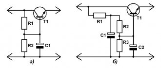
Fig.1
Figure 1a shows a diagram of the simplest capacitive anti-aliasing filter. The principle of operation is the accumulation of electrical energy by the filter capacitor and the subsequent release of this energy to the load.
In order not to be limited to 50 Hz power supplies, but also to be able to calculate filters for pulsed UPSs, I will give universal formulas that take into account the frequency of the input signal F : C1 = In/(3.14×Un×F×Kp) for half-wave rectifiers and С1 = In/(6.28×Un×F×Kp) – for full-wave. Kp is the ripple coefficient equal to the ratio of the amplitude value of the pulsating voltage to its constant component, and F is the frequency of the alternating voltage at the input of the diode rectifier.
Let's move on to inductive-capacitive LC filters. ATTENTION. The need for this kind of circuits arises exclusively in cases where it is necessary to obtain a low level of ripple in sufficiently powerful network power supplies, or in high-frequency switching UPSs. This is due to the fact that for the LC filter to operate effectively, the inductive reactance of the XL coil at the suppression frequency tends to be significantly greater than Rн. And this, in turn, leads to the fact that under conditions of low frequencies and low currents (high Rн), the inductance of the inductor turns out to be unreasonably high.
An L-shaped inductive-capacitive LC filter of the 2nd order (Fig. 1b) has significantly better filtering properties compared to a conventional capacitive one. The product LC (H*μF) depends on the required filter smoothing coefficient and is determined by the approximate formula: L1(H)×C1(μF) = 25000/(F 2 (Hz)×Kp) for half-wave rectifiers and L1×C1 = 12500/ (F 2 × Kp) – for full-wave, where C1 (μF)/L1 (mH) = 1000/Rn 2 (Ohm) .
The diagram of a U-shaped LC filter is shown in Fig. 1c. The smoothing effect of a U-shaped LC filter can be simplified as the combined action of the two filters described above, and the smoothing coefficient as the product of the smoothing coefficients of the links: capacitive and L-shaped inductive-capacitive. Chebyshev LC filters have the best filtering properties. Let's write the formula based on the recommendations set out on the page link to the page: C1 = C2; C1(μF)/L1(mH) = 1176/Rn 2 (Ohm) .
You can reduce the ripple voltage at the output of a single-link U-shaped LC filter by connecting a non-polar capacitor C3 (Fig. 1d) in parallel with inductor L1 (Fig. 1d) , which, together with the inductance of the coil, forms a notch filter. If the capacitance of capacitor C3 is chosen such that the resonant frequency of the circuit L1-C3 is equal to the ripple frequency (F for half-wave rectification or 2F for full-wave rectification), then most of the ripple voltage will be retained by this circuit and only a small amount will go to the load. So: C3 = 1/(39.44×L1×F 2 ) for half-wave rectifiers and C3 = 1/(9.86×L1×F 2 ) for full-wave rectifiers. All other element values are the same as in the previous diagram.
Let's spice up the material covered with an online table.
CALCULATOR FOR CALCULATING ELEMENTS OF THE POWER SUPPLY COLORING FILTER.
Transistor filters , compared to capacitive smoothing filters, have smaller dimensions, weight and a higher ripple smoothing coefficient. They make it possible to reduce the value of the smoothing capacitor by a factor of ten (at the same ripple level), or to reduce the pulsation amplitude by a similar number of times with a constant capacitance value.
Fig.2
Figure 2a shows a diagram of the most common transistor filter.
The high ripple voltage supplied to the transistor's collector is essentially the supply voltage to the emitter follower formed by T1. At the same time, the base circuit is powered through bias resistors and the integrating circuit R1C1, which smoothes out voltage ripple at the base. The larger the time constant T=R1C1, the less voltage ripple at the base, and since the device is an emitter follower, the ripple at the filter output will be as small as at the base. In order to reduce the dependence of the voltage at the filter output on the level of transmitted power, the current through the divider R1R2 is selected 5...10 times greater than the current branching into the base with minimal load resistance. When calculating the ratings of the divider elements, one should proceed from the voltage at the base of the transistor: Ub = Uin – Uin ripple – (2.5. 3V) . In this case, the control transistor will operate in the active mode, and the voltage drop across it will be: Uke = Uin ripple + (3.1. 3.6V) . The lower the DC voltage drop across the power transistor, the greater the efficiency of the transistor filter. It is clear from the formula that to ensure high efficiency of an active smoothing filter, a voltage already filtered to a certain level should be supplied to the input of the device . In practice, this is done by connecting a simple capacitive filter to the input (Fig. 1a), the ripple level of which can be calculated using the calculator above.
The effectiveness of active anti-aliasing filters directly depends on the gain of the transistor. The higher the h21 of the semiconductor, the larger the values of the resistors R1, R2 can be chosen - the better filtering properties the circuit will have. Therefore, in this situation, you should not even consider transistors with h21<50. But at the same time, composite transistors with high gain are also not the optimal choice due to increased voltage drops at pn junctions, which significantly reduce the efficiency of transistor devices.
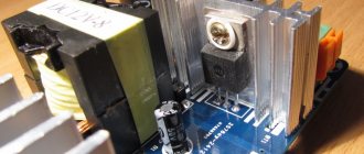
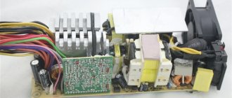
Improving a computer power supply
Our smaller friends (the Chinese) have flooded the electronics market, but they are not always conscientious, but many expensive models of computer power supplies are decent in their class. But still, most power supplies, as I call them, are castrated, that is, when the printed circuit board was designed for some elements, and others are soldered into it, and not all of them, especially for input filters, they are almost never found in cheap models.
ATX block diagram
The main disadvantage of all cheap power supplies
+5V voltage oscillogram of a cheap power supply.
Input EMI filters
Input and output filters are a necessary component of almost any electronic system that includes switching converters or high-speed components.
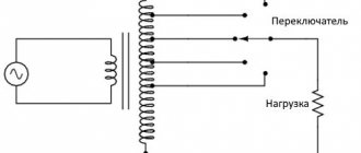
Although input EMI filters and output anti-aliasing filters serve different purposes, their configuration can be similar in some cases. The main purpose of input filters is to protect against electromagnetic interference (EMI) generated by the converter, as well as protection against possible interference from the network. In many cases, the best choice is a commercial EMI filter that provides differential and common mode filtering. These filters are installed between the mains supply and the AC/DC converter. The filters include magnetically coupled chokes and tanks. In the general case, the circuit of such a filter is shown in Fig. 1.
Rice. 1. Common mode and differential EMI filter circuit
In this EMI filter, two filters are connected in series. The near-line EMI differential noise filter consists of capacitors CY5, CY6, CX2 and a magnetically coupled two-winding LDM inductor. An EMI differential noise filter is installed in series with it, which includes capacitors CY3, CY4, CX1 and a magnetically coupled two-winding inductor LCM.
As can be seen from the figure, EMI filters for common-mode and differential noise have a similar configuration, with the exception of the location of the beginning and end of the windings of the LDM and LCM chokes. The difference is explained as follows. Differential noise currents in phase and neutral flow in different directions, and common mode noise currents in phase and neutral flow in one direction and are closed through the frame or ground. Thus, in both chokes the magnetic fluxes created by the two windings add up. Consequently, the inductance of the inductor increases and the EMI filter works like a classic LC filter.
The EMI filters described above are usually installed in 220 V mains voltage lines at the input of the AC/DC converter. EMF filters are produced by many well-known companies in the Russian electronics market, including Murata, Epcos, Würth Elektronik and many others.
The author strongly recommends using purchased filters and not trying to make them yourself from discrete components. EMI filters should not be used on AC circuits in DC circuits. Direct current will create bias in the filter chokes, and surges of interference currents lead to saturation of the inductor core, which entails a decrease in their inductance and, consequently, filtering properties.
However, it is not always possible to use ready-made EMI filters. For example, in distributed power systems in DC circuits after or before the bus converter, it may be necessary to install an EMI filter before the PoL converter. In this case, you will most likely have to create such a filter using discrete components, especially if the power of the converter in front of which the filter is installed is low.
An example is the LC filter shown in Fig. 2. Since the filter is described by a 2nd order equation and is a well-known oscillatory element, we will only present the final relations.
Rice. 2. LC-type EMI filter
The natural frequency of the oscillatory link is determined from relation (1):
ω0 = 1/√LC. (1)
The amount of damping is determined from relation (2):
β = (R/2) × (√C/L). (2)
In the diagram in Fig. 2 there is no resistor R in explicit form, therefore such a filter is called undamped, but this does not mean that R = 0 and any input influence generates undamped oscillations in the filter. The value of R is the sum of the ohmic resistance of the inductor RDC, the equivalent series resistance of the capacitor (ESR) and the resistance of the conductors. The transfer characteristic of this filter is shown in Fig. 3.
Rice. 3. Transfer characteristic of LC filter
As can be seen from this figure, the lower the damping degree β, the more pronounced the resonant peak in the frequency domain. Also, under the condition β<1, the smaller β, the more pronounced the oscillatory transient process in the time domain. In the latter case, the aphorism “the best is the enemy of the good” is quite appropriate. There are known cases where, due to the use of high-quality capacitors with very low ESR in DC buses, voltage fluctuations on the bus occurred precisely because of the low ESR value, since as ESR decreased, the degree of damping decreased and the oscillation of the transient process increased.
One more circumstance should be taken into account: the EMI filter will work as designed only if its output impedance is significantly less than the input impedance of the converter. Otherwise, connecting the converter to the filter output will noticeably distort the filter characteristics. And the filter can distort the operation of the converter.
In general, the input circuit of the converter can be represented as a sequential RLC chain. Thus, the frequency characteristic of the impedance will have an extremum in the form of a minimum. To eliminate the mutual influence of the EMI filter and the converter, it is desirable that the output impedance of the converter be an order of magnitude less than the input impedance of the EMI filter.
In Fig. Figure 4 shows an example of the frequency dependence of the impedances of the EMI filter and converter. From this figure, as well as from the above considerations, it is clear that the damping amount should not be too small. On the other hand, an excessive increase in β will eliminate oscillations, the transition process will become aperiodic and drag on over time. As a rule, the optimal β value should be selected between 0.5 and 1.0.
Rice. 4. Frequency dependences of the impedances of the EMI filter and converter
With an undamped filter (Fig. 2), the value of R in relation (2) is mainly determined by the sum of RDC + ESR, but this value is not enough to increase β to 0.7–1.0. Therefore, additional resistance must be introduced. The best option for introducing a damping chain is shown in Fig. 5. Chain Z3 consists of a resistor Rd and a capacitor Cd connected in series. The latter blocks the DC voltage and prevents additional power loss across the resistor Rd. The damping coefficient of an EMI filter with a damping chain is described by expression (3):
βd = (n/n + 1) [(Rd/2) × (√C/L)], (3)
where n = Cd/C.
Rice. 5. Damped LC filter
For practical reasons, the value of n should be in the range of 4–7 units. In Fig. Figure 6 shows the frequency dependence of the impedances of the damped and undamped filters. The resonant peak of a damped EMI filter is significantly smaller than that of an undamped one. The damping circuit can be composed of a series RL circuit and connected in parallel to the filter inductance, but this is not the best solution, in our opinion, since the power dissipation on the resistor increases.
Rice. 6. Frequency dependences of the impedances of the damped and undamped LC filter
If you turn on several LC filters in series, the slope of the frequency response of the EMI filter in the region ω>ω0 will increase, and noise filtering will improve, but, as it seems to the author, such a solution does not make sense. The dimensions of the solution will increase noticeably, and increasing the slope of the filter's frequency response will not bring practical benefits. The operating frequency of PoL converters is currently in the range of approximately 1–2 MHz.
Taking into account the requirements of the standards, the cutoff frequency of the EMI filter must be within a few kHz. If you choose a value β ≈ 1, then the attenuation at a frequency of 1 MHz will be 50–60 dB, which is quite sufficient to suppress interference. If more significant attenuation is still required, you may not want to consider using a two-stage EMI filter, but rather analyze the power supply and take other measures to reduce interference.
Device
If we talk about the design of such a thing as a surge protector, then it should be said that it can belong to one of 2 categories:
- stationary-multichannel;
- built-in
In general, the circuit of a conventional surge protector designed for a voltage of 220 V will be standard and, depending on the type of device, may differ only slightly.
If we talk about built-in models, their peculiarity is that the contact boards of such filters will be part of the internal structure of electronic equipment.
Other equipment also has such boards, which falls into the category of complex ones. Such boards usually consist of the following components:
- additional type capacitors;
- induction coils;
- toroidal type throttle;
- varistor;
- thermal type fuse;
- VHF capacitor.
A varistor is a resistor that has variable resistance. If the standard voltage threshold of 280 volts is exceeded, then its resistance decreases. Moreover, it can decrease by more than ten times. A varistor is essentially a surge protector. And stationary models usually differ in that they have several outlets. Thanks to this, it becomes possible to connect several models of electrical equipment to the electrical network through a surge protector.
In addition, all surge protectors are equipped with LC filters. Such solutions are used for audio equipment. That is, such a filter is noise suppressing, which will be extremely important for audio and working with it. Also, surge protectors are sometimes equipped with thermal fuses, which help prevent voltage surges. Sometimes some models use disposable fuses.
Output smoothing filters
The same LC filters that were discussed above are used as smoothing output filters. However, in this case, such filters cannot be replaced with purchased ones, and the developer has to calculate them each time. The output smoothing filter allows you to reduce output voltage ripple to units of mV or even several hundred μV. Reducing the ripple amplitude to tens of µV is hardly possible, even if the number of output filter stages is increased.
The parasitic components of the filter components and the conductors of the printed circuit board will interfere with the reduction of ripple. In addition, due to switching frequency jitter, low-frequency components down to several Hz may appear in the output voltage spectrum. They, of course, cannot be suppressed by an anti-aliasing filter. Thus, if it is necessary to limit the output voltage ripple down to µV, an LDO regulator is installed in the power circuit after the smoothing filter.
Rice. 7. Anti-aliasing filter at the output of the boost converter
Let's consider the most common anti-aliasing filter configuration - the π-filter (or P-filter). The diagram of its connection to the boost converter circuit is shown in Fig. 7 [1]. The resonant frequency of this filter is determined from expression (4).
Unlike the EMI filter, the anti-aliasing filter is part of the feedback loop, so the cutoff frequency of the filter should not be less than 10–20% of the switching frequency. Otherwise, the stability of the system decreases due to a delay in the feedback loop, which leads to prolongation of transient processes, as well as to deterioration of stability due to a decrease in the phase margin. As with EMI filters, a damping circuit must be included in the anti-aliasing filter. In Fig. Figure 7 shows three possible options for damping chains.
Damping option 1 with the introduction of the RFILT resistor seems to be the simplest and most economical, but the introduction of this resistor weakens the effectiveness of the filter. In addition, the impedance of the parallel RL filter circuit is reduced. Damping option 2 is the most effective because this circuit improves the filter performance, but increases the cost due to the use of a ceramic capacitor. At first glance, it may seem that damping option 3 is the most effective. However, in this case the largest capacitor capacity is required. Consequently, the cost of the solution increases. In addition, since introducing this chain will reduce the feedback loop bandwidth, this option should be excluded from consideration.
For high-frequency converters with low output current, there is another non-trivial version of the smoothing filter - instead of a choke, a resistor is used in the filter. Let's consider a simple example where an RC filter is used as the output filter of a PoL converter with a switching frequency of 2 MHz and an output current of 20 mA. Let the resistor be 10 ohms and the capacitor be 1 µF. The cutoff frequency of this filter will be about 16 kHz; Taking into account the attenuation of 20 dB/decade, we find that ripples with a frequency of 2 MHz are attenuated by more than 100 times. However, you will have to put up with a voltage drop of 200 mV across the resistor.
Note that the calculation of filters is approximate and the calculated parameters must be checked by prototyping the filter together with the converter. The value of the filter capacitance is affected by the charge voltage, current pulsation frequency, and capacitance temperature. The inductance of the filter choke depends nonlinearly on the current. In addition, the converter will also affect the filter characteristics. These changes cannot be taken into account in practical calculations. Assistance in filter development is provided by proprietary CAD systems for calculating filters. For example, a scheme for calculating an anti-aliasing filter can be found in [1]. To calculate the EMI filter, you can use the tools of [2].
Step response
The output voltage must remain stable when the voltage at the input of the pulse converter changes.
Likewise, if the output current suddenly decreases or increases, the output voltage must be quickly adjusted. Figure 10 shows the transient response of a variable stability switching controller (yellow curve) with an output voltage of 5 V when the load current suddenly changes from 0 to 1 A (green curve). Rice. 10. Transient response of a stable pulse controller
When the load current suddenly changes, the control circuit must quickly adjust the output voltage to the specified level. The output voltage should not change significantly as a result of the surge response, otherwise electronic circuits may be damaged due to overvoltage. Ideally, after a load surge, the output voltage is quickly adjusted to the set value; there are no emissions or even ringing. Ringing at the compensation stage is due to unstable operation of the pulse converter. The operation of a pulsed power supply controller is considered stable if it responds quickly enough to abrupt changes in the load and promptly compensates for this change.
conclusions
So, if the output filter is installed in the control loop, its characteristic equation is 2nd order or higher, depending on the type of filter.
The compensation circuit must have no less order, which leads to an increase in the inertia of the control circuit. Therefore, it is not recommended to include an output filter in the control loop. The output voltage of the converter should be removed before the output filter. It is also advisable to select filter chokes and ferrites with the lowest RDC resistance to reduce losses in the output filter. Technical support