In everyday life, a powerful power source with a fixed voltage is often needed. It can be used as a charger, to power audio equipment (amplifiers), etc. It is advisable to make such power supplies using a pulse circuit. This circuitry allows you to create lightweight and powerful DC voltage sources. The complexity of the circuit begins to fade into the background compared to its advantages already at load currents of more than 2A. You can make a switching power supply with your own hands if you have the equipment and certain qualifications.
Types and principle of operation of switching power supplies
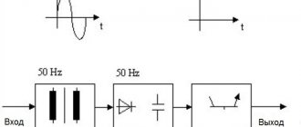
The basic operating principle of a switching power supply (SMPS) is that direct voltage (rectified mains voltage or from a third-party source) is converted into pulsed voltage with a frequency of up to hundreds of kilohertz. Due to this, the winding parts (transformers, chokes) are light and compact.
Fundamentally, IIPs are divided into two categories:
- with pulse transformer;
- with storage inductance (it can also have secondary windings)
The former are similar to conventional transformer mains power supplies; their output voltage is regulated by changing the average current through the transformer winding. The latter work on a different principle - they are regulated by changing the amount of accumulated energy.
Based on other characteristics, IIP can be divided into unstabilized and stabilized, unipolar and bipolar, etc. These features are not of such a fundamental nature.
Frame
It is very convenient to make the housing for the power supply from aluminum. First, a frame is assembled from corners, which is then sheathed with aluminum plates. There are at least two advantages of this solution - firstly, aluminum is easy to work with, and secondly, it conducts heat very well, which will protect the power supply from overheating.
Structural and schematic diagram of the main parts of the block
Generalized block diagram of a pulse power supply.
A surge filter is installed at the input of the power supply. In principle, it does not affect the operation of a homemade or industrial switching power supply - everything will function without it. But you cannot abandon the filtering circuit - due to the extremely nonlinear shape of the consumed current, pulsed sources intensively “sprinkle” interference into a 220-volt household network. For this reason, devices running on the same network on microprocessors and microcontrollers - from electronic watches to computers - will malfunction.
Network filter circuit.
The purpose of the input device is to protect against two types of interference:
- common-mode (asymmetrical) – occurs between any wire and the ground (case) of the power supply unit;
- differential (symmetrical) – between the power wires (poles).
The filter, like the entire power supply, is protected at the input by fuse F (fuseable or self-recovering). After the fuse there is a varistor - a resistor whose resistance depends on the applied voltage. As long as the input voltage is normal, the resistance of the varistor is high and it has no effect on the operation of the circuit. If the voltage increases, the resistance of the varistor drops sharply, which causes an increase in current and the fuse burns.
Capacitors Cx block differential noise at the input and output of the filter in the range up to 30 MHz. At a frequency of 50 Hz their resistance is high, so they do not affect the mains voltage. Their capacitance can be selected from 10 to 330 nF. Resistor Rd is installed for safety - the capacitors are discharged through it after the power is turned off.
Common-mode interference is suppressed by a filter on Cy and L. Their values for the cutoff frequency f are related by the Thompson formula:
f=1/(2*π*√L*C) , where:
- f – cutoff frequency in kHz (the conversion frequency of the pulse generator is taken);
- L – inductance of the inductor, μH;
- C – capacitance Cy, µF.
The common mode choke is wound on a ferrite ring. The windings are identical, winding on opposite sides.
Common mode choke design.
Unlike the output filter, the rated current of the power supply unit does not affect the calculation of the noise protection filter elements, with the exception of the wire with which the inductor is wound.
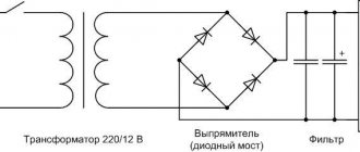
After the filter, the mains voltage is rectified. In most cases, a standard full-wave bridge rectifier is used.
Mock Tests
Before starting to build a working structure, you should test everything on the knees, make sure that the screwdriver is operating stable under load and that there is no severe overheating in the power supply.
We take the computer power supply and check it: plug it into the network, find green in the output bundle of wires (they say it can be a different color, but I always came across green ones) and connect it with a jumper to any of the black ones (all black wires at the output are the common output, in our case it is a minus). The unit should turn on and a voltage of 12 volts will appear between the black and yellow wires. You can check this with a multimeter or by connecting any computer cooler to the named terminals.
If everything is in order and the unit produces about 12 volts on the yellow (+) and black (-) terminals, continue. If there is no voltage at the output, we look for another unit or repair this one; this separate topic will be described separately.
We cut off the plug from the output of the block and take 3-4 yellow and black wires coming from the block and connect them in parallel. When cutting off the plug, do not forget about the green starting conductor, it must be shorted to black. We received a 12 V source with a decent current load capacity of 10-20 A, the currents depend on the model and power of the unit.
Now we need to connect our 12 V to the terminals of the screwdriver without a battery; we look at the polarity of the connection using the battery. Well, we check the screwdriver - at idle speed, then slowing down by hand. At this stage, I encountered a problem: when I press the button fully, the screwdriver works, but when I slowly, smoothly press the screwdriver button, the power supply goes into protection. To reset the protection, you must disconnect the unit from the network and turn it on again. This won’t work at all, we need to somehow correct this instability.
I pulled the block board out of the case and additionally hooked up a multimeter to constantly monitor the voltage
In my opinion, this phenomenon may occur due to the fact that the power supply and the screwdriver button are controlled by PWM controllers; due to interference along the power wires, the controllers somehow interfere with each other. We are trying to solve this problem using an improvised LC filter.
I assembled the filter in 5 minutes from what was at hand: 3 electrolytic capacitors of 1000 uF at 16 volts, a non-polar capacitor of less than 1 uF and wound 20 turns of copper wire with a diameter of 2 mm on a ferrite ring from another unit. Here is his diagram:
And this is what he looks like. This is a purely trial version, in the future this design will be transferred to the battery housing of the screwdriver and will be made more accurately.
We check the entire structure: the block does not go into protection in any position of the button, great! Now you can try tightening several screws - all in a bunch. It seems that the screwdriver will be able to tighten larger screws.
Well, now you need to remove all the snot and piles of wires, remove the “dead cans” from the battery case, replace them with an LC filter, and test the screwdriver in more realistic conditions.
Inverter circuits
The resulting rectified voltage is supplied to the converter (inverter). It is performed on bipolar or field-effect transistors, as well as on IGBT elements that combine the properties of field-effect and bipolar ones. In recent years, high-power, low-cost insulated gate field-effect transistors (MOSFETs) have become widespread. It is convenient to build key inverter circuits on such elements. Switching power supply circuits use various options for connecting MOSFETs, but push-pull circuits are mainly used due to their simplicity and the ability to increase power without significant modifications.
Push-pull scheme
Push-pull converter circuit.
A push-pull inverter (push - push, pull - pull) is an example of a push-pull converter. Transistor switches operate on the primary winding of the transformer, consisting of two half-windings I and II. The transistors open alternately for a given period of time. When the top transistor in the circuit is open, current flows through half-winding I (red arrow), when the second one flows through half-winding II (green). To avoid a situation where both switches are open (due to the finite speed of the transistors), the control circuit creates a pause called Dead time.
Transistor control taking into account Dead time.
This circuit works well at low supply voltage (up to +12 volts). The downside is the presence of surges with an amplitude equal to twice the supply voltage. This entails the use of transistors designed for twice the voltage.
Bridge circuit
The push-pull bridge is free from the main drawback of the previous scheme.
Push-pull bridge inverter circuit.
Here, a pair of transistors T1 and T4 , then T2 and T3 (the key control signal is generated taking into account Dead time). In this case, the primary winding is connected to the power source first on one side, then on the other. The pulse amplitude is equal to the full supply voltage, and there are no voltage surges. The disadvantages include the use of four transistors instead of two. In addition to increasing the size of the power supply, this leads to doubled voltage losses.
Half bridge circuit
In practice, a half-bridge inverter circuit is often used - to a certain extent, a compromise between the previous two circuits.
Half-bridge circuit.
In this case, one side of the winding is switched by alternately opening transistors T1 and T2, and the other is connected to the midpoint of the capacitive divider C1, C2. Advantages of the scheme:
- unlike push-pull, there are no voltage surges;
- unlike bridge, only two transistors are used.
On the other side of the scale, the transformer winding is powered by only half the supply voltage.
Single-ended circuits
In the circuitry of converters, single-cycle circuits are also used - forward and flyback. Their fundamental difference from push-pull ones is that the transformer (more precisely, its primary winding) simultaneously serves as a storage inductance. In flyback circuits, energy is accumulated in the primary winding during the open state of the transistor, and is transferred to the load through the secondary winding during the closed state. In direct thrusters, energy accumulation and release to the consumer occur simultaneously.
Two phases of operation of a flyback single-cycle inverter.
⇡#What power is needed for modern gaming PCs
Let me note again: this article is to a certain extent tied to the “Computer of the Month” section. Therefore, if you are visiting us for the first time, I recommend that you at least read the August issue. Each “Computer of the Month” covers six assemblies, mostly gaming ones. I used similar systems for this article. Let's get acquainted:
- The combination of Ryzen 5 1600 + Radeon RX 570 + 16 GB of RAM is an analogue of the starting assembly (35,000-37,000 rubles per system unit, excluding the cost of software).
- The combination of Ryzen 5 2600X + GeForce GTX 1660 + 16 GB of RAM is an analogue of the basic assembly (50,000-55,000 rubles).
- A combination of Core i5-9500F + GeForce RTX 2060 + 16 GB of RAM is an analogue of the optimal assembly (70,000-75,000 rubles).
- A combination of Core i5-9600K + GeForce RTX 2060 + 16 GB of RAM is another optimal build option.
- A combination of Ryzen 7 2700X + GeForce RTX 2070 + 16 GB of RAM is an analogue of an advanced build (100,000 rubles).
- The Ryzen 7 2700X + Radeon VII + 32 GB RAM combination is similar to the maximum build (130,000-140,000 rubles).
- A combination of Core i7-9700K + Radeon VII + 32 GB of RAM is another option for the maximum build.
- A combination of Core i9-9900K + GeForce RTX 2080 Ti + 32 GB of RAM is an analogue of an extreme build (220,000-235,000 rubles).
Unfortunately, I was not able to get Ryzen 3000 processors at the time of conducting all the tests, but the results obtained will not become less useful. The same Ryzen 9 3900X consumes less than the Core i9-9900K - it turns out that within the framework of an extreme build, studying the power consumption of an 8-core Intel processor will be even more interesting and important.
And also, as you may have noticed, the article uses only mainstream platforms, namely AMD AM4 and Intel LGA1151-v2. I did not use HEDT systems such as TR4 and LGA2066. Firstly, we abandoned them in the “Computer of the Month” a long time ago. Secondly, with the advent of the 12-core Ryzen 9 3900X in the mass segment and in anticipation of the imminent release of the 16-core Ryzen 9 3950X, such systems have become extremely highly specialized. Thirdly, because the Core i9-9900K still gives everyone a run for their money in terms of power consumption, once again proving that the calculated thermal power declared by the manufacturer tells the consumer little.
Now let's move on to the test results.
To be honest, I present the results of testing in programs such as Prime95 and Adobe Premier Pro 2022 more for information purposes - for those who do not play or use discrete video cards. You can safely rely on these data. Basically, here we are interested in the behavior of test systems under loads close to maximum.
And here some very interesting things are observed. In general, we see that all the systems considered do not consume very much energy. The most voracious, which is quite logical, was the system with Core i9-9900K and GeForce RTX 2080 Ti, but even it in stock (read - without overclocking) consumes 338 W when it comes to games, and 468 W at maximum PC load. It turns out that such a system will have enough power supply for an honest 500 W. It is so?
Power transformer
The power transformer operates at high frequencies (up to several tens of kilohertz), so it can be made on a core made of ferrite rather than transformer iron. Also, due to the increased frequency, its dimensions will be smaller than that of a network one, designed for conversion at a frequency of 50 Hz. The calculation of a pulse transformer is quite extensive. You can understand it for general development, but for practical purposes it is better to use some program, including online services.
Interface of the Lite-CalcIT program.
The Lite-CalcIT program is popular. She can calculate a transformer for an existing core, or she can select the optimal one based on the entered data.
Components of the device
The mechanism we are assembling today consists of three parts:
step-down transformer, which is the most important and integral part; a capacitor, with the help of which the current voltage is stabilized to optimal readings; diodes that are necessary to assemble a diode bridge with your own hands.
Each part is very important. If an error is made in any of them during assembly, this will lead to the fact that the assembled unit and the household electrical appliance connected to the system will not work correctly. And also the assembled device may not turn on at all. Let's look at each of the components of the mechanism in more detail.
Snubber
To compensate for current and voltage surges that inevitably arise when switching the primary winding of a transformer, damper circuits are used, called snubbers in English technical literature. Such circuits can be installed along the power supply (parallel to the primary winding of the transformer) or separately on each switch. The design of snubbers can be different, but the most widespread are dampers in the form of a sequential RC chain (diagram b in the figure).
Various damper schemes.
There is no substantiated method for calculating a snubber. To do this, it is necessary to take into account all parasitic inductances (windings, tracks, capacitors) at many frequencies and for unknown wave impedances. Therefore, all existing calculations are empirical in nature.
The main (and only) active element of the damper is the capacitor. It “absorbs” impulse emissions. The resistor only worsens the damping properties, but limits the current through the capacitor, which can reach significant values, albeit for a short time. This scheme is more relevant in thyristor converters.
You can find out what a snubber or damper is by watching the video.
The RCD snubber circuits (c and d in the figure) contain diodes. They can be useful for limiting reverse polarity pulses in thyristor and bipolar transistor circuits. If the switches are assembled on field-effect or IGBT transistors, then there is no point in installing valves - they duplicate the diodes present inside these transistors.
The capacitance of the capacitor is selected in the range of 0.1–0.33 μF. In 90+ percent of cases this is enough. An increase or decrease in value is used for keys operating under non-standard conditions (increased conversion frequency, etc.)
Rectifier
The voltage of the secondary winding must be rectified. For levels up to 12 volts, it is advisable to use a full-wave, midpoint circuit.
Diagram of a rectifier with a midpoint and the passage of current through it.
The advantage of this circuit is that the current flows in each direction through only one diode, and the voltage drop across the valves, in contrast to the classic bridge circuit, is half as much. This can significantly reduce the required number of turns of the secondary winding. The same purpose is served by the use of Schottky diodes and assemblies of them.
Bridge rectifier circuit and current flow through it.
If the output voltage of the power supply is higher than +12 volts, then saving 0.6 volts becomes insignificant, and you can make a rectifier according to the standard circuit and use a transformer without a tap.
If the output of a switching power supply must be bipolar, tapping from the midpoint again becomes rational. In this case, 4 diodes and radiators for them are saved at once - the gain in size can be significant.
Bipolar rectifier with midpoint.
Filter
The output voltage must be filtered - it contains a large number of conversion products. Since the inverter operates at a fairly high frequency, filters containing not only capacitors, but also small-sized chokes with relatively low inductance become effective.
L- and U-shaped LC filters.
To calculate the filter elements, it is necessary to specify the pulsation coefficient Kp. It is selected from the expected load:
- sensitive equipment for radio reception, preliminary stages of audio equipment, microphone amplifiers - Kp = 10-5..10-4 ;
- audio frequency amplifiers – Кп=10-4..10-3 ;
- middle and low class receiving and sound reproducing equipment – Kp=10-2..10-3 .
For an L-shaped filter installed after a full-wave rectifier, the following relations apply:
- L*C=25000/(f2+Kp);
- L/C=1000/R2н.
In these formulas:
- L – inductance of the inductor in µH;
- C is the capacitance of the capacitor in microfarads;
- f – conversion frequency in Hz;
- Rн – load resistance in Ohms.
For U-shaped filter:
- С1=С2=С;
- L/C=1176/R2н.
The dimension of the values is the same as for the previous filter.
Circuits and manufacturing of switching power supplies
Switching power supplies are assembled on various element bases. Typically, specialized microcircuits specially designed for creating such devices are used to build SMPS. Except for the simplest blocks.
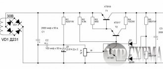
Powerful pulse unit on ir2153
Simple power supplies can be built on the IR2153 chip. It is a powerful integrated driver with a timer similar to the NE555. The generation frequency is set by external elements. The microcircuit does not have inputs for organizing feedback, so current and voltage stabilization cannot be obtained using the PWM method.
Pin layout of the IR2153 chip.
The assignment of the pins is given in the table.
| № | Designation | Purpose | Purpose | Designation | № |
| 1 | Vcc | Power supply for logic and drivers | Power output switches | Vb | 8 |
| 2 | Rt | Frequency setting resistor | Top Driver Output | HO | 7 |
| 3 | Ct | Frequency setting capacitor | Top Driver Power Return | Vs | 6 |
| 4 | COM | General | Bottom Driver Output | L.O. | 5 |
Internal circuit of IR2153.
To better understand the operation and pin assignments, it is best to study the internal circuitry. The main point that you need to pay attention to is that the output switches are assembled using a half-bridge circuit.
Using this chip you can assemble a simple power supply.
Scheme of a simple power supply based on IR2153.
The IR2153 is powered by 220 volts through a quenching resistor R1, a diode rectifier VD3, and a filter on C4. The generation frequency is set by elements C5, R2 (with the values indicated in the diagram, it turns out to be about 47 kHz). A transformer can be considered a program. The author's version used a power transformer from a computer power supply. The standard windings have been removed, the primary is wound into two cores with enamel insulated wire with a diameter of 0.6 mm.