Many amateur radio designs use switching power supplies (PS). They are small in size with significant power. This reduction was made possible due to the high frequency. At such frequencies, you can get a high output voltage with a small number of turns. For example, to obtain a voltage of 12 V at a current of 1 A, you need to wind only five turns. In addition, switching power supplies have a high efficiency, since the losses on the transformer are very small.
These power supplies also have disadvantages: they create high-frequency interference and impose high load requirements. The latter should not be more or less than that for which the power supply is designed.
Theory of switching power supplies
In conventional power supplies, voltage variation and galvanic isolation were performed on a steel-core transformer operating at 50 Hz, a solid-state rectifier, and a linear voltage regulator.
However, the efficiency of this circuit is very low (does not exceed 50%), most of the power is converted into heat in the transformer, diode and analog stabilizer. Large rated output power requires a larger mains transformer and high heat loss. This inconvenience can be avoided by increasing the operating frequency to several hundred kHz and replacing the voltage regulator with an electronic key with intelligent control. Their task is to convert the mains voltage into direct voltage, and then into rectified voltage, carried out by quickly switching transistors. The result is a high-frequency square-wave voltage, which is converted by a pulse transformer and a rectifier.
Stabilization of the output power is achieved by changing the pulse width at a constant frequency or by switching at certain periods of time depending on the load of the circuit. The most important advantages of SMPS, comparable to conventional power supplies:
- light weight, reduced volume, increased efficiency
- low capacitance filter capacitors for high switching frequencies
- no audible interference due to the switching frequency being outside the audible range
- easy control of different output voltages
- Easily reduce high mains voltage
With the development of high-power fast-switching transistors for high frequencies, it has become possible to use SMPS operating at frequencies up to 1 MHz. With this type of resonant transformer, operating frequencies can be increased even to 3 MHz. However, these benefits are diminished by unwanted high-frequency emissions as well as slower response times to possible load changes.
However, the availability of new magnetic materials for transformers operating in the frequency range up to about 1 MHz, as well as advances in power supplies, have stimulated the development of new high-frequency transformer cores.
This trend has led to the development of new Mn-Zn ferrites with very fine grain structures and materials with reduced hysteresis losses, allowing power transmission in the 1 to 3 MHz range. High operating frequencies lead to a further reduction in the size of the cores and, consequently, the entire power supply. The new design principle in planar technology makes it possible to produce high-frequency transformers with radically reduced dimensions (planar transformers, low-profile transformers). This technology has a strong impact on the development of AC/DC converters, as well as the production of hybrid switching power supplies.
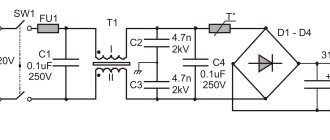
But let's get back to theory. A switching power supply works by controlling the average voltage supplied to the load. This is done by opening and closing a switch (usually a high-power field-effect transistor) at a high frequency. The system is better known as pulse width modulation - PWM. The PWM circuit is the most important one that distinguishes this type of power supply, so it’s worth remembering at least the name itself.
The diagram below shows the ideas behind PWM operation and is quite simple to understand: V = voltage, T = period, t (on) = pulse width. The average voltage applied to the load can be explained by the following formula:
Vo(av) = (t(on)/T) x Vi
The pulses follow each other quickly (this is on the order of many kHz, that is, thousands of times per second), and in order for the load not to see sudden pulses, capacitors are needed to provide a relatively constant voltage level. A decrease in time t (on) causes a decrease in the average value of the output voltage Vo (av) and vice versa - an increase in the duration of the high voltage state t (on) increases the output voltage Vo (av).
Let's assume that a switching power supply supplies +12V to a 6A load. Now, when the load current suddenly rises to 8A, the voltage automatically drops to +10.6V. In a fraction of a second, the feedback sent to the PWM circuit will notice the drop voltage and turns on the MOSFET for a longer period of time t (on). Thanks to this, the circuit can transfer more power and restore the output voltage to +12 V.
The frequency at which PWM operates is typically in the range of 30 kHz to 150 kHz, but can be much higher.
Power transformer
The power transformer operates at high frequencies (up to several tens of kilohertz), so it can be made on a core made of ferrite rather than transformer iron. Also, due to the increased frequency, its dimensions will be smaller than that of a network one, designed for conversion at a frequency of 50 Hz. The calculation of a pulse transformer is quite extensive. You can understand it for general development, but for practical purposes it is better to use some program, including online services.
Interface of the Lite-CalcIT program.
The Lite-CalcIT program is popular. She can calculate a transformer for an existing core, or she can select the optimal one based on the entered data.
The principle of operation of the SMPS and its design
A switching power supply is a device that operates on the principle of an inverter, that is, it first converts alternating voltage into direct voltage, and then again converts it into an alternating voltage of the desired frequency. Ultimately, the last stage of the converter is still based on voltage rectification, since most devices still operate at a reduced DC voltage. The essence of reducing the size of these power supply and converting devices is based on the operation of the transformer.
The fact is that the transformer cannot operate with constant voltage. Simply, an EMF (electromotive force) will not be induced at the output of the secondary winding when direct current is supplied to the primary. In order for voltage to appear on the secondary winding, it must change in direction or magnitude. Alternating voltage has this property; the current in it changes its direction and magnitude with a frequency of 50 Hz. However, in order to reduce the size of the power supply itself and, accordingly, the transformer, which is the basis of galvanic isolation, it is necessary to increase the frequency of the input voltage.
At the same time, pulse transformers, unlike conventional linear ones, have a ferrite core of the magnetic circuit, and not a steel core made of plates. And also modern power supplies working on this principle consist of:
- mains voltage rectifier;
- a pulse generator operating on the basis of PWM (pulse width modulation) or a Schmitt trigger;
- DC stabilized voltage converter.
After the mains voltage rectifier, a pulse generator using PWM generates it into alternating voltage with a frequency of about 20–80 kHz. It is this increase from 50 Hz to tens of kHz that makes it possible to significantly reduce both the dimensions and weight of the power source. The upper range could be larger, however, then the device will create high-frequency interference, which will affect the operation of radio frequency equipment. When choosing PWM stabilization, it is imperative to also take into account the higher harmonics of the currents.
Even when operating at these frequencies, these pulsed devices produce high-frequency noise. And the more of them in one room or in one enclosed space, the more of them there are in radio frequencies. To absorb these negative influences and interference, special noise suppression filters are installed at the input of the device and at its output.
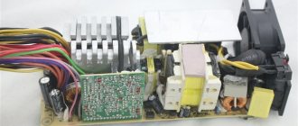
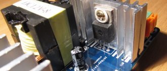
This is a clear example of a modern switching power supply used in personal computers.
A - input rectifier. Half-bridge and full-bridge circuits can be used. Below is an input filter having inductance; B - input smoothing capacitors with a fairly large capacitance. To the right is a heatsink for high-voltage transistors; C - pulse transformer. A radiator for low-voltage diodes is mounted to the right; D - output filter coil, that is, group stabilization choke; E - output filter capacitors. The coil and large yellow capacitor below E are components of an additional input filter mounted directly on the power connector, and not part of the main circuit board.
If a radio amateur invents a circuit himself, he must look into the reference book on radio components. The reference book is the main source of information in this case.
We recommend reading: What is a voltage divider and where is it used?
How does an inverter work?
RF modulation can be done in three ways:
- pulse-frequency;
- phase-pulse;
- pulse width.
In practice, the last option is used. This is due both to the simplicity of implementation and to the fact that PWM has a constant communication frequency, unlike the other two modulation methods. A block diagram describing the operation of the controller is shown below.
Block diagram of a PWM controller and oscillograms of the main signals
The operating algorithm of the device is as follows:
The reference frequency generator generates a series of rectangular signals, the frequency of which corresponds to the reference one. Based on this signal, a sawtooth UP is formed, which is supplied to the input of the PWM comparator. The signal UUS coming from the control amplifier is supplied to the second input of this device. The signal generated by this amplifier corresponds to the proportional difference between UП (reference voltage) and UРС (control signal from the feedback circuit). That is, the control signal UUS is, in fact, a mismatch voltage with a level that depends on both the current across the load and the voltage across it (UOUT).
This implementation method allows you to organize a closed circuit that allows you to control the output voltage, that is, in fact, we are talking about a linear-discrete functional unit. Pulses are generated at its output, with a duration depending on the difference between the reference and control signals. Based on it, a voltage is created to control the key transistor of the inverter.
The process of stabilizing the output voltage is carried out by monitoring its level; when it changes, the voltage of the control signal UPC changes proportionally, which leads to an increase or decrease in the duration between pulses.
As a result, the power of the secondary circuits changes, which ensures stabilization of the output voltage.
To ensure safety, galvanic isolation between the power supply and feedback is necessary. As a rule, optocouplers are used for this purpose.
Difference from transformer
It’s easy to understand how a transformer power supply works:
- The current enters the transformer coil, where, depending on the purpose of the power supply, the voltage increases or decreases, while remaining variable.
- Then comes the diode bridge - converter. Its task is to invert alternating voltage into direct voltage.
- The last block is a capacitor that smoothes the pulses.
There are several disadvantages to such a power supply:
- Larger size. This power supply does not include a stabilizer (except for the output capacitor).
- The stabilization of transformers is extremely doubtful. They miss races more often, which can cause equipment breakdowns.
In switching power supplies, the operating principle is somewhat different: the generator creates its own clock, which stabilizes the voltage. It is possible to use miniature transformers without losing power. Key stabilization elements are used.
LLC Resonant SMPS based on IRS27952 [2018]
In this article we will talk about an LLC resonant switching power supply (SMPS), for UMZCH based on the IRS27952 controller (aka IRS27951), and a simplified method for calculating all elements for this switching power supply will also be described in detail. I would like to immediately draw your attention to the fact that the process of calculating and manufacturing a resonant SMPS is very complex and not everyone can cope with it, so it is not recommended for inexperienced radio amateurs to undertake the construction of this power supply; evaluate your strengths correctly. Of course, to make such a power source, you must have an oscilloscope and a device that allows you to measure capacitance and inductance (LC meter). The calculation method described in the article is simplified; it does not take into account all the nuances and subtleties, but it is enough to build a workable resonant switching power supply. The article will not contain a detailed description of the operating principle of resonant pulse converters; the main emphasis will be on describing the process of calculating and manufacturing a resonant SMPS.
What are the advantages of a resonant SMPS in comparison with a “classical pulse generator”? The advantages of the resonant mode are low losses and electromagnetic interference (which are much easier to control and filter), lower recovery losses of rectifier diodes, less load on all elements of the power supply, which gives increased reliability and durability relative to “classical SMPS”, the ability to work at much higher frequencies without sacrificing efficiency, reliability or cost. And the most important advantage: the resonator is fashionable
Next, I will give some technical characteristics of my copy of a resonant SMPS based on IRS27952:
- Output power (estimated) = 250W
- Output power (maximum tested) = 276W
- Output voltage (range 0W to 276W) = +/- 40V (+/-0.1V)
- Efficiency (at 276W output power) = 92%
Oscillograms of the current shape through the primary winding of the resonant transformer (at different output power values):
The described SMPS has a soft start, protection against short circuits in the load and output voltage stabilization, which precisely maintains the output voltage of the converter at the same level throughout the entire range of output powers. When operating at an output power of up to 200W, there is no noticeable heating of any of the elements of the power supply. Power switches were not installed on the radiator. With an output power of 276W, the switches become barely perceptibly warm, but the primary winding of the transformer is already noticeably starting to warm up. Short circuit protection works properly. When the converter output is shorted, generation stops, the power supply goes into sleep mode and remains in it until the short circuit is eliminated. After eliminating the short circuit, after a certain time, the power supply restarts itself and continues to operate in normal mode.
Circuit diagram of a resonant switching power supply based on IRS27952:
I will not describe in detail the principle of operation of the circuit; I will only dwell on certain points. The initial startup of the converter occurs through a chain of resistors R16, R10, R7 and R6. Further power supply to the controller is provided from the self-supply circuit (R14, C8, VD4, VD7). Zener diode VD2 maintains the controller supply voltage at the same level - 16V. I would like to draw your attention to the fact that the IRS27952, unlike for example the IR2153 and IR2161, does not have a built-in zener diode, so the use of an external zener diode is strictly necessary, otherwise the controller is guaranteed to fail. Capacitors C3 and C5 smooth out ripple and eliminate noise in the IRS27952 power circuit. Resistor chains R1, R2, R3 and R5, R9, R15 are designed to discharge capacitors after turning off the mains power to the converter. Special attention should be paid to the following elements: Rfmin, Rfmax, Rfss, Ct, Css - these are the frequency and time-setting elements of the converter, their ratings must be calculated for your specific tasks, this will be discussed further. Zener diodes VD10 and VD13 are also selected for the output voltage you need: the total stabilization voltage of two zener diodes should be equal to the calculated value of the output voltage of one arm, in this case, to obtain an output voltage of +/-40V, two 20V zener diodes are used. Perhaps this is all that can be said about the circuit; fundamentally, it differs little from any of the pulse converter circuits made on controllers from International Rectifier (now Infineon). It's time to move on to the calculations.
Calculation of a resonant circuit. For the calculation, we need the ResonantSMPS from the All In One package, authored by Starichok. I’ll say right away that the calculation method described below is simplified and an experienced eye will be able to find some omissions in it; this was done intentionally in order to simplify the calculation as much as possible, so that the maximum number of untrained radio amateurs can repeat this resonant SMPS. And so, open the program and enter the initial data:
At the first stage, we enter all the initial data as in the screenshot above (we will correct them later). All you need to choose yourself is the output voltage. In the box opposite “Nominal voltage, V”, enter the voltage you need. For example, if you need a bipolar output voltage +/-40V, then enter 80V (80V=40V+40V). I repeat: it is necessary to select the values of the zener diodes VD10 and VD13, so that their total stabilization voltage is approximately equal to the SMPS output voltage you need (the voltage of one arm). That is, if you need an output voltage of +/-40V, then you need to use two 20V zener diodes, if you need, for example, +/-35V, then a VD10 zener diode of 30V and a VD13 zener diode of 5.1V. We calculate the rated current from the required output power of the power supply and voltage. Let’s say we want to get an SMPS with an output power of 200W, which means we need to divide the desired 200W by the rated voltage, in our case 200W/80V, and we get the rated current = 2.5A - we enter this value in the appropriate program window. We indicate direct drop on the diodes at 1V. If you know the exact value of the voltage drop across the diode, then indicate it, but in any case, you can indicate the direct drop across the diodes is equal to one volt; this will have almost no effect on the accuracy of the calculation, much less on the performance. Next, select the type of straightening - bridge. And enter the desired diameters of the wires with which you will wind the transformer. The diameter of the wire should not be more than 0.5 mm; it is better to use a thinner wire and wind it in several wires. After this, select the appropriate core:
I used an ETD29 core and therefore the footprint on the board is made for this type and size of the core; for any other core the printed circuit board will have to be adjusted. And you need to choose a core so that it matches the overall power and the entire winding fits on its frame. After selecting the core, click the “Calculate” button and see what we got:
You immediately need to set the minimum possible value of the non-magnetic gap, equal to what the program suggests (in my case, 0.67 mm) and press the “calculate” button again. After this, we look at only one line - this is the “capacity of the resonant capacitor”. In order to simplify your life and not waste your time and effort on selecting a non-standard capacitance from several series-parallel connected capacitors, we change the value of the resonant frequency in the corresponding program window, so that the capacitance of the resonant capacitor is equal to some standard capacitance value. In my case, the capacitance of the resonant capacitor turned out to be 28nF, the nearest standard value is 33nF, and we will strive for this value.
When manipulating the resonant frequency, the gap value should always be set to the minimum or very close to the minimum value that the program suggests. I recommend choosing a resonant frequency in the range of 85 - 150 kHz. In my case, the resonant frequency corresponding to a “convenient” resonant capacitance turned out to be 90 kHz. All the most important numbers that you need to remember, write down, screenshot, which will be needed in the future:
You will need the values in the red rectangles when winding the transformer. I would like to draw your attention to the fact that the number of turns of the secondary winding corresponds to the entered output voltage value - 80V. If we want to get a power supply with a bipolar output voltage of +/-40V, we need to wind not one, but two secondary windings, in this case two windings of 12-13 turns each (we divide the resulting 25 turns by two). For further calculations, we need to look at the transfer characteristic (to do this, click on the corresponding button in the upper left corner of the program window):
We remember the values of Fmin and Fmax. For us they are equal: Fmin=54kHz, Fmax=87kHz. We will need these values for further calculations.
Calculation of IRS27952 trim ratings. At the very end of this article you need to download the file NominaliObvyazki.xlsx. To open it you will need Microsoft Excel. We open the file and see the following:
All that remains is to enter our Fmin and Fmax obtained above and get all the ratings of the IRS27952 trim. The only thing we need to select is the capacitance of the capacitors Ct, which sets the value of the dead time. Fortunately, this would require a rather complex calculation, which must be performed based on the parameters of the switches used, but since our calculation is simplified, I recommend simply using Ct capacitors, a capacitor with a capacity of 390-470pF. This capacity and the corresponding dead time will be enough to avoid going into hard switching mode when using most popular keys, such as IRF740, STP10NK60, STF13NM60 and those indicated in the 2SK3568 circuit. The optimal soft start duration is 0.1 sec, you can set a longer duration up to 0.3 sec, it no longer makes sense (with the output capacitance of the SMPS capacitors up to 10000 µF). We enter our Fmin and Fmax and get:
All piping values (except for the capacitance of the soft start capacitor) are automatically rounded to the nearest standard values. Here you can also see the actual values of the minimum, maximum frequencies and soft start frequencies, which will be obtained with the standard piping ratings used. The capacitance of the soft start capacitor is composed of several capacitors, ceramic SMD and electrolytic, for this there is enough space on the printed circuit board. At this point the calculation can be considered complete.
Implementation of a resonant circuit. The resonant circuit includes: a resonant transformer, a resonant capacitance and an additional resonant choke (if necessary). We already know the nominal value of the resonant capacitance. The resonant capacitor must be a film capacitor, type CBB21 or CBB81, CL21 is also allowed (but not recommended). The voltage of the capacitor must be at least 630V, preferably 1000V. This is due to the fact that the maximum permissible voltage on the capacitor depends on the frequency of the current through the capacitor; a 400V capacitor will not last long. And now the most interesting thing is the resonant transformer. To wind it, we have all the necessary initial data. How to wind? There are several options. The first option: wind it like a regular transformer - we wind the primary across the entire width of the frame, then we wind the secondary across the entire width of the frame (or vice versa, first the secondary, then the primary). The second option: wind the secondary over the entire width of the frame, and the primary over half or a third of the width of the frame (or vice versa - the primary over the entire width, and the secondary over half or a third of the width of the frame). And the third option: use sectional winding, when the primary and secondary windings are completely separated. To do this, you will need either a special sectioned frame or you will have to make such a frame yourself, dividing the frame with a plastic partition.
Why is this and what does it give? The first option is the simplest, but provides minimal leakage inductance. The second option is very inconvenient to wind and gives an average leakage inductance. The third option gives the highest and most predictable value of leakage inductance, in addition, the most convenient method for winding. You can choose any of the options. Once you have decided on the winding option and have wound the required number of turns of the primary and secondary windings, you need to change the resulting leakage inductance of the primary winding of the resulting transformer. To do this, you need to assemble a transformer. At this stage, there is no need to glue parts of the core and introduce a gap (the leakage inductance does not depend on the size of the gap, its presence or absence), it is enough to temporarily tighten the core with electrical tape. It is necessary, using soldering, to reliably short-circuit all the terminals of the secondary winding to each other and measure the inductance of the primary winding. The resulting inductance value will be the leakage inductance of the primary winding of the transformer. Let's say you get a leakage inductance of 50 μH. We compare the resulting value with the calculated value of Lr, which you calculated above:
It didn't work out! We need 94 µH, but we got 50 µH. What to do? The main thing is not to panic! This happens, it will definitely happen to you, and it’s absolutely normal. An additional resonant choke will help us eliminate this discrepancy. But, if you haven’t forgotten, just above I wrote about three options for winding a transformer?! So, the first method gives the lowest leakage inductance and using it, you are guaranteed to need an additional inductor. The second option gives an average leakage inductance and you will most likely still need a choke, but not with such a large inductance as when using the first option. But in the case of using the third option, it is possible to immediately obtain the necessary dissipation inductance of the primary winding of the transformer, without using an additional resonant choke. The required leakage inductance, with the third winding option, is obtained by the correct choice of the ratio of the winding width of the primary and secondary windings. It is even possible that you will be lucky and you will be able to guess the width of the winding of the primary and secondary, and immediately get the desired leakage inductance (as it happened for me). But if you are unlucky and the measured leakage inductance and the required calculated value do not match, then you need to use an additional resonant choke. The inductance of the inductor should be equal to: the calculated value of Lr minus the resulting real value of the leakage inductance of the primary winding. In our case: 94 µH-50 µH = 44 µH - this is exactly what the inductance of the additional resonant choke should be, which is shown in the diagram and on the board as Lr. What to use? It is best to wind on a ring made of material -2 or -14; such rings look like this:
To wind a resonant choke, it is also possible to use ferrite rings (green or blue), but always with a gap. The size of the gap is chosen arbitrarily. For rings made of material -2 and -14, no clearance is needed. It is necessary to wind the resonant choke with the same wires and the same number of cores as the primary winding of the transformer. The number of turns must be such as to obtain the required inductance value, in our case 44 μH. And when the inductor (if it turns out to be necessary) and the resonant transformer are wound, it is necessary to adjust the inductance of its primary winding to the calculated value. Above, we have already calculated what the total inductance of the primary winding of the transformer should be. If the real leakage inductance coincides with the calculated value of the resonant inductance and an additional resonant choke is not needed, then the inductance of the primary winding, by selecting the gap size in the transformer core, is adjusted to the calculated value:
That is, it is necessary to gradually increase the gap between the parts of the transformer core until the measured inductance of the primary winding of the transformer becomes equal to our calculated value - 524 μH. But this is only if an additional resonant choke is not used. If an additional choke is present, then the inductance of this additional choke must be subtracted from the calculated value of the total inductance of the primary winding. In our case, it turns out 524 µH-44 µH = 480 µH, this is exactly what the inductance of the primary winding of our transformer should turn out to be. The primary winding inductance is measured with the secondary windings open. After reaching the required inductance value of the primary winding of the transformer, the transformer and the resonant choke can be considered ready, and the calculation is completed.
How to make sure that everything worked out, that the resulting SMPS is really resonant? It is necessary to use an oscilloscope to observe the shape of the current through the primary winding of the transformer. To do this, if there is an additional resonant choke, a temporary test winding of 2-3 turns of thin wire is wound around it, loaded onto a resistor with a resistance of 330-750 Ohm, and an oscilloscope is connected to this winding. The current shape should be sinusoidal or close to sinusoidal (about the same as shown in my waveforms above). If there is no resonant choke, then a current transformer is temporarily installed in its place. It consists of a ferrite ring with a winding containing 40-50 turns of thin wire, loaded with a 330-750 Ohm resistor, to which an oscilloscope is connected and a second winding of one turn, which is connected in place of the resonant choke.
A few pictures:
At the end of the article, I would like to thank Ilya Simonyuk for providing the IRS27952 microcircuits and other SMD elements for the experiments! Thank you for your attention!
List of radioelements
| Designation | Type | Denomination | Quantity | Note | Shop | My notepad |
| LLC Resonant SMPS based on IRS27952 | ||||||
| R6 | Resistor | 0 ohm | 1 | SMD1206 | Search in the Otron store | To notepad |
| R4, R11, R13 | Resistor | 4.7 Ohm | 3 | SMD1206 | Search in the Otron store | To notepad |
| R8, R12 | Resistor | 22 Ohm | 2 | SMD1206 | Search in the Otron store | To notepad |
| R17 | Resistor | 750 Ohm | 1 | SMD1206 | Search in the Otron store | To notepad |
| R18, R19 | Resistor | 24 kOhm | 2 | SMD1206 | Search in the Otron store | To notepad |
| R1, R2, R3, R5, R9, R15 | Resistor | 120 kOhm | 6 | SMD1206 | Search in the Otron store | To notepad |
| R7, R10, R16 | Resistor | 270 kOhm | 3 | SMD1206 | Search in the Otron store | To notepad |
| R14 | Resistor | 4.7 Ohm | 1 | Output, 0.25W | Search in the Otron store | To notepad |
| Rfmin | Resistor | * | 1 | SMD1206 | Search in the Otron store | To notepad |
| Rfss | Resistor | * | 1 | SMD1206 | Search in the Otron store | To notepad |
| Rfmax | Resistor | * | 1 | Output, 0.25W | Search in the Otron store | To notepad |
| C2 | Film capacitor | 100 nF | 1 | CL21, 400V | Search in the Otron store | To notepad |
| C4, C7 | Noise-suppressing film capacitor | 100 nF | 2 | X2, 275V | Search in the Otron store | To notepad |
| C8 | Ceramic capacitor | 1 nF | 1 | 630/1000V | Search in the Otron store | To notepad |
| C6, C5 | Ceramic capacitor | 100 nF | 2 | SMD1206, 50V | Search in the Otron store | To notepad |
| C11, C12, C13, C14, C15, C16 | Ceramic capacitor | 1 µF | 6 | SMD1206, 50V | Search in the Otron store | To notepad |
| C3 | Electrolytic capacitor | 10 µF | 1 | 25V | Search in the Otron store | To notepad |
| C1 | Electrolytic capacitor | 220 µF | 1 | 400V | Search in the Otron store | To notepad |
| C9, C10, C17, C18 | Electrolytic capacitor | 1000 µF | 4 | 50V | Search in the Otron store | To notepad |
| Css | Capacitor | * | 1 | SMD1206 and/or electrolytic, 10V | Search in the Otron store | To notepad |
| Cr | Resonant capacitor | * | 1 | CL21/CBB21/CBB81, 630/1000V | Search in the Otron store | To notepad |
| Lr | Resonant choke | * | 1 | Search in the Otron store | To notepad | |
| T1 | Resonant transformer | * | 1 | Search in the Otron store | To notepad | |
| VD1, VD5, VD6 | Rectifier diode | LS4148 | 3 | LL4148 | Search in the Otron store | To notepad |
| VD3, VD4, VD7 | Rectifier diode | MURS160 | 3 | UltraFast, 600V, 1A | Search in the Otron store | To notepad |
| VD8, VD9, VD11, VD12 | Rectifier diode | SF54 | 4 | UltraFast, 150-200V, 5A | Search in the Otron store | To notepad |
| VDS2 | Rectifier diode | KBU8M | 1 | Diode bridge, 6-8A, 1000V | Search in the Otron store | To notepad |
| VD2 | Zener diode | BZV55-C16 | 1 | 16V | Search in the Otron store | To notepad |
| VD10, VD13 | Zener diode | BZV55-B20 | 2 | 20V, (selected for the output voltage of the SMPS) | Search in the Otron store | To notepad |
| VT1, VT2 | MOSFET transistor | 2SK3568 | 2 | Search in the Otron store | To notepad | |
| D1 | LLC Resonant Controller | IRS27952 | 1 | Search in the Otron store | To notepad | |
| * - calculation required according to your requirements | ||||||
| Add all | ||||||
Attached files:
- NominaliObvyazki.xlsx (13 Kb)
- 27952_01.lay (238 Kb)
Tags:
- Sprint-Layout
- IIP
Types and principle of operation of switching power supplies
The basic operating principle of a switching power supply (SMPS) is that direct voltage (rectified mains voltage or from a third-party source) is converted into pulsed voltage with a frequency of up to hundreds of kilohertz. Due to this, the winding parts (transformers, chokes) are light and compact.
Fundamentally, IIPs are divided into two categories:
- with pulse transformer;
- with storage inductance (it can also have secondary windings)
The former are similar to conventional transformer mains power supplies; their output voltage is regulated by changing the average current through the transformer winding. The latter work on a different principle - they are regulated by changing the amount of accumulated energy.
Based on other characteristics, IIP can be divided into unstabilized and stabilized, unipolar and bipolar, etc. These features are not of such a fundamental nature.
Types of power supplies
Several types of inverters, which differ in their construction scheme, have found application:
The first ones differ in that the pulse sequence goes directly to the output rectifier and smoothing filter of the device. This scheme has a minimum of components. A simple inverter includes a specialized integrated circuit - a pulse width generator.
The main disadvantage of transformerless devices is that they do not have galvanic isolation from the supply network and can pose a risk of electric shock. They also usually have low power and only produce 1 output voltage.
More common are transformer devices in which a high-frequency pulse sequence is supplied to the primary winding of the transformer. There can be as many secondary windings as desired, which makes it possible to generate several output voltages. Each secondary winding is loaded with its own rectifier and smoothing filter.
A powerful switching power supply for any computer is built according to a circuit that has high reliability and safety. For the feedback signal, a voltage of 5 or 12 Volts is used here, since these values require the most accurate stabilization.
The use of transformers to convert high-frequency voltages (tens of kilohertz instead of 50 Hz) made it possible to significantly reduce their dimensions and weight and use ferromagnetic materials with high coercive force as the core material (magnetic core) rather than electrical iron.
DC-DC converters are also built based on pulse-width modulation. Without the use of inverter circuits, conversion was very difficult.
Inverter circuits
The resulting rectified voltage is supplied to the converter (inverter). It is performed on bipolar or field-effect transistors, as well as on IGBT elements that combine the properties of field-effect and bipolar ones. In recent years, high-power, low-cost insulated gate field-effect transistors (MOSFETs) have become widespread. It is convenient to build key inverter circuits on such elements. Switching power supply circuits use various options for connecting MOSFETs, but push-pull circuits are mainly used due to their simplicity and the ability to increase power without significant modifications.
Push-pull scheme
Push-pull converter circuit.
A push-pull inverter (push - push, pull - pull) is an example of a push-pull converter. Transistor switches operate on the primary winding of the transformer, consisting of two half-windings I and II. The transistors open alternately for a given period of time. When the top transistor in the circuit is open, current flows through half-winding I (red arrow), when the second one flows through half-winding II (green). To avoid a situation where both switches are open (due to the finite speed of the transistors), the control circuit creates a pause called Dead time.
Transistor control taking into account Dead time.
This circuit works well at low supply voltage (up to +12 volts). The downside is the presence of surges with an amplitude equal to twice the supply voltage. This entails the use of transistors designed for twice the voltage.
Bridge circuit
The push-pull bridge is free from the main drawback of the previous scheme.
Push-pull bridge inverter circuit.
Here, a pair of transistors T1 and T4 , then T2 and T3 (the key control signal is generated taking into account Dead time). In this case, the primary winding is connected to the power source first on one side, then on the other. The pulse amplitude is equal to the full supply voltage, and there are no voltage surges. The disadvantages include the use of four transistors instead of two. In addition to increasing the size of the power supply, this leads to doubled voltage losses.
Half bridge circuit
In practice, a half-bridge inverter circuit is often used - to a certain extent, a compromise between the previous two circuits.
Half-bridge circuit.
In this case, one side of the winding is switched by alternately opening transistors T1 and T2, and the other is connected to the midpoint of the capacitive divider C1, C2. Advantages of the scheme:
- unlike push-pull, there are no voltage surges;
- unlike bridge, only two transistors are used.
On the other side of the scale, the transformer winding is powered by only half the supply voltage.
Single-ended circuits
In the circuitry of converters, single-cycle circuits are also used - forward and flyback. Their fundamental difference from push-pull ones is that the transformer (more precisely, its primary winding) simultaneously serves as a storage inductance. In flyback circuits, energy is accumulated in the primary winding during the open state of the transistor, and is transferred to the load through the secondary winding during the closed state. In direct thrusters, energy accumulation and release to the consumer occur simultaneously.
Two phases of operation of a flyback single-cycle inverter.
Flyback switching power supply
DIY power supply for 12V screwdriver
This is one of the types of switching power supplies that have galvanic isolation of both primary and secondary circuits. This type of converter was immediately invented, which was patented back in 1851, and its improved version was used in ignition systems and in horizontal scanning of televisions and monitors, to supply high-voltage energy to the secondary anode of the kinescope.
The main part of this power supply is also a transformer or maybe a choke. There are two stages in its work:
- Accumulation of electrical energy from the network or from another source;
- Output of accumulated energy to the secondary circuits of the half-bridge.
When the primary circuit opens and closes, current appears in the secondary circuit. The role of the disconnecting key was most often performed by a transistor. To find out the parameters of which you must use the reference book. This transistor is most often controlled by a field-effect transistor using a PWM controller.
PWM controller control
The conversion of the mains voltage, which has already passed the rectification stage, into rectangular pulses is performed with some periodicity. The turn-off and turn-on period of this transistor is performed using microcircuits. The PWM controllers of these keys are the main active control element of the circuit. In this case, both forward and flyback power supplies have a transformer, after which re-rectification occurs.
In order to ensure that the output voltage in the SMPS does not drop with increasing load, a feedback loop was developed that was inserted directly into the PWM controllers. This connection makes it possible to completely stabilize the controlled output voltage by changing the duty cycle of the pulses. Controllers operating on PWM modulation provide a wide range of output voltage changes.
Microcircuits for switching power supplies can be of domestic or foreign production. For example, NCP 1252 are PWM controllers that have current control and are designed to create both types of pulse converters. Master pulse generators of this brand have proven themselves to be reliable devices. NCP 1252 controllers have all the quality features to create cost-effective and reliable power supplies. Switching power supplies based on this microcircuit are used in many brands of computers, televisions, amplifiers, stereo systems, etc. By looking in the reference book, you can find all the necessary and detailed information about all its operating parameters.
⇡#Standby power supply +5VSB
A description of the components of the power supply would be incomplete without mentioning the 5 V standby voltage source, which makes the PC sleep mode possible and ensures the operation of all devices that must be turned on at all times. The “duty room” is powered by a separate pulse converter with a low-power transformer. In some power supplies, there is also a third transformer, which is used in the feedback circuit to isolate the PWM controller from the primary circuit of the main converter. In other cases, this function is performed by optocouplers (an LED and a phototransistor in one package).
Transformers (Corsair HX750i)
Advantages and disadvantages of UPS
Of course, like any other electronic device, such a power supply has both its advantages and disadvantages. Of course, because this power supply is a more high-tech device, there are many more positive qualities in it than negative ones, but there is still a need for an objective consideration, and therefore there is no need to remain silent about the disadvantages. But still, first we will list the advantages, and then we will analyze them in more detail.
The main and undoubted advantages of a switching power supply are:
- lighter weight;
- high efficiency;
- low price;
- wide range of currents;
- the presence of protection from various factors.
We recommend reading: Hall sensor design: principle of operation, application, circuit diagram, connection
Well, now let’s look at each point in more detail.
Advantages
- Low weight and dimensions are achieved due to pulse technology, increasing the frequency of the current, and therefore reducing transformer installations. SMPS does not require large radiators and windings. The capacitance of the capacitors has also been reduced. In addition, the rectification circuit is simplified to an elementary one - half-wave.
- Naturally, with transformer power supplies, most of the energy is spent on heating, as a result of which the efficiency decreases. In switching power supplies, a small part of this energy is lost in cascades of power switches. Afterwards, all transistors are stable, and therefore the efficiency of such power supplies can reach 97%.
- The cost of these devices is reduced by expanding the production of elements for assembling such a circuit. Even after they appeared on the market, they were not worth much, but now, when all areas of sales are saturated with them, their cost is falling ever lower. It can be added that it is also possible to use semiconductors that are less powerful thanks to controlled switches.
- A wide range is achieved precisely thanks to pulse technologies. Power supply of different frequencies and amplitudes is allowed, which cannot but affect the expansion of their areas of application.
- Based on the fact that the semiconductor modules are quite small, it becomes possible to integrate additional protection units (against short circuit, overheating, overload, etc.).
Flaws
If the conversation turns to the pros, then you should not ignore the cons, although they are negligible. The main drawback in the operation of switching power supplies can be called high-frequency interference. They are natural, because... the device itself works specifically for them. It is for this reason that various noise reduction is used, which, however, does not completely solve the problem.
Therefore, such UPSs are not used on some high-precision measuring instruments.
Another disadvantage is incorrect operation at ultra-low and ultra-high frequencies - such “stressful” currents can either damage the device, or at the output it will produce a distorted voltage that does not correspond to the declared technical characteristics.
⇡#Active PFC block
In an AC circuit with a linear load (such as an incandescent light bulb or an electric stove), the current flow follows the same sine wave as the voltage. But this is not the case with devices that have an input rectifier, such as switching power supplies. The power supply passes current in short pulses, approximately coinciding in time with the peaks of the voltage sine wave (that is, the maximum instantaneous voltage) when the smoothing capacitor of the rectifier is recharged.
Current consumption of a switching power supply
The distorted current signal is decomposed into several harmonic oscillations in the sum of a sinusoid of a given amplitude (the ideal signal that would occur with a linear load).
The power used to perform useful work (which, in fact, is heating the PC components) is indicated in the characteristics of the power supply and is called active. The remaining power generated by harmonic oscillations of the current is called reactive. It does not produce useful work, but heats the wires and creates a load on transformers and other power equipment.
The vector sum of reactive and active power is called apparent power. And the ratio of active power to total power is called power factor - not to be confused with efficiency!
A switching power supply initially has a rather low power factor - about 0.7. For a private consumer, reactive power is not a problem (fortunately, it is not taken into account by electricity meters), unless he uses a UPS. The uninterruptible power supply is responsible for the full power of the load. At the scale of an office or city network, excess reactive power created by switching power supplies already significantly reduces the quality of power supply and causes costs, so it is being actively combated.
Electrical diagram and current consumption of the Active PFC unit
In particular, the vast majority of computer power supplies are equipped with active power factor correction (Active PFC) circuits. A unit with an active PFC is easily identified by a single large capacitor and inductor installed after the rectifier. In essence, Active PFC is another pulse converter that maintains a constant charge on the capacitor with a voltage of about 400 V. In this case, current from the supply network is consumed in short pulses, the width of which is selected so that the signal is approximated by a sine wave - which is required to simulate a linear load . To synchronize the current consumption signal with the voltage sinusoid, the PFC controller has special logic.
The active PFC circuit contains one or two key transistors and a powerful diode, which are placed on the same heatsink with the key transistors of the main power supply converter. As a rule, the PWM controller of the main converter key and the Active PFC key are one chip (PWM/PFC Combo).
Active PFC block and input rectifier (Antec VP700P)
The power factor of switching power supplies with active PFC reaches 0.95 and higher. In addition, they have one additional advantage - they do not require a 110/230 V mains switch and a corresponding voltage doubler inside the power supply. Most PFC circuits handle voltages from 85 to 265 V. In addition, the sensitivity of the power supply to short-term voltage dips is reduced.
By the way, in addition to active PFC correction, there is also a passive one, which involves installing a high-inductance inductor in series with the load. Its efficiency is low, and you are unlikely to find this in a modern power supply.
Circuits and manufacturing of switching power supplies
Switching power supplies are assembled on various element bases. Typically, specialized microcircuits specially designed for creating such devices are used to build SMPS. Except for the simplest blocks.
Powerful pulse unit on ir2153
Simple power supplies can be built on the IR2153 chip. It is a powerful integrated driver with a timer similar to the NE555. The generation frequency is set by external elements. The microcircuit does not have inputs for organizing feedback, so current and voltage stabilization cannot be obtained using the PWM method.
Pin layout of the IR2153 chip.
The assignment of the pins is given in the table.
Internal circuit of IR2153.
To better understand the operation and pin assignments, it is best to study the internal circuitry. The main point that you need to pay attention to is that the output switches are assembled using a half-bridge circuit.
Using this chip you can assemble a simple power supply.
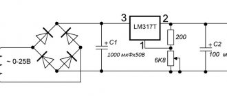
Scheme of a simple power supply based on IR2153.
The IR2153 is powered by 220 volts through a quenching resistor R1, a diode rectifier VD3, and a filter on C4. The generation frequency is set by elements C5, R2 (with the values indicated in the diagram, it turns out to be about 47 kHz). A transformer can be considered a program. The author's version used a power transformer from a computer power supply. The standard windings have been removed, the primary is wound into two cores with enamel insulated wire with a diameter of 0.6 mm.
The winding contains 38 turns. The layers are covered with electrical tape. The secondary is twisted into 7 cores with the same wire; to obtain 24V volts you need 7-8 turns; for other voltages, recalculate proportionally.
Design of a simple power supply.
The remaining elements of the diagram do not require separate explanations. The parts are placed on a printed circuit board, the transistors are mounted on a radiator.
PSU with overcurrent protection.
A more complex circuit with protection of transistors from overcurrent. The measurement is organized on transformer TV1. It is wound on a ferrite ring with a diameter of 12..16 mm. The secondary winding contains 50..60 turns in two wires with a diameter of 0.1..0.15 mm. Then the beginning of one winding is connected to the end of the second. The primary winding contains 1..2 turns. The protection response level is adjusted by potentiometer R13. When the set limit is exceeded, thyristor VD4 is triggered and the zener diode VD3 is bypassed. The supply voltage of the microcircuit is reduced to almost zero.
The power supply circuit provides a soft start. If generation has begun, the pulses from pin 6 through the divider R8R9 and capacitor C8 are rectified. Constant voltage charges C7 and opens transistor VT1. Capacitor C3 is connected to the frequency-setting circuit and the frequency of the microcircuit generator is reduced to the operating frequency.
Network filter circuits for pulsed and high-frequency interference: 4 types of designs
Rule No. 2: high-quality UPSs must have a reliable filter for high-frequency signals in the design of the unit .
It is important to understand that high frequency pulses play a dual role:
- V/h interference can come from the household network to the power supply;
- high-frequency current pulses are generated by the built-in converter and exit it into the home wiring.
Reasons for interference in a household network:
- aperiodic components of transient processes arising from switching powerful loads;
- operation of nearby devices with strong electromagnetic fields, for example, welding machines, powerful traction motors, power transformers;
- consequences of suppressed atmospheric discharge pulses and other factors, including the superposition of high-frequency harmonics.
Interference impairs the performance of electronic equipment, mobile devices and digital gadgets. They must be suppressed and blocked within the switching power supply design.
The filter is based on a choke made of two windings on one core.
Chokes can be made in different sizes, wound with thick or thin wire on large or small cores.
It is enough for a novice master to remember a simple rule: a filter with a large magnetic circuit inductor, an increased number of turns and a wire cross-section works better. (Principle: the more, the better.)
The inductor has inductive reactance, which sharply limits the high-frequency signal flowing through the phase or zero wire. At the same time, it does not have much effect on the current in the household network.
The operation of the inductor is effectively complemented by capacitive reactances.
The capacitors are selected in such a way that they short-circuit the interference signals weakened by the RF choke, directing them to ground potential.
The principle of operation of the filter for high-frequency noise from penetration of input signals into the power supply is shown in the picture below.
Y capacitors are installed between the ground potentials with zero and phase. Their design feature is that in the event of a breakdown they are not capable of creating an internal short circuit and supplying 220 volts to the device body.
Between the phase and zero circuits, capacitors are placed that can withstand 400 volts, or better yet, 630. They are usually shaped like a parallelepiped.
However, you should be well aware that the UPSs in the voltage converter themselves correct the signal and interference practically does not interfere with them. Therefore, such a system is relevant for conventional analog blocks with output signal stabilization.
For a switching power supply, it is important to prevent RF interference from entering the household network. Another solution implements this feature.
As you can see, the principle is the same. It’s just that capacitive reactances are always located along the path of the interference behind the inductor.
The third circuit of the high-frequency filter is considered universal. She combined elements of the first two. The Y capacitors in it simply work on both sides of each inductor.
The most expensive and reliable devices use a complex filter with additionally connected chokes and capacitors.
I immediately show the arrangement of filters on all circuits of the power supply: input and output.
Please note that a ferrite filter, consisting of two detachable half-cylinders or made of a one-piece structure, can be additionally installed on the cable coming out of the UPS and connected to the electronic device.
An example of its use is a switching power supply for a laptop. This is already the fourth use of the filter.
Is it possible to make a switching power supply with your own hands?
Sometimes purchasing a ready-made switching power supply is not economically feasible. In this case, if you understand electronics and know how to solder, you can make a switching power supply yourself. It is useful for powering various low-voltage power tools to avoid wasting the limited life of an expensive battery. You can also make a charger for a smartphone, laptop or other mobile gadgets.
Before you start making a power supply, you need to know where it will be used. Depending on the area of its application, the power of the product is determined. Power must be selected with reserve. It is believed that a switching power supply has the highest efficiency at a load of 60-90%.
In addition, you need to select a power supply circuit, and also determine whether the output should have a stable voltage and whether feedback needs to be introduced for this. Pay attention to its nominal parameters: voltage, current and power.
Adjustable width pulse generator circuit
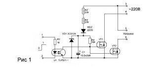
Bipolar symmetrical pulses of adjustable width can be obtained using a pulse generator according to the circuit in Fig. 1. The device can be used in circuits for auto-regulating the output power of switching power supplies. The DD1 chip (K561LE5/K561 LAT) contains a rectangular pulse generator with a duty cycle of 2.
The symmetry of the generated pulses is achieved by adjusting resistor R1. The operating frequency of the generator (44 kHz), if necessary, can be changed by selecting the capacitance of capacitor C1.
Rice. 1. Circuit of a shaper of bipolar symmetrical pulses of adjustable duration.
Voltage comparators are assembled on elements DA1.1, DA1.3 (K561KTZ); on DA1.2, DA1.4 - output keys. Rectangular pulses are supplied to the inputs of comparator switches DA1.1, DA1.3 in antiphase through forming RC diode chains (R3, C2, VD2 and R6, SZ, VD5).
The charging of capacitors C2, SZ occurs according to an exponential law through R3 and R5, respectively; discharge - almost instantly through diodes VD2 and VD5. When the voltage on capacitor C2 or SZ reaches the operating threshold of the comparator switches DA1.1 or DA1.3, respectively, they are turned on, and resistors R9 and R10, as well as the control inputs of the keys DA1.2 and DA1.4, are connected to the positive pole of the source nutrition. Since the switches are switched on in antiphase, such switching occurs strictly one by one, with a pause between pulses, which eliminates the possibility of through current flowing through switches DA1.2 and DA1.4 and the converter transistors controlled by them, if a bipolar pulse generator is used in a switching power supply circuit.
Smooth control of the pulse width is carried out by simultaneously applying a starting (initial) voltage to the inputs of the comparators (capacitors C2, SZ) from potentiometer R5 through diode-resistive chains VD3, R7 and VD4, R8. The maximum control voltage level (maximum output pulse width) is set by selecting resistor R4. The load resistance can be connected using a bridge circuit - between the connection point of elements DA1.2, DA1.4 and capacitors Ca, Cb. Pulses from the generator can also be supplied to a transistor power amplifier. When using a bipolar pulse generator in a switching power supply circuit, the resistive divider R4, R5 should include a regulatory element - a field-effect transistor, an optocoupler photodiode, etc., which allows, when the load current decreases/increases, to automatically adjust the width of the generated pulse, thereby controlling the output converter power. As an example of the practical implementation of switching power supplies, we provide descriptions and diagrams of some of them.
How to assemble: step by step instructions
For those who want to assemble a switching power supply with their own hands, here are several assembly diagrams.
Let's consider the circuit of a switching power supply with a power of up to 2 W. The rectifier and filter in it are assembled on resistor R1 (from 25 to 50 Ohms), diode VD1 and capacitor C1 (20.0 μF, 400 V). The high-frequency converter is a self-oscillator assembled on transistor VT1, transformer TR1, frequency-setting circuit resistor R2 (470 kOhm) and capacitor C2 (3300 pF, 1000 V). The voltage removed from the output winding of the transformer is rectified by diode VD2 and smoothed by electrolytic capacitor C3 (47 pF, 50 V).
Any transformer from a non-working transformer used in charging a mobile phone or other low-power power source will be suitable as a core for a transformer. Winding occurs in the following order:
- first we wind 200 turns of the primary winding with copper wire with a cross section of 0.08-0.1 mm;
- we isolate the primary winding and wind 5 turns of the base winding with the same wire;
- We wind the secondary winding. Wire diameter – 0.4 mm. The number of turns depends on what voltage you need to get at the output at the rate of one turn per volt.
We recommend reading: Kirchhoff's Law: first and second in simple words, formulas
Expert opinion Alexey Bartosh Specialist in repair and maintenance of electrical equipment and industrial electronics. Ask a question Attention! There should be a small non-magnetic gap between the halves of the magnetic core. Usually it is already present on cores taken from smartphone charger transformers. If there is none, place a layer of paper between the core halves.
We tighten the finished transformer with electrical tape or tape.
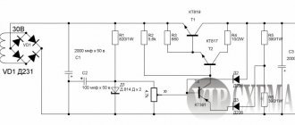
Let's consider a single-cycle power supply made using a self-excited self-oscillator circuit. Output voltage – 16 V, device power – 15 W.
At the input of the device, the alternating voltage of the electrical network is rectified using a diode bridge assembled on diodes D1-D4 (you can use any diodes rated for a voltage of 400 V and a current of 0.5 A, for example, N4007). Capacitor C1 (20 µF, 400 V) is responsible for smoothing out ripples. To prevent current surge when turned on, resistor R1 (25-50 Ohms) is used.
The initial bias based on transistor T1 (you can use 13003 or 13005) is set by resistor R2 (470 kOhm) and diode D6 (N4007). To smooth out voltage surges that occur when T1 is closed, the circuit includes elements such as: capacitor C2 (3300 pF 1000 V), diode D5 (N4007) and resistor R3 (30 kOhm 1 W, or you can use two 15 kOhm resistors).
The positive feedback pulses necessary to maintain the self-oscillation mode are supplied to the base T1 through resistor R4 (150 Ohm) and capacitor C3 (47 pF, 50 V). A chain consisting of T2, R5 (1.5 kOhm), D9 (zener diode KS515) is needed to stabilize the voltage.
The high-frequency converter is assembled using a flyback circuit. When T1 is open, energy is accumulated on the transformer, while diode D7 (KD213 is used in conjunction with a radiator with an area of 10 cm2) is in the closed state. After transistor T1 closes, the stored magnetic energy is released, diode D7 opens, current appears in the secondary circuit, capacitor C6 (100.0 μF, 25 V) is charged. Capacitors C4 (2200 pF) and C5 (0.1 µF) are needed to reduce interference. Stabilization of the output voltage occurs according to the scheme described below. When the device is connected to the network, the generator starts.
Voltage appears on the secondary winding. Capacitor C6 (100.0 µF, 25 V) is charging. When the voltage across it exceeds 16.3 V, the zener diode D9 (KS515) opens. Transistor T2 (KT603) opens and short-circuits the emitter junction T1. Transistor T1 closes, the generator stops working, and capacitor C6 begins to discharge. When the voltage at C6 becomes less than 16.3 volts, the zener diode D9 closes and closes T2. Thanks to this, T1 opens and generator operation resumes.
The primary winding w1 of the transformer is wound with 0.25 mm wire and has 179 turns. The base winding w2 contains two turns wound with the same wire. The secondary winding w2 consists of 14 turns of wire 0.6-0.7 mm.
You can take any low-power light bulbs, designed for a voltage from 24 to 36 V and a current from 100 to 200 mA.
Consider a switching power supply with an output power of 300 W.
The generator in this design is the TL494 integrated circuit. Control signals from the output of this IC are supplied alternately to MOS (MOSFET) transistors VT1 and VT2 (IRFZ34). Pulses from these transistors through a transformer and pulse shaper come to powerful transistors VT3 and VT4 (IRFP460). The converter is made using powerful transistors VT3 and VT4 in a half-bridge circuit.
All four windings of transformer TR1 are wound with 0.5 mm wire and contain 50 turns. In the TR2 transformer, the first winding consists of 110 turns of wire with a diameter of 0.8 mm. The number of turns of winding number two depends on the desired output voltage, at the rate of one turn per two volts. Winding three is wound with 12 turns of wire with a diameter of 0.8 mm.
⇡#Secondary circuit
The secondary circuit is everything that comes after the secondary winding of the transformer. In most modern power supplies, the transformer has two windings: 12 V is removed from one of them, and 5 V from the other. The current is first rectified using an assembly of two Schottky diodes - one or several per bus (on the highest loaded bus - 12 V - in powerful power supplies there are four assemblies). More efficient in terms of efficiency are synchronous rectifiers, which use field-effect transistors instead of diodes. But this is the prerogative of truly advanced and expensive power supplies that claim the 80 PLUS Platinum certificate.
The 3.3V rail is typically driven from the same winding as the 5V rail, only the voltage is stepped down using a saturable inductor (Mag Amp). A special winding on a transformer for a voltage of 3.3 V is an exotic option. Of the negative voltages in the current ATX standard, only -12 V remains, which is removed from the secondary winding under the 12 V bus through separate low-current diodes.
PWM control of the converter key changes the voltage on the primary winding of the transformer, and therefore on all secondary windings at once. At the same time, the computer's current consumption is by no means evenly distributed between the power supply buses. In modern hardware, the most loaded bus is 12-V.
To separately stabilize voltages on different buses, additional measures are required. The classic method involves using a group stabilization choke. Three main buses are passed through its windings, and as a result, if the current increases on one bus, the voltage drops on the others. Let's say the current on the 12 V bus has increased, and in order to prevent a voltage drop, the PWM controller has reduced the duty cycle of the key transistors. As a result, the voltage on the 5 V bus could go beyond the permissible limits, but was suppressed by the group stabilization choke.
The voltage on the 3.3 V bus is additionally regulated by another saturable inductor.
Stabilizing chokes and output filter (Antec VP700P)
A more advanced version provides separate stabilization of the 5 and 12 V buses due to saturable chokes, but now this design has given way to DC-DC converters in expensive high-quality power supplies. In the latter case, the transformer has a single secondary winding with a voltage of 12 V, and the voltages of 5 V and 3.3 V are obtained thanks to DC-DC converters. This method is most favorable for voltage stability.
DC-DC converter for 5 V bus (CoolerMaster G650M)
Output filter
The final stage on each bus is a filter that smoothes out voltage ripple caused by the key transistors. In addition, the pulsations of the input rectifier, whose frequency is equal to twice the frequency of the supply network, penetrate to one degree or another into the secondary circuit of the power supply.
The ripple filter includes a choke and large capacitors. High-quality power supplies are characterized by a capacitance of at least 2,000 uF, but manufacturers of cheap models have reserves for savings when they install capacitors, for example, of half the nominal value, which inevitably affects the ripple amplitude.
Design verification
Before turning on the power supply for the first time, you need to check it. First of all, the installation is checked; for example, traces of soldering or unwashed flux could remain. Any component installed on the board may be faulty.
If everything is in order with the installation, you can proceed to the second stage of testing using a light bulb. Any incandescent lamp can be used as a light bulb. To do this, we connect the power supply we made in series with the light bulb, as shown in the figure below.
If the light does not light, it means there is an open circuit in the power supply circuit. You need to check the board tracks, inductor, diode bridge.
The light is constantly on. There is a short circuit in the power supply. The reason may be a breakdown of capacitors or transistors. It is also necessary to check the tracks of the printed circuit board and the output circuits of the transformer.
If the light flashes and goes out, it means the power supply is working and the capacitors are charged.
Mains voltage rectifier: the most popular design
Rule No. 3: after the output from the filter, the voltage is supplied to the rectifier circuit , which in the basic version consists of a diode bridge and an electrolytic capacitor.
During the electrical conversion, the shape of a sine wave, consisting of half-waves of opposite signs, first changes to a signal in a positive direction after the diode assembly, and then these pulsations are smoothed out to an almost constant amplitude value of 311 volts.
Such a network voltage rectifier is included in the operation of all power supplies.