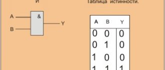
Trigger translated from English is a latch. This is an electronic module that can remain in one stable state for a long time and change it under the influence of an external signal. This is a digital automatic cell that can remember and store a binary data code of 1 bit in size. How a trigger works depends on its structure and purpose. At the heart of any such cell is a restoring ring consisting of a pair of inverters. The device contains direct and inverse outputs.
General block diagram of the latch
The place of flip-flops in digital circuitry
The PC trigger itself, as one of the structural elements in circuit design, does not contain any separate block or memory device. It is the simplest logical cell that remembers its previous and present states at the inputs and outputs. The memory is the result of the switch's operating algorithm. The device outputs are in a state of either logical zero or one. When they change, the circuit “latches” this position and remembers until the input control device, made of logical elements, gives a command to change the state.
Classification
Before considering the operation of triggers, it is necessary to understand the designations of the inputs and outputs of such devices.
Trigger - concept and classification
The inputs (ports) of a trigger are:
- R (reset) – sets position 0, separate port;
- S (set) – sets position 1, separate port;
- J – universal latches port, sets status to 1;
- K – port of universal latches, sets status 0;
- T – counting port, changes the position of the latch.
Information. A high potential level at the input or output is equal to a logical one, a low potential level is equal to a logical zero. For TTL brand microcircuits, a logical unit is considered to be a potential from 2.4...5V, a logical zero - 0...0.4 V at a supply voltage of 5 V. For logic assemblies of other series, the potential ranges may differ.
The latch has two output ports:
- Q – straight;
- Q¯ – inverse.
When one is on the direct line (Q = 0), the “latch” is in the “1” state. In case of low potential at the output (Q = 1), the latch status is “0”.
The opposite is true for the inverse output. When output Q¯ is zero, the switch is in the one state. Position inversion is needed to implement various schematic solutions.
Attention! The types of ports determine the names of electronic switches, so, having ports R and S, it is called RS flip-flop.
A sequential logic device (PLD), which is a “latch,” is a kind of block for constructing various combinations in logical circuit circuits. The bistable state of the RS latch helps layout logic circuits such as counters, holding registers, memory devices, or shift registers. Regardless of the method of arranging logical connections, the main types of electronic switches can be divided according to the method of data input:
- synchronous type;
- asynchronous type;
- combined.
It all depends on how the control command is sent to change the state of the “latch”.
Synchronous devices
To ensure that the rs trigger does not change its position due to the combination of delayed command pulses on its ports, a synchronizing command is used. This is a clock pulse that is sent to the clock port. The changed signals at the inputs of such a “latch” will not be able to change the state at the output until a clock (synchronizing) pulse arrives. These pulses are generated by clock generators. The length of clock signals is much less than their period. Pulses determine the frequency of information replacement, linking it to discrete time periods - tl, t2,...,tn-1,tn, tn+l. This allows you to synchronize the operating processes of individual equipment units in a single rhythm.
The action of the scheme is as follows:
- if there is a zero on port C, the status of the flip-flop does not change, since information from ports S and R is not transmitted to the latch;
- if a logical one appears on port C, then the switch accepts commands from the S and R inputs and changes its position.
Such circuits have increased noise immunity, which distinguishes them favorably from asynchronous devices; the latter can turn over not only from the signal, but also from interference. The synchronous structure is used in technology related to the conversion or processing of digital data.
Synchronous RS - Trigger, Circuit and Graphic Symbol
Important! When using an RS latch with inverse inputs, it is necessary to replace the elements of the “AND” circuit with “AND - NOT” elements.
Asynchronous Models
A device that changes its state immediately when the command on the logical ports changes is called an asynchronous trigger. It contains only ports: R (reset) and S (installation). The limitations for using such circuits are associated with competition between signals, which, when they hit different inputs of the RS flip-flop, move in different ways, as if competing with each other. In this case, temporary delays and shifts occur due to various reasons: temperature changes, long service life, etc. This “race” causes frequent erroneous cell flips.
Clock synchronization in this case is not effective, therefore asynchronous cells are used as asynchronous counters, various switches, frequency dividers and similar circuit solutions.
Asynchronous RS flip-flop, block diagram
Combined schemes
A module consisting of a combination of several cells is called a combined trigger. Combinations of two or more functional cells are possible.
Table of combinations of two types of memory cells
| Device type | R.S. | R | S | E | JK | T | D | D.V. |
| R.S. | X | X | X | X | X | X | X | |
| R | X | X | X | X | X | X | ||
| S | X | X | X | X | X | |||
| E | X | X | X | X | ||||
| JK | X | X | X | |||||
| T | X | X | ||||||
| D | X | |||||||
| D.V. |
Types of triggersHere X - combining two types is possible.
The division of these devices by type can be considered using state transition tables.
The following types of state memory cells are distinguished:
- rs-latch – asynchronous and synchronous;
- jk-latch;
- d-latch;
- t-latch.
The last element of the list is a composite device, executed from a synchronous rs-memory cell.
RS triggers
Two types of such cells are considered: asynchronous and synchronous latch. Upon closer examination, a significant difference in operation and scope of application is visible.
RS trigger asynchronous
The simplest type of latch, rarely used as an independent device, is a cell for constructing more complex blocks. Asynchronous cells were built on the elements:
- 2 OR – NOT, trigger cell with direct ports;
- 2 NAND, trigger cell with inverse ports.
Fixed trigger positions provide feedback. This is connecting the output of one to any input port of another logic element.
RS trigger synchronous
The basis of registers, frequency dividers and various counters is the trigger memory cell. In such devices, previously recorded information must be transferred to the output and written to the next cell using a clock pulse signal. The pulse is sent to the C-port (static or dynamic).
For your information. The static C-input synchronizes by changing the signal potential level, the dynamic C-input synchronizes the change in state not by the level, but by the moment of its change. Switching at the dynamic C-input can be carried out along the edge of the pulse (direct) or along its cut (inverse).
Consisting of a pair of synchronous RS flip-flops and an inverter, two-stage RS flip-flops are driven by a full (both edge and edge) dynamic clock pulse. Such memory cells are called master-slave (master-assistant).
JK trigger
A distinctive feature of this type of “latch” is the absence of a prohibited combination of signals on the ports. When J = K = 1, the latch position is reversed compared to the current Q0.
The JK switch differs from the RS memory cell in only one way: if “1” is applied to J and K, then it changes its position to the opposite position. An inversion occurs, and this memory cell does not have the prohibited states of the main ports.
Attention! If we draw an analogy with the designation of inputs, then J and K, respectively, are similar to the S and R inputs of an RS flip-flop. Only synchronous jk flip-flops with dynamic synchronization have found practical application.
Truth table and jk flip-flop notation
What is RS trigger
This is a memory cell capable of being in one of the stable positions: “0” or “1”. Turn over, i.e. it can change them under the influence of clock signal pulses. An elementary element assembled on two inverters cannot write or erase a stored bit. The operating principle of rs flip-flops, made on two 2I-NOT components, allows this to be done.
Basics of electroacoustics
A trigger is a logical circuit with positive feedback that has two stable states - one and zero, which are designated 1 and 0, respectively (Fig. 23.1, a). At the heart of any trigger is a ring of two inverters (Fig. 23.1, b, c). A trigger is a memory element of sequential logic devices; in diagrams it is designated by the letter T
When power is applied as a result of transient processes, one of the inverters is arbitrarily set to the unit state, and the other to the zero state. Subsequently, the state of the logic elements (LE) is preserved, since the signal from the output of one LE maintains the state of the other LE. It is generally accepted to call such a circuit a memory element or latch.
Trigger inputs are divided into information and control (auxiliary). This division is largely arbitrary.
Information inputs are used to control the trigger state. Control inputs are typically used to preset a flip-flop to some state and for synchronization. As a rule, triggers have 2 outputs: direct and inverse.
Rice. 23.1. Trigger block diagram
Triggers are classified according to the method of receiving information, the principle of construction and functionality.
Based on the method of receiving information, a distinction is made between asynchronous and synchronous triggers. An asynchronous trigger changes its state immediately at the moment the corresponding information signal appears.
Synchronous triggers respond to information signals only if there is a corresponding signal at the so-called synchronization input C (from the English clock). This input is also designated by the terms “strobe”, “tact”.
Synchronous flip-flops, in turn, are divided into flip-flops with static (static) and dynamic (dynamic) control via the synchronization input C.
Static triggers perceive information signals when a logical one (direct input) or logical zero (inverse input) is applied to input C.
Dynamic triggers perceive information signals when the signal at input C changes (changes) from 0 to 1 (direct dynamic C-input) or from 1 to 0 (inverse dynamic C-input).
According to the method of construction, one- and two-stage triggers are distinguished. A single-stage trigger has one stage of storing information, and a two-stage trigger has two such stages. First, information is recorded in the first stage, and then rewritten into the second and appears at the output. A two-stage trigger is designated TT.
Based on functionality, triggers are divided into the following classes:
- — with separate setting of state 0 and 1 (RS triggers);
- — universal (JK-triggers);
- - with receiving information via one input D (D-flip-flops, or delay triggers);
- — with a counting input T (T-flip-flops).
Flip-flop inputs are usually designated as follows:
- — S – input for setting to state “1”;
- — R – input for setting to state “0”;
- — J – input for setting to state “1” in a universal trigger;
- — K – input for setting to state “0” in a universal trigger;
- — T – counting (common) input;
- — D – input for setting to state “1” or state “0”;
- — V – additional control input to allow receiving information (sometimes the letter E is used instead of V).
Let's look at some types of triggers and their implementation on logical elements.
The symbolic graphical symbol of an asynchronous RS trigger and a table of its transitions are shown in Fig. 23.2.
Rice. 23.2. RS trigger
The trigger has two information inputs: S (from the English set) and R (from the English reset). It is convenient to describe the law of operation of triggers using a transition table, which is sometimes also called a truth table (Fig. 23.2). St, Rt, Qt denote the corresponding logical signals occurring at some time t, and Qt+1 the output signal at the next time t+1.
The combination of input signals St = 1, Rt = 1 is often called forbidden, since after it the trigger finds itself in a state (1 or 0), which is impossible to predict in advance. Such situations should be avoided.
The trigger in question can be implemented on two elements OR-NOT (Fig. 23.3,a) or AND-NOT (Fig. 23.3,b).
These circuits operate in full accordance with the above transition table, which is shown in Fig. 23.2 is given in abbreviated form. The complete truth table (transition table) of an RS flip-flop using NOR elements is as follows (Fig. 23.4).
Rice. 23.3. RS trigger on NOR (a) and NAND (b) elements
Rice. 23.4. Truth table of an RS flip-flop based on NOR elements
In an asynchronous RS flip-flop on NAND elements, switching is performed by a logical “0” applied to the R or S input, i.e., the inverse of the previously discussed transition table is implemented (Fig. 23.4). A prohibited combination corresponds to logical “0” at both inputs.
The K564TP2 microcircuit contains 4 asynchronous RS triggers and one control input (Fig. 23.5). When a low level is applied to the V input, the trigger outputs are disconnected from the microcircuit pins and go into the third (high-impedance) state. When a logical signal “1” is applied to input V, the flip-flops operate in accordance with the above transition table.
Rice. 23.5. RS trigger K564TP2
Consider a synchronous RS flip-flop (Fig. 23.6). If input C is logical “0”, then both the output of the upper input element “AND-NOT” and the output of the lower one will be logical “1”. And this, as noted above, ensures the storage of information. Thus, if the input C is logical “0”, then the influence on the inputs R, S does not lead to a change in the state of the trigger. If a logical one is applied to the synchronization input C, then the circuit reacts to input signals in the same way as the one discussed earlier.
In the RS flip-flops with feedback discussed above, uncertainties are possible due to the simultaneous change of information at the direct and inverse outputs associated with the R and S inputs. To eliminate this effect, two-stage triggers are used.
When using a two-stage RS trigger (Fig. 23.7), it is possible to connect its inputs and outputs. A two-stage flip-flop consists of two synchronous RS flip-flops and an additional NOT element. When input control signals and a clock signal are supplied (Fig. 23.8), information is written to the first trigger (moment t1). In this case, the second trigger does not change its state, since a logical zero is supplied to its synchronizing input from the inverter. Only after finishing writing to the first trigger when the clock signal changes from one to zero is writing to the second trigger of the two-stage system (t2).
Rice. 23.6. Synchronous RS trigger
Rice. 23.7. Block diagram of a two-stage trigger
Rice. 23.8. Timing diagram of a two-stage trigger
Thus, the two-stage flip-flop switches on the falling edge of the clock pulse. This synchronization is called dynamic. The presence of dynamic synchronization is indicated by a slash. The use of two stages in a trigger is indicated by two letters CT.
Let's consider as an example an RS flip-flop of type 136TP1 - a synchronous flip-flop. The trigger has complex inputs R and S, which cause a change in the state of the trigger when the front of the clock pulse acts (a difference from 0 to 1). Information inputs R and S have input logic “3I” (Fig. 23.9).
Inputs R and S (pins 2 and 13) – setting inputs (settings 1 and 0, respectively) operate independently whether a clock pulse is applied or not.
Rice. 23.9. Synchronous RS trigger K136TP1: a – UGO, b – truth table
The table (Fig. 23.10, b) uses the following notation:
- - any state of S, R-signals at pins 2, 13 of the IC;
- – product of signals at pins 9, 10, 11 of the IC;
- – product of signals at pins 3, 4, 5 of the IC.
Truth table
D trigger - edge-controlled device and elements
The state transition table (truth table) explains the operation of an RS flip-flop using NAND elements. On it, Q 0 is the current status of the cell before the active signal hits the port. When there is no logical one at the inputs R and S, the “latch” maintains position Q 0. An active pulse R = 1 moves the latch to position 0, a pulse S = 1 to position 1. The asterisk in the table indicates the position when the combination of incoming signals is prohibited.
RS flip-flop truth table
This type has separate assignment of logical states of zero and one across information ports.
Brief theoretical information
Triggers are designed to store binary information. The use of triggers makes it possible to implement RAM devices (that is, memory in which information is stored only for the duration of calculations).
However, flip-flops can also be used to build some digital memory devices, such as counters, serial-to-parallel converters, or digital delay lines.
RS trigger
The main trigger on which all other triggers are based is the RS trigger. The RS trigger has two logical inputs:
- R – setting 0 (from the word reset);
- S – setting 1 (from the word set).
The RS trigger has two outputs:
- Q – straight;
- Q - reverse (inverse).
The state of the trigger is determined by the state of the direct output. The simplest RS flip-flop consists of two logic elements covered by cross positive feedback.
Let's look at how the trigger works:
Let R=0, S=1. The lower logical element performs the logical OR-NOT function, i.e. 1 at any of its inputs leads to the fact that its output will have a logical zero Q=0. The output Q will be 1 (Q=1), because zeros are supplied to both inputs of the upper element (one zero from input R, the other from output). The trigger is in a single state. If we now remove the setting signal (R=0, S=0), the situation at the output will not change, because Although the lower input of the lower logic gate will receive a 0, its upper input will receive a 1 from the output of the upper logic gate.
It will be interesting➡ What is a bridge rectifier and how does it work?
The flip-flop will remain in the single state until a reset signal is received at the R input. Let now R=1, S=0. Then Q=0, a =1. The trigger switched to “0”. If after this you remove the reset signal (R=0, S=0), then the trigger will still not change its state. To describe the operation of a trigger, a table of states (transitions) is used. Let's denote:
- Q(t) – state of the trigger before the arrival of control signals (changes at inputs R and S);
- Q(t+1) – trigger state after changes at inputs R and S.
Transition table of RS flip-flop in NOR basis
| R | S | Q(t) | Q(t+1) | Explanations |
| Information storage mode R=S=0 | ||||
| 1 | 1 | |||
| 1 | 1 | Unit setting mode S=1 | ||
| 1 | 1 | 1 | ||
| 1 | Zero setting mode R=1 | |||
| 1 | 1 | |||
| 1 | 1 | * | R=S=1 prohibited combination | |
| 1 | 1 | 1 | * |
An RS trigger can also be built using “AND-NOT” elements (Figure 2.2).
Inputs R and S are inverse (active level “0”). The transition (switching) of this trigger from one state to another occurs when one of the inputs is set to “0”. The combination R=S=0 is prohibited.
Transition table of RS flip-flop in the “2AND-NOT” basis
| R | S | Q(t) | Q(t+1) | Explanations |
| * | R=S=0 prohibited combination | |||
| 1 | * | |||
| 1 | Zero setting mode R=0 | |||
| 1 | 1 | |||
| 1 | 1 | Unit setting mode S=0 | ||
| 1 | 1 | 1 | ||
| 1 | 1 | Information storage mode R=S=1 | ||
| 1 | 1 | 1 | 1 |
Synchronous RS trigger
The RS flip-flop circuit allows you to remember the state of the logic circuit, but since a transient process may occur when the input signals change (in digital circuits this process is called “dangerous races”), you need to remember the states of the logic circuit only at certain moments in time, when all transient processes are completed, and the signal at the output of the combinational circuit corresponds to the function it performs. This means that most digital circuits require a synchronization signal (clock signal).
All transient processes in a combinational logic circuit must end during the period of the clock signal supplied to the inputs of the flip-flops. Flip-flops that remember input signals only at the time specified by the synchronization signal are called synchronous. A schematic diagram of a synchronous RS flip-flop is shown.
Transition table of synchronous RS flip-flop
| R | S | C | Q(t) | Q(t+1) | Explanations |
| 1 | Information storage mode R = S = 0 | ||||
| 1 | 1 | 1 | |||
| 1 | 1 | 1 | Unit setting mode S =1 | ||
| 1 | 1 | 1 | 1 | ||
| 1 | 1 | Zero setting mode R=1 | |||
| 1 | 1 | 1 | |||
| 1 | 1 | 1 | * | R = S = 1 prohibited combination | |
| 1 | 1 | 1 | 1 | * |
In table 2.3. By signal C we mean a sync pulse. Without a clock pulse, a synchronous RS flip-flop retains its state.
Timing diagrams
Switching voltage stabilizer
In addition to truth tables, a timing diagram helps to understand the operation of a bit memory cell. In this case, the following parameters are considered on the graph when studying pulses:
- pulse duration – time interval from rise to fall;
- period – the interval from the front of the previous pulse to the front of the next one;
- duty cycle – the ratio of the pulse period to its duration.
The diagram graphically displays the signal pulses at the inputs and outputs at the same time points.
RS flip-flop timing diagram
Classification of sequential circuits
Sequential circuits can be classified according to the following indicators:
- single-stage latches, which contain a memory element and a control device, are marked with the letter T;
- two-stage cells: static and dynamic control, used to protect against signal races, designated by the letters TT;
- switches with complex logic: single- and two-stage cells.
Single-stage cells are used as the first stages in CT switches with a dynamic control circuit and have the same control. When used independently, the controls are mostly static.
Two-stage devices have both static and dynamic control.
Status "Installed"
The RS switch in this state has an established circuit with Q equal to zero and Q¯ equal to one, and is independent of the controlled signal. In this case, there is a zero on R, and a logical one on S.
Status "Reset"
This is also an unchanged situation. To organize it, it is necessary to set the initial conditions. “1” is supplied to R, “0” to S. In this case, the output Q should have a value of “1”, Q¯ – the value of “0”. Feedbacks provide and fix a value independent of subsequent input values.
Trigger classification
- by the method of receiving information;
- according to the principle of construction;
- by functionality.
Asynchronous trigger
Asynchronous trigger - changes its state immediately at the moment the corresponding information signal appears.
Vasiliev Dmitry Petrovich
Professor of Electrical Engineering, St. Petersburg State Polytechnic University
Synchronous triggers - react to information signals only if there is a corresponding signal at the so-called synchronization input C (from the English clock). This input is also designated by the terms “strobe”, “tact”.
Synchronous triggers
Synchronous flip-flops, in turn, are divided into flip-flops with static (static) and dynamic (dynamic) control via the synchronization input C. Static flip-flops perceive information signals when a logical one (direct input) or a logical zero (inverse input) is applied to input C.
Dynamic triggers perceive information signals when the signal at input C changes (changes) from 0 to 1 (direct dynamic C-input) or from 1 to 0 (inverse dynamic C-input).
Static triggers
Static triggers, in turn, are divided into single-stage (single-cycle) and two-stage (push-pull). A single-stage trigger has one stage of storing information, and a two-stage trigger has two such stages. First, information is recorded in the first stage, and then rewritten into the second and appears at the output. A two-stage trigger is designated by TT.
RS trigger switching diagram
The switching, setting and reset states can be viewed in the timing diagram. It is noted that the switch goes into the setting position when a zero appears at its S-input and a one at the R input, a fixed reset when a zero appears at the R port and a one at S.
Latch Switching Diagram
Attention! If zero is applied to two inputs (R and S) synchronously, then the switch, due to an uncertain state at the inputs, can flip to any unpredictable position, resulting in data corruption.
RS flip-flop on logic elements
The simplest way to do this is to connect a pair of two-input NAND gates together. In this case, feedback from the output of one element is fed to the input of another (see diagram below).
As a rule, in this circuit, input signals are shown inverted (with an upper underscore), although in the future, when analyzing the operation, the designations of direct (non-inverted) inputs are used. This makes it very difficult to understand the logic of the trigger. Therefore, we will not introduce input inversion at the stage of considering the operation of the circuit using NAND elements, but will take this into account later when modifying it.
How many inputs and outputs does an RS flip-flop have? From the diagram above it can be seen that it contains an S-input and an R-input, which serve, respectively, to set and reset the circuit, as well as direct Q and inverse Q̃ outputs. But this simplest trigger is of the asynchronous type, its symbol is shown below.
The synchronous device also has a C input for clock pulses.
Trigger circuit modification
the rs rises , it is necessary to have at its outputs:
- during installation – Q = 1, and Q¯ = 0;
- at reset – Q = 0, and Q¯ = 1.
To organize this, the incoming latch signals are inverted. As a result, a state change is performed when positive signals are received. When modified, 2 NAND elements are added as inverters.
Trigger circuit modification
D – trigger
The D-flip-flop has 1 information input (D-input). There are only synchronous D-flip-flops. The state of the information input is transmitted to the output under the action of a clock pulse (input C).
D flip-flop transition table
| C | D | Q(t) | Q(t+1) | Explanations |
| * | Information storage mode | |||
| * | 1 | 1 | ||
| 1 | * | Information recording mode | ||
| 1 | 1 | * | 1 |
If input D is “1”, then upon arrival of the clock pulse Q = 1. If input D is “0”, then Q = 0.
How to synchronize trigger operation
Connecting a two-port “AND” element into a serial circuit of the trigger circuit with each of the inputs will allow you to change its status, regardless of the states at the R, - or S-inputs. A new port C is obtained by combining the two ports of the “I” cells. As a result of the modification, the status at the outputs Q and Q¯ will change only when a high potential arrives at C. It is possible to connect clock generators to this new input.
Trigger Synchronization
Universal trigger (JK trigger)
Such a trigger has information inputs J and K, which in their influence are similar to the inputs S and R of a clocked RS trigger:
- when J=1, K=0, the clock pulse trigger is set to state Q=1;
- when J= 0, K=1 – switches to state Q=0;
- when J=K=0 – stores previously received information.
But unlike a synchronous RS flip-flop, the simultaneous presence of logical 1s at the information inputs is not a prohibited combination for a JK flip-flop and leads the flip-flop to the opposite state.
JK flip-flop transition table
| K | J | C | Q(t) | Q(t+1) |
| 1 | ||||
| 1 | 1 | 1 | ||
| 1 | 1 | 1 | ||
| 1 | 1 | 1 | 1 | |
| 1 | 1 | |||
| 1 | 1 | 1 | ||
| 1 | 1 | 1 | 1 | |
| 1 | 1 | 1 | 1 |
Digital electronics – YB-triggers with dominant Y-input
The presence of forbidden combinations for clocked &Y flip-flops gave rise to the idea of building a trigger that forcibly sets Qx to 0 at S = 1 and R = 1 when a clock pulse is applied. This becomes possible thanks to a special connection of the inputs. In Fig. Figure 7.35 shows such a connection of inputs. When S = 1 and R = 1, the 1-signal cannot affect the flip-flop, since the output of the element is NOT 0. The AND-element is locked. 1-signal on R allows reset. The setting mode with S = 1 and R = 0 remains possible, since now the output of the NOT element is 1 and the AND element has a 1 at the output.
Interesting article: What is a solid state relay?
Such a trigger is called an .RS'-trigger with a dominant /?-input, or a ^trigger. The rule of its operation follows from the symbol in Fig. 7.36 (see also section 7.1). It says: if both inputs of the trigger S, R and input T have level 1, then with a synchronization signal 1 Q{ is set to 0, and Q2 is set to 1. The truth table of a clocked LU flip-flop with a dominant R-input is shown in Fig. 7.37. Of course, there is also a clocked RS flip-flop with a dominant ^-input (see reference test).
It will be interesting➡Safety rules when working with electricity
Registers on flip-flops
Since a single switch is a single-bit memory cell, to store multiple bits, the number of unit stores must be increased. A chain of such cells is called a register. The register allows you to temporarily store digital data of binary bits. The number of bits depends on the number of one-bit cells.
Circuit of a 4-bit shift register on flip-flops
The use of elementary electronic digital devices - flip-flops, allows you to create complex control circuits for logical devices. One elementary memory latch, with its bistable state, helps implement the most complex circuit designs.