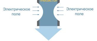
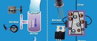
Briefly about MOSFET
A MOSFET is a controlled switch with three contacts (gate, drain and source). The gate (control) signal is supplied between gate and source, and the switching contacts are drain and source. The gate itself is made of metal and is separated from the source by a metal oxide as a dielectric. This reduces power consumption and makes this transistor an excellent choice for use as an electronic switch or amplifier in a common-source circuit.
To operate properly, MOSFETs must maintain a positive temperature coefficient. Losses in the on state are small and theoretically the resistance of the transistor in this state is not limited - it can be close to zero. Additionally, since MOSFETs can operate at high frequencies, they can operate in fast switching applications with low switching losses.
There are many different types of MOSFETs, but the most comparable to IGBTs are power MOSFETs. They are specifically designed to handle significant power levels and are most often used only in the on or off states, making them the most used switch for low voltage circuits. Compared to IGBTs, power MOSFETs offer the advantages of faster switching speed and higher efficiency when operating at low voltages. Moreover, such a circuit can withstand high blocking voltage and support high current. This is due to the fact that most high-power MOS structures are vertical (rather than flat). The nominal voltage is a direct function of the doping and thickness of the N-doped epitaxial layer, and the current depends on the channel width (the wider the channel, the higher the current).
Description
A field-effect transistor, also known as a mosfet (MOSFET), is an electronic component that allows, using a small voltage and current (from a microcontroller pin), to control a powerful DC load that the MK pin itself is not able to power: motors, valves, powerful LEDs, and so on. . More details about mosfets are written in the lesson on load control. The lesson includes an IRF740 mosfet, N-channel type.
Basic parameters of a MOSFET transistor
Listed below are the main parameters of the MOSFET transistor, the data for which is given in the data sheets:
1. Maximum drain-source voltage (Drain-Source Voltage) VDS - the maximum permissible voltage between the drain and source of the transistor.
2. Drain-source resistance RDS - resistance between drain and source in the open state. At a given gate-source voltage. And the drain current.
3. Maximum gate-source voltage (Gate-Source Voltage) VGS – maximum gate-source control voltage. If this voltage is exceeded, breakdown of the gate dielectric and failure of the transistor is possible.
4. Maximum drain current in continuous mode (Continuous Drain Current) ID – maximum value of constantly flowing drain current in continuous mode. Depends on the temperature of the transistor body and heat dissipation conditions.
5. Maximum pulsed drain current (Pulsed Drain Current) IDM - maximum value of pulsed drain current. Depends on the fill factor and heat removal conditions. Fundamentally limited by the dissipation energy of the crystal.
6. Crystal dissipation energy (Single Pulse Avalanche Energy) EAS is the maximum energy that can be dissipated on a transistor crystal without destroying it.
7. Maximum Power Dissipation PD – the maximum thermal power that can be removed from the transistor body (at a given temperature of the transistor body).
8. Operating temperature range - the temperature range within which the transistor can be operated.
8. Thermal resistance of the transistor-to-air RthJA (Maximum Junction-to-Ambient) - the maximum thermal resistance of the transistor to air (subject to free convective heat exchange).
9. Thermal resistance of the transistor body - heat sink (Case-to-Sink, Flat, Greased Surface) RthCS - maximum thermal resistance of the junction of the transistor body - heat sink. Provided the heat sink has a flat, shiny surface.
10. Thermal resistance of the transistor body (Maximum Junction-to-Case (Drain) RthJC - maximum thermal resistance of the crystal - transistor body.
We recommend reading: The simplest low-frequency amplifiers using transistors
11. Gate-Source Threshold Voltage VGS(th) - gate-source threshold voltage at which the transistor begins to transition to the conducting state.
12. Zero Gate Voltage Drain Current IDSS – drain current of the turned off transistor (at zero gate-source voltage). Significantly depends on temperature.
13. Gate leakage current (Gate-Source Leakage) IGSS - current through the gate at a certain (usually maximum) gate-source voltage.
14. Input Capacitance Ciss – the total gate-source capacitance and gate-drain capacitance (at a certain drain-source voltage).
15. Output Capacitance Coss – the total gate-drain capacitance and drain-source capacitance.
16. Reverse Transfer Capacitance Crss – gate-drain capacitance.
17. Total gate charge (Total Gate Charge) Qg – the total gate charge required to transfer the transistor to a conducting state.
18. Gate-Source Charge Qgs – charge of the gate-source capacitance.
20. Gate-Drain Charge Qgd - charge of the gate-drain capacitance.
21. Turn-On Delay Time td(on) – the time during which the transistor accumulates charge to the gate voltage at which the transistor begins to open.
22. Rise Time of the current through the transistor – the time during which the transistor drain current increases from 10% to 90%.
23. Turn-Off Delay Time td(off) – the time during which the gate charge becomes less than the turn-on charge, and the transistor begins to close.
24. Fall Time of the current through the transistor (Fall Time) - the time during which the transistor drain current decreases from 10% to 90%.
25. Internal Drain Inductance LD – parasitic inductance of the drain terminal of the transistor.
26. Internal Source Inductance LS – parasitic inductance of the transistor source terminal.
27. Constant forward current through the reverse diode (Continuous Source-Drain Diode Current) IS - the maximum value of the constantly flowing forward current through the parasitic pn diode.
28. Pulsed Diode Forward Current ISM - the maximum value of the constantly flowing forward current through the parasitic pn diode.
29. Body Diode Voltage VSD – forward voltage drop across the diode. At a given temperature and source current.
30. Body Diode Reverse Recovery Time trr - recovery time of the reverse conductivity of the parasitic diode.
31. Body Diode Reverse Recovery Charge Qrr – the charge necessary to restore the reverse conductivity of the parasitic diode.
32. Forward Turn-On Time ton - time of transition of the diode to the conducting state. Usually it is negligibly small.
33. Gate resistance RG – parasitic series gate resistance. It is this that limits the switching speed with a control driver with a large output current.
Dynamic characteristics
The dynamic properties (switching speed, losses) of MOSFET modules depend on the features of their structure, the magnitude of parasitic junction capacitances and terminal resistance. Unlike the “ideal” switch, controlled by an insulated gate without power loss, controlling a real MOSFET consumes the energy necessary to recharge the input capacitors. Obviously, the control power depends on the size of these capacitors and the switching frequency.
In addition, the switching process is influenced by parasitic inductances of the power connections inside the transistor and external switching circuits. Their presence leads to the formation of voltage surges when turned off, as well as oscillations in parasitic circuits.
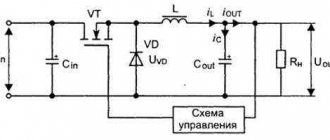
The behavior of MOSFET switches in pulsed operating mode can be analyzed using an equivalent circuit:
- When the transistor is turned off, the capacitance CGD is small and approximately equal to CDS.
- When the transistor is turned on, the capacitance CGD increases rapidly from the moment the control signal VGS exceeds the drain-source voltage, the reason for this is the inversion of the layer under the gate region.
- The technical characteristics, as a rule, indicate the values of the capacitances Ciss, Cres, Coss of the switched-off transistor (Table 2).
Table 2. Small Signal MOSFET Capacitances
| Input capacitance | Ciss = CGS+CGD |
| Reverse capacitance (Miller) | Cres = CGD |
| Output Capacitance | Coss = CGD+CDS |
Small-signal MOSFET capacitance values are not of much practical significance since they are very dependent on the operating voltage (this was described in detail earlier). The behavior of the MOSFET in the “hard” switching mode of an active-inductive load with a continuous current (when the load time constant L/R is much greater than the operating frequency period) is described below. The main diagrams of currents and voltages, by analogy with the processes discussed earlier for IGBT, are shown in Fig. 13.
In addition to the “non-ideal” parameters of transistors and diodes, switching losses and the position of the operating point are significantly influenced by passive distributed elements of the switching circuit.
Inclusion
As shown in Fig. 13, the drain-to-source voltage of the power MOSFET drops to saturation level in about 10 ns, its value is determined by the formula VDC(on) = ID × RDS(on).
During the time interval 0–t1, the transistor remains blocked. Gate current IG begins to flow when the control signal appears, it charges the capacitance CGS until the charge on it reaches the level QG1. The voltage VGS increases linearly with a time constant determined by the CGS and the gate resistor RG. Since the control signal level is still below the VGS(th) threshold, the MOSFET channel remains closed.
In the time interval t1–t2, the drain current ID begins to increase when the gate voltage reaches the level VGS(th) (time t1). The ID value is related to the control signal through the transconductance gfs (ID = gfs × VGS), and the gate voltage is increased to the value VGS1 = ID/gfs (t2). Since the opposed diode can block the flow of current only at time t2, the voltage VDS before this decreases insignificantly. At t = t2, the gate charge reaches the value QG2.
During this time interval, the largest part of the turn-on losses Eon is generated in the transistor. As long as ID < IL and some of the current IL still continues to flow through the box diode, the level of VDS cannot become much lower than the supply voltage VDD. The difference between VDD and VDS, marked in Fig. 13, is mainly caused by transient dynamic signal drop on the parasitic inductances of the switching circuit.
The time interval t2–t3 corresponds to a fully turned on transistor. When the box diode is turned off, the drain-source voltage drops to the saturation level VDS(on) = ID×RDS(on). Between times t2 and t3, the drain current and gate voltage are still coupled through the transconductance parameter, and VGS remains virtually unchanged. After the MOSFET turns on, the gate current IG discharges the Miller capacitance to the level (QG3–QG2). At t = t3, an amount of charge equal to QG3 remains on the gate. When all the load current IL begins to flow through the open channel of the MOSFET, the box diode begins to turn off. The reverse recovery process of the diode causes the drain current ID to exceed IL by an amount IRR (reverse recovery current) during time trr, and the transistor dissipates additional energy due to the charge Qrr.
The time interval t3–t4 corresponds to the ohmic region of the characteristic. At moment t3, the transistor is turned on, its operating point has passed the active zone and reached the boundary of the ohmic working region. The control signal VGS is no longer coupled to the current ID through the transconductance gfs. The accumulation of gate charge (QGtot–QG3) leads to a further increase in VGS, reaching the level of the output voltage of the driver VGG.
Shutdown
When the field effect transistor is turned off, all processes occur as described above, but in reverse order. The charge QGtot must be absorbed by the reverse gate current, and, unlike IGBTs, power MOSFETs do not need to be turned off with a negative voltage (VGSoff = 0). During the shutdown process, it is necessary to discharge only the MOSFET's own capacitances to a level where the influence of charge carriers on the channel region ceases.
The drain overvoltage noted in Fig. 13 at the moment of switching off, is caused by the presence of parasitic inductances in the switching circuit, its level is proportional to the rate of current decay dID/dt.
Rice. 13 . Diagrams of currents and voltages in the “hard” switching mode of MOSFET and IGBT with an opposed diode to an active-inductive load
The more a MOSFET's switching behavior deviates from "ideal hard switching", the more distorted the gate step response becomes.
Connection (N-channel)
The mosfet control pin (gate) is connected to any digital pin of the MK through a 100-200 Ohm current-limiting resistor, which will protect the pin from too much current. It is also pulled up to GND with a 10 kOhm resistor so that the transistor automatically closes in the absence of a signal from the MK. The “plus” of the power supply is connected directly to the load, GND is connected to GND of the microcontroller. GND of the load is connected to the output (drain) of the mosfet:
Let's consider the possible connection of a motor from the PRO version of the kit, powered by an external 5V adapter:
When switching an inductive load (motors, electromagnets, solenoids and other “coils”), a voltage surge occurs that can damage the transistor. To protect against it, we placed a diode (included in the kit) parallel to the motor; the diode will take the entire blow.
Drivers for management
Since there is no current in the control circuit, standard circuits do not need to be used in static mode. It makes more sense to use a special driver - an integrated circuit. Many companies produce devices that allow you to control single power transistors, as well as bridges and half-bridges (three-phase and two-phase). They can perform various auxiliary functions - protect against current overload or short circuit, as well as against a large voltage drop in the mosfet control circuit. What kind of circuit this is will be described in more detail below. It is worth noting that a voltage drop in the power transistor control circuit is a very dangerous phenomenon. Powerful mosfets can switch to another operating mode (linear), as a result of which they fail. The crystal overheats and the transistor burns out.
We recommend reading: Experiment: can chokes conduct electric current
Short circuit mode
The main auxiliary function of the driver is protection against current overloads. It is necessary to carefully look at the operation of the power transistor in one of the modes - short circuit. Overcurrent can occur for any reason, but the most common is a short circuit in the load or to the housing. Therefore, the mosfets must be controlled correctly.
Overload occurs due to certain features of the circuit. A transient process or the occurrence of a reverse recovery current in the semiconductor diode of one of the transistor arms is possible. Elimination of such overloads occurs using a circuit-technical method. Path shaping circuits (snubbers) are used, a resistor in the gate is selected, and the control circuit is isolated from the high current and voltage bus.
Differences between MOSFETs and field-effect transistors
The main difference from field-effect transistors is that MOSFETs come in two main forms:
- Depletion - The transistor requires a gate-to-source voltage to switch the device to the "Off" position. The depletion mode of a MOSFET is equivalent to a "normally closed" switch.
- Saturation - The transistor requires a gate-to-source voltage to turn on the device. The MOSFET's gain mode is equivalent to a switch with "normally closed" contacts.
Comparison between BJT, FET and MOSFET
Now that we have discussed all the above three, let's try to compare some of their properties.
| TERMS | BJT | FET | MOSFET |
| Device type | Current control | Voltage controlled | Voltage controlled |
| Current stream | bipolar | unipolar | unipolar |
| terminals | Not interchangeable | interchangeable | interchangeable |
| Operating modes | No modes | Attrition mode only | Both boost and depletion modes |
| Input impedance | Short | High | Very high |
| Output impedance | moderate | moderate | Short |
| Working speed | Short | moderate | High |
| Noise | High | Short | Short |
| Heat resistance | Short | Better | High |
So far, we have discussed various electronic components and their types, as well as their design and operation. All these components have various applications in the field of electronics. To gain a working knowledge of how these components are used in practical circuits, refer to the Electronic Circuits Manual.
Graphic designations of transistors on diagrams
The line between the drain and source connections represents the semiconductor channel. If the diagram showing MOSFET transistors is represented by a thick solid line, then the element operates in depletion mode. Since the drain current can flow at zero gate potential. If the channel line is shown as a dotted or broken line, then the transistor operates in saturation mode, since current flows at zero gate potential. The direction of the arrow indicates the conductive channel, p-type or n-type semiconductor device. Moreover, domestic transistors are designated in exactly the same way as their foreign counterparts.
Current-voltage characteristics (CV characteristics) of a MOS transistor with an induced channel.
The current-voltage characteristics of a field-effect transistor with an insulated gate are similar to the current-voltage characteristics of a field-effect transistor with a control PN junction. As can be seen in graph a), initially the current Ic increases in direct proportion to the increase in voltage Uc. This area is called the ohmic region (Ohm's law applies), or the saturation region (the transistor channel is saturated with charge carriers). Then, when the channel expands almost to its maximum, the current Ic practically does not increase. This area is called the active region.
When Uc exceeds a certain threshold value (the breakdown voltage of the PN junction), the structure of the semiconductor is destroyed and the transistor turns into an ordinary conductor. This process cannot be restored, and the device becomes unusable.
ABC of MOSFET Device
In general terms, a MOSFET allows a low gate voltage to control the current flowing through the source-drain channel. Thanks to this property, it is possible to significantly simplify the control circuit, as well as reduce the total power spent on control.
Today, two MOSFET production technologies are widely used: planar and Trench.
The first MOSFETs were created using planar technology. Transistors manufactured using this technology are shown in Fig. 1. Their structure consists of a metal and a semiconductor separated by a layer of silicon oxide SiO2.
Rice. 1. Planar technology - the first discrete MOSFETs
The Trench structure (Fig. 2) has a higher cell density, which is expressed in a lower Rds(on) value. In Trench MOSFET, a V-shaped groove is created on the surface of the substrate, onto which an oxide layer is deposited, and then metallization occurs.
Rice. 2. High-density Trench MOSFETs can be smaller than their planar counterparts but have comparable Rds(on) values.
The gate field in a Trench MOSFET affects a much larger area of the silicon. As a result, smaller physical dimensions are required to obtain the same Rds(on) than when manufacturing MOSFETs using planar technology.
Along with the obvious advantages, MOSFETs also have negative sides. Thus, an internal diode is formed between the n- drain and p+ source layers. The characteristics of this diode are given in the technical data for all MOSFETs. When using MOSFETs in switching circuits, the reverse recovery time of the internal diode must always be taken into account. Also, an internal NPN transistor is formed in the MOSFET, the collector of which is the n-drain layer, the base is the p-layer, and the emitter is the n-source layer.
We recommend reading: The simplest 220 volts without a driver (the simplest way to power an LED from a 220V network)
It must be taken into account that the metallization of the source (Fig. 3) in some places has a very low resistance between the base-emitter junction; this point complicates the switching on of the transistor.
Rice. 3. Internal diode and bipolar transistor in MOSFET structure
Battery Switch Family
Devices of this family contain a pair of p
‑channel field-effect transistors and differ in their level bias circuit and built-in gate drivers (Fig. 11). Essentially, this is a power analog switch chip designed to connect power supplies in battery-powered devices.
Rice. 11. Structure of the Si4720 device based on a p-channel field-effect transistor with a level bias circuit and an integrated gate driver
Switching control (Fig. 12) is carried out at the command of the control device using logical low-level signals of standard logic.
Rice. 12. Circuit diagram for switching voltage sources in a battery-powered device
Low Gate Voltage Transistor Family
The characteristics of the transistor family are optimized for use in portable electronic systems with low-voltage logic. The use of this series makes it possible to eliminate the installation of additional circuits for shifting signal levels and to control the switching on of transistors with signals with a level of 1.5 V. The low resistance of the public key, as well as the absence of additional circuits for shifting control signal levels, make it possible to reduce circuit consumption and extend the battery life of the device. Series presented n
‑ and
p
‑ channel devices in compact housings with dimensions up to 0.8×0.8 mm.
Application areas of the new family of transistors: turning on/off the load, controlling a low-frequency amplifier in a battery device, controlling a charger for cell phones, MP3 players, digital cameras and other portable devices.
Table 7 shows the basic parameters of MOSFET transistors with a standardized low gate control voltage.
Table 7. Basic parameters of MOSFET transistors with a standardized low gate control voltage
| Transistor | Frame | Configuration | VDS, V | RDS(on) at 1.2 V, Ohm | ID max, A | PD max, W |
| Si8805EDB | MICRO FOOT 0.8×0.8 | SINGLE P | –8 | 0,29 | 3,1 | 0,9 |
| Si8802DB | MICRO FOOT 0.8×0.8 | SINGLE N | 8 | 0,135 | 3,5 | 0,9 |
| Si8469DB | MICRO FOOT 1×1 | SINGLE P | –8 | 0,18 | 4,6 | 1,8 |
| Si8466EDB | MICRO FOOT 1×1 | SINGLE N | 8 | 0,09 | 5,4 | 1,8 |
| Si8416DB | MICRO FOOT 1.5×1 | SINGLE N | 8 | 0,095 | 16 | 13 |
| Si8439DB | MICRO FOOT 1.6×1.6 | SINGLE P | –8 | 0,125 | 9,2 | 2,7 |
| Si8424CDB | MICRO FOOT 1.6×1.6 | SINGLE N | 8 | 0,045 | 10 | 2,7 |
| SiA920DJ | PowerPAK SC-70 | DUAL N | 8 | 0,11 | 4,5 | 7,8 |
| SiA419DJ | PowerPAK SC-70 | SINGLE P | –20 | 0,113 | 12 | 19 |
| SiA427ADJ | PowerPAK SC-70 | SINGLE P | –8 | 0,095 | 12 | 19 |
| SiA436DJ | PowerPAK SC-70 | SINGLE N | 8 | 0,036 | 12 | 19 |
| SiB914DK | PowerPAK SC-75 | DUAL N | 8 | 0,48 | 1,5 | 3,1 |
| SiB417AEDK | PowerPAK SC-75 | SINGLE P | –8 | 0,23 | 9 | 13 |
| SiB404DK | PowerPAK SC-75 | SINGLE N | 12 | 0,065 | 9 | 13 |
| Si1489EDH | SC70-6 | SINGLE P | –8 | 0,19 | 2 | 2,8 |
| Si1011X | SC89-3 | SINGLE P | –12 | 2,475 | 0,48 | 0,19 |
| Si2329DS | SOT-23 | SINGLE P | –8 | 0,12 | 6 | 2,5 |
| Si2342DS | SOT-23 | SINGLE N | 8 | 0,075 | 6 | 2,5 |
| SiB437EDKT | ThinPowerPAK SC-75 | SINGLE P | –8 | 0,18 | 9 | 13 |
Amplifier parameters
- Output Power (RMS): 140 W into 8 ohms, 200 W into 4 ohms.
- Frequency range: 20 Hz - 80 kHz -1dB.
- Input sensitivity: 800 mV at a power of 200 W at 4 ohms.
- Distortion: <0.1% (20 Hz - 20 kHz).
- Signal to Noise Ratio: >102dB unweighted, 105dB (A-weighted considering 200W into 4 ohms).
The figure shows a circuit of one of the simplest UMZCHs using field-effect transistors of this type in the output stage. And its power is as much as 200 watts! This MOSFET power amplifier is suitable for many purposes such as high-power concert guitar or home theater. The amplifier has a good frequency range - from 1 dB 20 Hz to 80 kHz. Distortion is less than 0.1% at full power and the signal-to-noise ratio is better than -100 dB. Further simplification is possible through the use of an op-amp in the preamplifier stage.
The entire ULF structure is housed in a small aluminum housing. The circuit is powered by a simple bipolar rectifier with a 250-watt toroidal transformer. Please note that the photo shows a monoblock - that is, a single-channel amplifier, since it is assembled for an electric guitar.
The radiator is made of black anodized aluminum profile. The case is 300 mm long and is equipped with a rear 80 mm cooling fan. The fan runs constantly, so the radiator is always cool, even at maximum power (or at least slightly above ambient temperature).