Definition
Torsion device model
Slopeness is often denoted as conductivity, g
m, with subscript m for
mutual
.
This is defined as follows: g m = Δ I out Δ V in { displaystyle g_{m} = { frac { Delta I_{ text {out))} { Delta V_{ text {in))))}
For a weak signal alternating current, simpler definition:
g m = i out v in { displaystyle g_{m} = { frac {i_{ text{out))} {v_{ text{in))))}
To the block, Siemens
, with symbol,
S
;
1 Siemens = 1 ampere per volt replaced the old unit of conductivity, which had the same definition, Mxo
(ohm spelled backwards), symbol,
℧
.
1.3. Bipolar transistors
Bipolar transistor
is a semiconductor device with two interacting
p- n
junctions and three terminals (Fig. 1.15).
Depending on the alternation of doped areas, transistors are distinguished n-pn
-type (Fig. 1.15,
a
) and
p- n-p
-type (Fig. 1.15,
b
).
In Fig. 1.15, c,
d
give the symbols of transistors
of n-p-n-
and
p- n-p-
types, respectively.
The terminals of the transistors are designated: E
- emitter,
B
- base,
K
- collector.
The emitter and collector regions differ in that the concentration of impurities in the emitter region is much higher than in the collector region. The junction that occurs between the emitter and the base is called the emitter junction
, and the transition that occurs between the collector and the base is
collector
.
In Fig. Figure 1.16 shows a circuit diagram for connecting a transistor with connected constant voltage sources and a collector resistor. In this circuit, the base terminal of the transistor is connected to the housing. Therefore, this circuit is called a transistor circuit with a common base (CB).
There are four modes of operation of a bipolar transistor
:
1) active mode
– the emitter junction is open and the collector junction is closed (Fig. 1.16);
2) cut-off mode
– both
p- n
junctions are closed, and there is no significant current through the transistor.
EE source in the circuit (see Fig. 1.16)
to the opposite;
1) saturation mode
– two
p- n
junctions of the transistor are open and direct currents flow through them.
To obtain this mode, it is necessary in the circuit (see Fig. 1.16) to change the polarity of the EK
to the opposite;
2) inverse mode
– the collector junction is open and the emitter junction is closed.
EK
and
EE
to opposite polarities in the circuit (see Fig. 1.16) .
The active mode of operation is mainly used to amplify and convert signals. The operation of a bipolar transistor in active mode is based on the phenomenon of diffusion, as well as the effect of charge carrier drift in an electric field.
Transistor operation in active mode
Let's consider the operation of a transistor in active mode using the example of a pnp-type transistor (Fig. 1.16). In this mode, the emitter junction of the transistor is open. The opening voltage is equal to EE
= 0.4…0.7 V.
iE flows through the open emitter junction
(
iE
= 0.1...10 mA for a low-power transistor).
As a rule, in the emitter region of the transistor, the concentration of acceptor impurities is many times greater than the concentration of donor impurities in the base n-
region of the transistor. Therefore, the concentration of holes in the emitter region is much greater than the concentration of electrons in the base region, and almost the entire emitter current is a hole current.
In single pn
-transition during the diffusion of holes into
the n
-region, complete recombination of the injected holes with electrons
the n
-region occurs.
The same process occurs in the emitter junction of the transistor. iB
arises (see Fig. 1.16). However, more complex processes occur in the transistor.
The main feature of the transistor design is the relatively thin base region .
The base width (
W
) in the transistor is much less than the hole mean free path (
L
).
Modern silicon transistors have W
» 1 µm, and the diffusion length
L
= 5...10 µm. Consequently, the vast majority of holes reach the collector junction without having time to recombine with base electrons. Once in the reverse-biased collector junction, the holes drift (and accelerate) in the existing junction field.
Having passed through the collector junction, the holes recombine with electrons flowing to the collector from the power source ( EK
).
Note that this hole current is many times greater than the intrinsic reverse current of the closed collector junction and almost completely determines the collector current ( iK
) of the transistor.
From the analysis of the active mode (Fig. 1.16), the equation for transistor currents follows:
. (1.2)
In this equation, the base current is much less than the emitter current and collector current, and the collector current is almost equal to the emitter current of the transistor.
The relationship between the currents in the transistor is characterized by two parameters:
emitter current transfer coefficient
,
and base current transfer coefficient
.
Using formula (1.2), we obtain the formula for the relationship between transmission coefficients
:
.
Values of coefficients α
and
β
depend on the design of the transistor.
For most low-power transistors used in communications devices and computers, coefficient b
= 20...200, and coefficient a
=
0.95...0.995.
Transistor amplification properties
Let's consider the amplifying properties of the transistor. Let there be an EE
= 0.5 V. And let this voltage create a current
iE
= 5 mA. The power consumed to control the transistor is equal to:
RVH
=
EE iE
= 0.5 × 5 ×10-3 = 2.5 mW.
Let the payload resistance in the collector circuit of the transistor (Fig. 1.17) be equal to RK
= 1 kOhm.
A collector current flows through the load resistor, approximately equal to the emitter current of the transistor: iK » iE
. The output power released at the load is equal to:
RN =
iK2 RK = 25
mW
.
Consequently, the circuit (see Fig. 1.17) provides tenfold power amplification. Note that to provide such amplification, it is required that a large blocking voltage be applied to the collector junction:
EC >
UK
,
where UK = iKR K
– voltage drop across the load resistance in the collector circuit.
The increased output signal energy is provided by the power supply in the collector circuit.
Let's consider other modes of operation of the transistor:
· in saturation
a forward current of the collector junction arises. Its direction is opposite to the direction of the diffusion current of holes. The resulting collector current decreases sharply, and the amplifying properties of the transistor sharply deteriorate;
· the transistor is rarely used in inverse
mode, since the injection properties of the collector are much worse than the injection properties of the emitter;
· in
cutoff
mode , all currents through the transistor are practically zero - both junctions of the transistor are closed, and the amplifying properties of the transistor do not appear.
In addition to the considered circuit for connecting a transistor with a common base, two other circuits are used:
1) when connected to the transistor emitter body, we obtain a circuit with a common emitter (CE)
(Fig. 1.17). The OE scheme is most often found in practice;
2) when connected to the collector housing of the transistor, we obtain a circuit with a common collector (OC)
. In these circuits, the control voltage is applied to the base terminal of the transistor.
The dependence of the currents through the terminals of the transistor on the voltages applied to the transistor is called current-voltage characteristics (volt-ampere characteristics)
transistor.
For a circuit with a common emitter (Fig. 1.17), the current-voltage characteristics of the transistor look like (Fig. 1.18, 1.19). Similar graphs can be obtained for a scheme with a common base. The curves (see Fig. 1.18) are called the input characteristics of the transistor
, since they show the dependence of the input current on the control input voltage supplied between the base and emitter of the transistor.
The input characteristics of the transistor are close to those of a p- n
junction.
The dependence of the input characteristics on the collector voltage is explained by an increase in the width of the collector junction and, consequently, a decrease in the base thickness with an increase in the reverse voltage at the transistor collector (Early effect).
The curves (see Fig. 1.19) are called the output characteristics of the transistor
. They are used to determine the collector current of the transistor. An increase in the collector current corresponds to an increase in the control voltage at the base of the transistor:
uBE4
>
uBE3
>
uBE2
>
uBE1.
.
When uKE £
UNAC
(see Fig. 1.19), the voltage at the transistor collector becomes less than the voltage at the base. In this case, the collector junction of the transistor opens, and a saturation mode occurs, in which the collector current sharply decreases.
At a high voltage on the collector, the collector current begins to increase, as a process of avalanche (or thermal) breakdown of the collector junction of the transistor occurs.
From the analysis of the current-voltage characteristics of the transistor it follows that the transistor, like the diode, belongs to nonlinear elements. However, in the active mode with uKE >
UNAC
, the collector current of the transistor changes approximately in direct proportion to the increments of the input control voltage at the base of the transistor, i.e. The output circuit of the transistor is close in properties to an ideal controlled current source. The collector current in active mode is practically independent of the load connected to the transistor collector.
In Fig. Figure 1.20 shows the simplest linear equivalent circuit of a transistor
, obtained for the active operating mode when small-amplitude alternating signals are applied to the transistor (
Um
< 0.1 V). The main element of this circuit is a current source controlled by the input voltage:
IK =
SUBE
,
where S
– transistor transconductance, equal to 10...100 mA/V for low-power transistors.
Resistance rCE
characterizes energy losses in the collector circuit.
Its value for low-power transistors is tens and hundreds of kilo-ohms. The emitter junction resistance ( rBE
) is equal to hundreds of ohms or units of kilo-ohms. This resistance characterizes the energy lost to control the transistor. The values of the parameters of the equivalent circuit can be found by indicating the operating points at the input and output I-V characteristics of the transistor and determining the corresponding derivatives at these operating points (or specifying the increments of the corresponding currents and voltages at the operating points).
More accurate and complete equivalent circuits of transistors include junction capacitances, take into account transistor junction nonlinearities, contain semiconductor volume resistances, lead inductances and parasitic capacitances. Such complex transistor equivalent circuits are used, for example, in modern computer simulation programs.
Trans resistance
Trans resistance
(for
transmission impedance
), also rarely called
mutual impedance
, is double transconductance.
It refers to the relationship between the change in voltage at two output points and the corresponding change in current at two input points and is denoted by r m: r m = Δ V out Δ i in { displaystyle r_{m} = { frac { Delta V_{ text { out }}} { Delta I _ { text {in}}}}}
The SI unit of resistance is simply , as in resistance.
Transimpedance
(or,
translation resistance
) is the AC equivalent of resistance and is double transmittance.
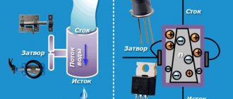
Why is a field effect transistor?
The word “transistor” is derived from two English words translate and resistor, that is, in other words, it is a resistance converter.
Among the variety of transistors, there are also field-effect ones, i.e. those that are controlled by an electric field.
An electric field is created by voltage. Thus, a field-effect transistor is a voltage-controlled semiconductor device.
In English literature the term MOSFET (MOS Field Effect Transistor) is used. There are other types of semiconductor transistors, in particular bipolar transistors, which are controlled by current. In this case, some power is also spent on control, since some voltage must be applied to the input electrodes.
The FET channel can be turned on by voltage alone, with no current flowing through the input electrodes (except for a very small leakage current). Those. no power is spent on control. In practice, however, field-effect transistors are mostly used not in static mode, but are switched at a certain frequency.
The design of the field-effect transistor determines the presence of an internal transition capacitance, through which, when switching, a certain current flows, depending on the frequency (the higher the frequency, the greater the current). So, strictly speaking, some power is still spent on control.
Devices
Vacuum tubes
For vacuum tubes, transconductance is defined as the change in plate (anode) current divided by the corresponding change in grid/cathode voltage, with a constant voltage between the plate (anode) and cathode. Typical gm values for a small signal vacuum tube are from 1 to 10 millisiemens. This is one of the three characteristic constants of a vacuum tube, the other two being its gain μ (mu) and the plate resistance rп or rа. The van der Bijl equation defines their relationship as follows:
g m = μ r p { displaystyle g_{m} = { frac { mu} {r_{p)))} [1]
Field effect transistors
Likewise in FETs, and MOSFETs in particular, transconductance is the change in drain current divided by the small change in gate/source voltage, with the drain/source voltage being constant. Typical g m
for a weak-signal field-effect transistor from 1 to 30 millisiemens.
Using the Szychman–Hodges model, the curvature for a MOSFET can be expressed as (see MOSFET article):
g m = 2 I DV OV { displaystyle g_{m} = { frac {2I_{D)) {V_{ text {OV))))}
where am I
is the constant drain current at the bias point, and
V OV
is the overload voltage, which is the difference between the gate-source bias point voltage and the threshold voltage (i.e.
V OV
≡
V GS
-
V th
).[2]:p .
395, Eq. (5.45) The overload voltage (sometimes known as the effective voltage) is typically selected at approximately 70–200 mV for a 65 nm process node ( μD
≈ 1.13 mA/μm width) for
μm
gm .[ 3]:p. 300, table 9.2[4]:p. 15, §0127
In addition, the transconductance of the transition field-effect transistor is determined by the expression g m = 2 i DSS | V p | ( 1 − V g SV p ) { displaystyle g_{m} = { frac {2I_{DSS)) { left | {V_ {P}} right |}} left ({1 - { frac {V_ {GS}} {V_ { P}}}} right)} , where Vп is the cut-off voltage and IDSS is the maximum drain current.
Traditionally, the transconductance for FETs and MOSFETs given in the above equations is derived from each device's transmission equation using calculus. However, Cartwright[5] showed that this can be done without calculus.
Bipolar transistors
Um of bipolar small signal transistors vary widely, being proportional to the collector current. Its typical range is from 1 to 400 millisiemens. The change in input voltage is applied between base/emitter and the output is the change in collector current flowing between collector/emitter with constant collector/emitter voltage.
The transconductance of a bipolar transistor can be expressed as
g m = i CV T { displaystyle g_{m} = { frac {I_{C)){V_{T)))}
where iC
= DC collector current at the Q-point, and
VT
= thermal voltage, usually about 26 mV at room temperature.
For a typical current of 10 mA, gm
≈ 385 mS. Input impedance is the current gain. (β) is divided by the slope.
The output (collector) conductance is determined by the Early voltage and is proportional to the collector current. For most transistors operating in linear mode, it is well below 100 µS.
Field effect transistors. For dummies
Introduction
Now let's talk about field effect transistors. What can you assume from their name alone? Firstly, since they are transistors, they can be used to somehow control the output current. Secondly, they are supposed to have three contacts. And thirdly, their operation is based on a pn junction. What will official sources tell us about this?
Field-effect transistors
are active semiconductor devices, usually with three terminals, in which the output current is controlled using an electric field.
(electrono.ru)
The definition not only confirmed our assumptions, but also demonstrated a feature of field-effect transistors - the output current is controlled by changing the applied electric field, i.e. voltage. But for bipolar transistors, as we remember, the output current is controlled by the input base current. Another fact about field-effect transistors can be learned by paying attention to their other name - unipolar
. This means that only one type of charge carrier (either electrons or holes) is involved in the process of current flow.
The three contacts of field effect transistors are called source
(source of current carriers),
gate
(control electrode) and
drain
(electrode where carriers flow).
The structure seems simple and very similar to the design of a bipolar transistor. But it can be implemented in at least two ways. Therefore, a distinction is made between field-effect transistors with a control pn junction
and
with an insulated gate
.
In general, the idea of the latter appeared back in the 20s of the 20th century, long before the invention of bipolar transistors. But the level of technology made it possible to implement it only in 1960. In the 50s, a field-effect transistor with a control pn junction was first theoretically described and then implemented. And, like their bipolar “brothers,” field-effect transistors still play a huge role in electronics.
Before moving on to the story about the physics of the operation of unipolar transistors, I would like to remind you of the links where you can refresh your knowledge about the pn junction: one and two.
Field effect transistor with control pn junction
So, how does the first type of field-effect transistor work? The device is based on a semiconductor plate with (for example) p-type conductivity. At the opposite ends it has electrodes, by applying voltage to which we will receive current from source to drain. On top of this plate there is an area with the opposite type of conductivity, to which the third electrode is connected - the gate. Naturally, a pn junction occurs between the gate and the p-region below it ( channel
).
And since the n-layer is significantly adjacent to
the same channel, most of the transition region depleted of mobile charge carriers will fall on the p-layer. Accordingly, if we apply a reverse bias voltage to the junction, then when it closes, it will significantly increase the channel resistance and reduce the current between source and drain. Thus, the output current of the transistor is regulated using the voltage (electric field) of the gate.
The following analogy can be drawn: a pn junction is a dam that blocks the flow of charge carriers from source to drain. By increasing or decreasing the reverse voltage on it, we open/close the gateways on it, regulating the “water supply” (output current).
So, in working mode
field-effect transistor with a control pn junction, the voltage at the gate must be either zero (the channel is fully open) or reverse.
If the reverse voltage becomes so large that the blocking layer closes the channel, the transistor will go into cutoff mode
.
Even with zero gate voltage, there is a reverse voltage between gate and drain equal to the source-drain voltage. This is why the pn junction has such a jagged shape, widening towards the drain region.
It goes without saying that it is possible to make a transistor with an n-type channel and a p-type gate. The essence of his work will not change.
Conventional graphic images of field-effect transistors are shown in the figure ( a
- with a p-type channel,
b
- with an n-type channel). The arrow here indicates the direction from the p-layer to the n-layer.
Static characteristics of a field-effect transistor with a control pn junction
Since in operating mode the gate current is usually small or even zero, we will not consider graphs of the input characteristics of field-effect transistors. Let's go straight to the weekend or stock. By the way, they are called static because a constant voltage is applied to the gate. Those. there is no need to take into account frequency moments, transients, etc.
The output
(
drain
) is the dependence of the drain current on the source-drain voltage at a constant gate-source voltage.
The figure shows the graph on the left.
Three zones can be clearly distinguished on the graph. The first of them is the zone of sharp increase in drain current. This is the so-called "ohmic" region
. The source-drain channel behaves like a resistor whose resistance is controlled by the voltage at the transistor's gate.
The second zone is the saturation region
. It has an almost linear appearance. Here, the channel overlaps in the drain region, which increases with a further increase in the source-drain voltage. Accordingly, the channel resistance also increases, and the drain current changes very little (Ohm's law, however). It is this section of the characteristic that is used in amplification technology, since here there is the least nonlinear signal distortion and optimal values of small-signal parameters that are essential for amplification. These parameters include slope, internal resistance and gain. The meanings of all these obscure phrases will be revealed below.
The third zone of the chart is the breakout area
, whose name speaks for itself.
On the right side of the figure there is a graph of another important relationship - the drain-gate characteristic
. It shows how the drain current depends on the gate-source voltage when the voltage between the source and drain is constant. And it is its steepness that is one of the main parameters of a field-effect transistor.
Insulated gate field effect transistor
Such transistors are also often called MOS (metal-dielectric-semiconductor) or MOS (metal-oxide-semiconductor) transistors (metal-oxide-semiconductor field effect transistor, MOSFET).
In such devices, the gate is separated from the channel by a thin layer of dielectric. The physical basis of their work is the effect of changing the conductivity of the near-surface layer of a semiconductor at the interface with a dielectric under the influence of a transverse electric field. The structure of transistors of this type is as follows. There is a semiconductor substrate with p-conductivity, in which two heavily doped regions with n-conductivity (source and drain) are made. Between them lies a narrow near-surface bridge, the conductivity of which is also n-type. Above it, on the surface of the wafer, there is a thin layer of dielectric (most often made of silicon dioxide - hence, by the way, the abbreviation MOS). And on this layer the shutter is located - a thin metal film. The crystal itself is usually connected to the source, although it happens that it is connected separately. If a source-drain voltage is applied at zero gate voltage, then current will flow through the channel between them. Why not through the crystal? Because one of the pn junctions will be closed.
Now let’s apply a voltage negative relative to the source to the gate. The resulting transverse electric field will “push” electrons from the channel into the substrate. Accordingly, the channel resistance will increase and the current flowing through it will decrease. This mode, in which the output current decreases as the gate voltage increases, is called depletion mode.
.
If we apply a voltage to the gate, which will contribute to the appearance of a field that “helps” electrons “come” into the channel from the substrate, then the transistor will operate in enrichment mode
. In this case, the resistance of the channel will drop, and the current through it will increase.
The design of a transistor with an insulated gate discussed above is similar to the design with a control pn junction in that even with zero current on the gate and a non-zero source-drain voltage, there is a so-called initial drain current
.
In both cases, this is due to the fact that the channel for this current is built
into the transistor design.
That is, strictly speaking, we have just considered such a subtype of MOS transistors as transistors with a built-in channel
.
However, there is another type of field-effect transistors with an insulated gate - an induced (inverse) channel transistor
. From the name it is already clear that it differs from the previous one - its channel between the heavily doped areas of the drain and source appears only when a voltage of a certain polarity is applied to the gate.
So, we only apply voltage to the source and drain. No current will flow between them, since one of the pn junctions between them and the substrate is closed. Let's apply voltage to the gate (direct relative to the source). The resulting electric field will “pull” electrons from the heavily doped regions into the substrate in the direction of the gate. And when the gate voltage reaches a certain value in the near-surface zone, a so-called inversion
type of conductivity. Those. the electron concentration will exceed the hole concentration, and a thin n-type channel will appear between the drain and source. The transistor will begin to conduct current, the stronger the higher the gate voltage. From this design it is clear that a transistor with an induced channel can only operate when in enrichment mode. Therefore they are often found in switching devices.
The symbols for insulated gate transistors are as follows:
Here a
− with built-in n-type channel;
b
– with a built-in p-type channel;
c
– with output from the substrate;
g
– with an n-type induced channel;
d
– with an induced p-type channel;
e
- with output from the substrate.
Static characteristics of MOS transistors
The drain family and drain-gate characteristics of a transistor with a built-in channel are presented in the following figure:
The same characteristics for a transistor with an induced channel:
Exotic MIS structures
In order not to confuse the presentation, I just want to recommend links where you can read about them. First of all, this is everyone’s favorite Wikipedia, the section “Special Purpose MDP Structures”. And here is the theory and formulas: textbook on solid-state electronics, chapter 6, subchapters 6.12-6.15. Read it, it's interesting!
General parameters of field-effect transistors
- Maximum drain current
at a fixed gate-source voltage. - The maximum drain-source voltage
, after which breakdown occurs. - Internal (output) resistance
. It represents the channel resistance for alternating current (gate-source voltage is constant). - Slope of the drain-gate characteristic
. The larger it is, the “sharper” the transistor’s response to changes in gate voltage. - Input impedance
. It is determined by the resistance of the reverse-biased pn junction and usually reaches several and tens of megohms (which distinguishes field-effect transistors from their bipolar “relatives”). And among the field-effect transistors themselves, the palm belongs to devices with an insulated gate. - Gain
is the ratio of the change in source-drain voltage to the change in gate-source voltage at a constant drain current.
Connection schemes
Like a bipolar one, a field-effect transistor can be considered as a four-terminal device, in which two of the four contacts coincide. Thus, three types of switching circuits can be distinguished: with a common source, with a common gate and with a common drain. Their characteristics are very similar to common emitter, common base, and common collector circuits for bipolar transistors. Most often, a circuit with a common source
(
a
) is used, as it gives greater current and power gain.
A circuit with a common gate
(
b
) provides almost no current amplification and has a low input resistance.
Because of this, such a connection scheme has limited practical application.
A
common drain circuit
is also called
a source follower
. Its voltage gain is close to unity, the input impedance is high and the output impedance is low.
Differences between field-effect transistors and bipolar ones. Areas of use
As mentioned above, the first and main difference between these two types of transistors is that the latter are controlled by changing the current, and the former by voltage. And from this follow other advantages of field-effect transistors compared to bipolar ones:
- high input impedance for direct current and at high frequency, hence low control losses;
- high performance (due to the absence of accumulation and resorption of minor carriers);
- since the amplifying properties of field-effect transistors are due to the transfer of majority charge carriers, their upper limit of effective gain is higher than that of bipolar ones;
- high temperature stability;
- low noise level, since field-effect transistors do not use the phenomenon of injection of minority charge carriers, which makes bipolar transistors “noisy”;
- low power consumption.
However, with all this, field-effect transistors also have a drawback - they are “afraid” of static electricity, therefore, when working with them, they have particularly stringent requirements for protection from this scourge.
Where are field-effect transistors used? Yes, almost everywhere. Digital and analog integrated circuits, tracking and logical devices, energy-saving circuits, flash memory... Why, even quartz clocks and TV remote control work on field-effect transistors. They are everywhere, % habrowser
%. But now you know how they work!
List of sources:
ru.wikipedia.org dssp.petrsu.ru zpostbox.narod.ru electrono.ru radio.cybernet.name
Helpful comments:
https://habrahabr.ru/blogs/easyelectronics/133493/#comment_4435883 https://habrahabr.ru/blogs/easyelectronics/133493/#comment_4436509 https://habrahabr.ru/blogs/easyelectronics/133493/#comment_4441531
I recommend reading:
“Basics on your fingers”, author DI HALT (thanks to AlexeiKozlov for the tip)
Amplifiers
Coolness boosters
And the steepness amplifier
(
gm
amplifier) produces a current proportional to its input voltage.
In network analysis
, a transconductor amplifier is defined as
a voltage controlled current source
(
VCCS
). Typically these amplifiers are installed in a cascode configuration that improves frequency response.
Resistance Amplifiers
Main article: transimpedance amplifier
A resistance amplifier
outputs a voltage proportional to the input current.
An impedance amplifier is often referred to as a transimpedance amplifier
, especially by semiconductor manufacturers.
Term for resistance amplifier in network analysis: current controlled voltage source
(
CCVS
).
A basic inverting resistance amplifier can be built from an op-amp and a single resistor. Simply connect a resistor between the output and the inverting input of the op-amp and connect the non-inverting input to ground. Then the output voltage will be proportional to the input current at the inverting input, decreasing as the input current increases and vice versa.
To amplify the signal current from photodiodes at the receiving end of ultra-high-speed fiber optic lines, special transresistor (transimpedance) amplifier microcircuits are widely used.
Transconductance operational amplifiers
An operational transconductance amplifier (OTA) is an integrated circuit that can work as a transconductance amplifier. They usually have an input that allows you to control the slope.[6]
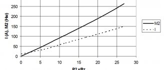
Output (drain) characteristics of the transistor
The output characteristic is called a dependence of the form ic=f(uis)|uzi =const where f is a certain function.
Let us depict the output characteristics for a silicon transistor of the KP10ZL type with a pn junction and a p-type channel (Fig. 1.90).
Let us turn to the characteristic corresponding to the condition uzi = 0. In the so-called linear region (uis < 4 V) the characteristic is almost linear (all characteristics of this region are almost straight lines fan-shaped from the origin). It is determined by the channel resistance. A transistor operating in the linear region can be used as a linear controlled resistor.
Abrahamyan Evgeniy Pavlovich
Associate Professor, Department of Electrical Engineering, St. Petersburg State Polytechnic University
Ask a Question
At ui = 3 V, the channel in the drain area is blocked. A further increase in voltage leads to a very slight increase in current ic, since with increasing voltage the region in which the channel is blocked (characterized by a very high resistivity) expands. In this case, the DC resistance of the source-drain gap increases, but the current ic remains virtually unchanged.
The drain current in the saturation region at uzi = 0 and at a given voltage uis is called the initial drain current and is denoted by ic init. For the characteristics under consideration, ic initial = 5 mA at ui = 10 V. For a transistor of the KP10ZL type, the minimum current value ic is initially 1.8 mA, and the maximum is 6.6 mA. At uis > 22 V, a breakdown of the pn junction occurs and a rapid increase in current begins.
Now we will briefly describe the operation of the transistor at various voltages. The higher the specified voltage uis, the thinner the channel before applying voltage uis and the lower the characteristic is located.
As is easy to see, in the drain region the voltage at the pn junction is equal to the sum uzi + uis. Therefore, the greater the voltage uzi, the lower the voltage uis corresponding to the onset of breakdown.
When uzi = 3 V, the channel is blocked by the pn-junction region even before voltage uis is applied. In this case, before breakdown, the condition ic = 0 is satisfied. Thus, uzi otc = 3 V. For the type of transistor under consideration, the minimum cutoff voltage is +2 V, and the maximum is +5 V. These values correspond to the condition ic = 10 μA. This is the so-called residual drain current, which is denoted by ic ots. The field-effect transistor is characterized by the following limit parameters (the meaning of which is clear from the notation): uis max, uzsmax, Pmax.
For the KP10ZL transistor uismax = 10 V, uzsmax = 15 V, Pmax = 120 mW (all at t = 85°C).
References
- Blencowe, Merlin (2009). "Development of tube amplifiers for guitar and bass."
- Sedra, A.S.; Smith, K. (1998), Microelectronic Circuits
(Fourth ed.), New York: Oxford University Press, ISBN 0-19-511663-1 - Baker, R. Jacob (2010), CMOS Circuit Design, Layout, and Simulation, Third Edition
, New York: Wiley-IEEE, ISBN 978-0-470-88132-3 - Sansen, W. M. C. (2006), Fundamentals of Analog Design
, Dordrecht: Springer, ISBN 0-387-25746-2 - Cartwright, Kenneth V (Fall 2009), "Deriving the exact transconductance of a field-effect transistor without calculus" (PDF), Technology Interface Magazine
,
10
(1): 7 pages - "3.2 Gbps SFP Transimpedance Amplifiers with RSSI" (PDF). datasheets.maximintegrated.com
. Maksim. Retrieved November 15, 2022.
- Horowitz, Paul & Hill, Winfield (1989), The Art of Electronics
, Cambridge University Press, ISBN 0-521-37095-7 CS1 maint: multiple names: authors list (site link)
Graphical analysis of circuits with field-effect transistors.
To better understand the operating principle of circuits with field-effect transistors, it is useful to conduct a graphical analysis of one of them (Fig. 1.91).
Let Ec = 4 V; Let us determine within what limits the voltage u will change when the voltage ui changes from 0 to 2 V.
Graphical analysis uses the same approach that was used when analyzing circuits with diodes and bipolar transistors. For the circuit under consideration, in which the voltage between the gate and the source is equal to the voltage of the voltage source uzi, there is no need to build a load line for the input circuit. The load line for the output circuit is given by the expression Ес =iс·Rс+uiс Let's construct a load line on the output characteristics of the transistor shown in Fig. 1.92.
It follows from the figure that with the above change in voltage u, the voltage uis will vary from 1 to 2.6 V, which corresponds to the movement of the initial operating point from point A to point B. In this case, the drain current will change from 1.5 to 0, 7 mA.
Vasiliev Dmitry Petrovich
Professor of Electrical Engineering, St. Petersburg State Polytechnic University
Ask a Question
Gate characteristics (transmission characteristics, transfer, transient, pass-through characteristics). The drainage characteristic is called a dependence of the form ic=f(uzi) |uis =const where f is a certain function.
Such characteristics do not provide fundamentally new information compared to weekend ones, but are sometimes more convenient to use. Let us depict the drain gate characteristics for the KP10ZL transistor (Fig. 1.93).
For some transistors, the maximum (modulo) permissible negative voltage uzi is set, for example, for the 2P103D transistor this voltage should not be more than 0.5 V in modulus.