Photodiodes are ordinary semiconductor diodes, but they convert light into electricity. These are the same solar batteries, as well as elements that respond to light in a variety of relays, sensors, microcircuits, and especially in fiber optic systems, equipment related to light (UV, IR), its intensity. In these same areas, LEDs, phototransistors, and photoresistors are used, but they and the drawings for them should be distinguished. We will describe what a photodiode is, how it functions, its types, its components, how it is included in assemblies and on device boards, and we will also describe circuits with these radio components.
Photodiode concept
A photodiode, PD, is a semiconductor part, the same diode as it passes current in one direction, with a pn (pin) junction, but from a material that changes its qualities under the influence of optical radiation, initiating processes that create electric current.
If the light is completely absent and does not fall on such a radio component, then in a calm state, in equilibrium, it has qualities similar to a simple diode.
If UV or IR radiation hits a sensitive area, the element begins to react, converting this flow into electricity.
It is necessary to distinguish between different radio components with the prefix “photo”:
- the photodiode we are considering. The essence of a “photo” or “opto”, “galvanic” (such names are used less frequently) diode, which immediately distinguishes it, can be briefly expressed in one sentence: the part converts light into current;
- phototransistors. “Two in one” is a photocell and a transistor combined in one housing, which opens depending on the amount of light supplied. That is, if in the diagrams we discussed below these elements are separated, then in this case they are in the same crimp. Instead of a bunch of individual specified parts, you can use such a one-piece spare part if it fits the parameters;
- photoresistors. They change the resistance (this is the key parameter here) depending on the light level.
As you can see, “photo” radio components can be used for very similar, in some cases similar purposes (for example, sensors, relays), but the circuits will be different, taking into account the differences in the operating principle of each type.
You also need to know the designation of different elements on the diagrams. The photodetector has two arrows directed towards it, and there is logic in such graphics: the product perceives radiation.
The LED often cooperates in circuits with a photodiode. The first initiates the operation of the second: it is placed opposite, and when turned on, a stream of light falls on the first element, activates it, and it sends a signal to the actuator unit. This principle is used for remote controls, various IR signal receivers, as well as for optical (laser) alarms that are activated if the light stream is crossed by an intruder.
So, the photocell converts the light falling on its sensitive segment into an electrical charge. This process occurs due to the occurrence of special processes during the movement of charge transporter particles at the atomic level during irradiation of the pn zone. This phenomenon is caused by changes in the properties of the materials used (semiconductors).
If on photoresistors it is the conductivity that changes when the charge transporters move, then on photodiodes a current appears at the closing segments of the pn junctions - this is their difference.
Structure
A regular LED has the same structure as a “photo”, but the latter has a window so that the light falls on the part that receives it.
Photodiode structure diagram:
Associated devices
Avalanche photodiodes
photodiodes with a structure optimized for operation with high reverse bias, approaching the reverse breakdown voltage.
This allows each photo generated
carrier to be multiplied by the avalanche, resulting in an internal gain of the photodiode that increases the effective
responsiveness
of the device.
Electronic symbol for phototransistor
A phototransistor
is a light-sensitive transistor.
A common type of phototransistor, the bipolar phototransistor
, is essentially a bipolar transistor enclosed in a transparent case so that light can reach
the base-collector junction
.
It was invented by Dr. John N. Shive (better known for his wave machine) at Bell Labs in 1948[5]:205 but this was not announced until 1950.[6] Electrons that are generated by photons at the base-collector junction are injected into the base, and this photodiode current is amplified by the transistor's current gain β (or hfe). If the base and collector terminals are used and the emitter is left unconnected, the phototransistor becomes a photodiode. While phototransistors have higher responsiveness When it comes to light, they cannot detect low levels of light better than photodiodes.[ citation needed
] Phototransistors also have significantly faster response times.
Another type of phototransistor, a photofield-effect transistor
(also known as a photoFET) is a light-sensitive field-effect transistor. Unlike photobipolar transistors, photovoltaic transistors control drain-source current to produce a gate voltage.
And the solaristor
It is a two-terminal phototransistor without a gate. A compact class of bipolar phototransistors or solaristors was demonstrated in 2022 by ICN2 researchers. The new concept is a two-in-one power supply and transistor powered by solar energy by exploiting the memresistive effect in a stream of photogenerated carriers.[7]
Principles of operation of photodiodes
We will try to describe as clearly as possible, in simple words, the principle of operation, the properties of the photodiode, how it functions, how electric particles move and interact with the pn sections:
- In the figure below there is a semiconductor: on the left is the p-variant, on the right is n. On the first, the number of “holes” (they are also positively charged electrons) is excessive, on the second, there is an excessive number of free electrons.
- Diffusion occurs - holes penetrate into segment n, electrons penetrate into segment p. The remaining particles pass through, forming a barrier layer that prevents the movement of the first and second.
- If voltage is applied: “+” on the left, “−” on the right, then current will flow as the blocking layer will be overcome. When voltage is applied, on the contrary, this layer will become large, the current value will be very small, approaching or equaling zero.
- The photosensitive location of the photocell is n. If this segment is darkened, then its behavior is similar to a conventional diode. When light or electromagnetic waves hit it, electrons are knocked out of the outer layers of the atoms. Their number and holes (together these are photocarriers) increases, the particles diffuse in different directions (towards the contacts of the part - anode, cathode). At the pn junction, holes are transmitted, but electrons are retained. A potential difference, an electric current, appears.
This is what the diode looks like in a quiet state:
More complex explanation:
- The radiation is directed perpendicular to location pn. The energy at which photons are absorbed becomes greater than the band gap, and electron-hole pairs—photocarriers—are formed;
- When phototransporters penetrate into the n-region, most of them (not all) do not have time to break up into components and end up close to the boundary of the pn region, where they are separated by an electric field;
- In the described process, holes end up on the p-segment, but electrons cannot penetrate the field enveloping the transition, so they accumulate near the n-region and at the edge of the transition.
- The particles each move towards their own electrode, thus a current arises; its flow through the junction is completely dependent on the movement of holes; this version of it (in which photocarriers participate) is called drift current or photocurrent.
You can very briefly express how a photodiode generates current as follows. A consequence of the concentration of holes and electrons at p and n locations, respectively, is the formation of a potential difference. The same phenomenon is an electromotive force that creates a reverse current, cathode⇒anode, and in the external circuit it will be the other way around. This is a solar (helio) electric panel (battery).
Photodiode modes
Applications and types of photodiode have their own nuances depending on the mode for which it is used.
There are two main modes based on the method of using the process of converting radiation into current:
- photovoltaic (generator) - these are the same solar panels. Small ones are used for calculators, stand-alone lamps and the like. Large ones - for autonomous systems for providing electricity to houses, cars and other things. These are power sources;
- photodiode (converter). With external reverse voltage. For controlling various devices. For example, for lighting with automatic shutdown after sunrise. In the absence of radiation, the element is an ordinary diode, it passes current, but during the day it blocks the flow.
In converter mode, the part acts as a light-controlled switch, for which it is connected to the circuit in forward bias - with the cathode to “+” and the anode to “−”. In the dark there is only reverse, dark current (Irev, units and tens of μA). In light, a photocurrent is added to this, depending only on the intensity of the radiation (tens of μA); the stronger the radiation, the more powerful it is.
The photocurrent is calculated by the formula: Iф=Sint×Ф. Where the first component is the integral sensitivity, the second is the luminous flux.
How do the two photodiode modes differ?
In converter mode, the diode is biased in the reverse direction by voltage. The photocurrent that appears under illumination is at the same time a function of the power of the luminous flux. With a generator, the part creates a photoEMF. In other words, when radiation hits the pn junction, a voltage proportional to the flux intensity appears at the output of the element.
The photodiode (converter) operating algorithm is more often used for prompt powering of devices. Its advantages: higher performance, greater sensitivity to optical radiation, wider dynamic range. But there is a significant disadvantage - there is a noise current flowing through the load. Sound effects are reduced by cooling the part to −10° C, but this is expensive. Sometimes because of this, when there is a need for absence of noise, preference is given to the galvanic (photovoltaic) operating algorithm
When using the conversion algorithm, the power source is connected with reverse polarity, here the purpose of the photodetector is to act as a light sensor.
Operating modes
Photodiodes are divided according to their operating mode.
Photo generator mode
Performed without a power source. Photogenerators that are components of solar batteries are otherwise called “solar cells”. Their function is to convert solar energy into electrical energy. The most common photogenerators are based on silicon - cheap, widespread, and well studied. They have a low cost, but their efficiency reaches only 20%. Film elements are more progressive.
Photoconversion mode
The power supply is connected to the circuit with reverse polarity; the photodiode in this case serves as a light sensor.
Characteristics of photodiodes for selection
Photodiode parameters can be found in their specifications online. Let's look at the items by which parts are selected. It should be said that for simple purposes (light relay, IR receiver), the characteristics listed below can be ignored; it is enough to buy the recommended product for a specific assembly.
Current-voltage qualities that determine changes in luminous flux values according to changing voltage with a stable radiation flux and dark current. Below is a standard I-V diagram of a photodiode.
Spectral qualities (sensitivity). They display how the wavelength of light and the angle of incidence of the rays change the characteristics of the photocurrent on different semiconductors.
Sensitivity can be measured under different light parameters:
Light or energy characteristic. Explained in the picture below:
Temporary constant. The period during which the current responds to an increase/decrease in dimming or illumination by 63% of the set value.
Lower limit of sensitivity. Minimum light intensity for a photodiode reaction to occur.
Dark resistance. Characterizes the state of the semiconductor in the absence of light; this is the current-voltage characteristic in the absence of radiation.
Inertia:
The above main characteristics are used to select photodiodes for load parameters:
Applications of photodiodes
- Optoelectronic integrated circuits. Semiconductors provide optical communication, which ensures efficient galvanic isolation of power and control circuits while maintaining functional communication.
- Multi-element photodetectors - scanistors, photosensitive devices, photodiode matrices. The optoelectric element is capable of perceiving not only the brightness characteristics of an object and its change over time, but also creating a complete visual image.
Other areas of use: fiber optic lines, laser range finders, positron emission tomography installations.
Options, types of photodetectors
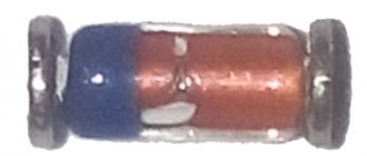
The infrared photodiode is made in a black housing and reacts only to IR radiation. The dark color of the lens is a kind of filter tint so as not to interfere with other spectrums.
Photodetectors have a frequency range, here it is orders of magnitude larger, up to 10 MHz (much higher than that of photoresistors), which ensures excellent performance. For pin variants and with a Schottky barrier this figure is 100 MHz–1 GHz, for avalanche variants it is 1–10 GHz.
We will consider the types of photodiodes based on their operating principle, combination options, placement of layers, and materials below.
Photodiode pin
Pin-type elements are widely used for fiber-optic communication systems - they convert light into electrical signals, which are then converted into information (video, sound, etc.)
The p and n layers are made using doping: impurities that enhance it are added to the semiconductor material. If there is a + in the designation of such a part, then this indicates an increased content of additives.
The middle segment - part "i" - is the conductor "n", but lightly alloyed. If a reverse voltage is applied to it, then a depleted location is formed there (there are fewer holes/electrons).
The resistance on the i-segment increases, much higher than that on p+ and n+. The result of this process: the electric field is concentrated in the i-region, the photon absorbed there creates a pair: electron/hole. A powerful field in the i-section instantly distributes them to the electrodes: the hole is absorbed by the cathode, the electron by the anode. This creates an electric current.
The efficiency of pin photodiodes is extremely high, since their frequency can reach 1010 Hz, which guarantees the transfer of terabytes of data in 1 second. For such parts, the i-section is much wider than the p+ and n+ so that photons are absorbed more precisely in this segment.
Avalanche
In fiber optic technologies, in addition to the pin types of the parts under consideration, special types are used - avalanche photodetectors (APDs), their difference is an additional p-section.
Due to the reinforcing additives, the p-layer has a higher resistance and, accordingly, the greatest decrease in voltage across it. The photon, finding itself in the light-sensitive i-segment, pulls out an electron from there, rushing to the anode, the hole goes to the cathode.
On its route, the electron ends up at a location of high voltage in the p-layer, here it accelerates sharply, which allows it to knock other similar particles out of the shells of the atoms of the p-section. Then the newly formed free electrons do the same - they knock out additional analogues from the valence segments. The phenomenon is growing like an avalanche.
The image visualizes a sharp surge in the driving electric force on the p-layer. The primary current that appears in the i-layer grows like an avalanche in the p-section. The increase reaches several hundred times, but if it is too large, it creates noise that increases faster than the pulse. The optimal coefficient value is 30–100.
With Schottky barrier
In this type of element, several films are created, that is, a special structure that allows one to avoid the injection of minority carriers. Such parts use the movement of only the main transporters. The advantage is that there are no slow processes influenced by the phenomena of accumulation and resorption of secondary carriers based on the diode. Pros: inertia, recharging times are negligible, the first is determined only by the time of passage of carriers through the space charge regions.
The above abilities allow the use of optodiodes for microwave modulation of radiation.
Heterostructural
They are assembled from 2 semiconductors with different sizes of the forbidden segment; the section between them is called heterogeneous. A special selection of materials is used to create a device that covers (perceives) the full extent of the waves. The disadvantage of such a product is the cost of production.
Electronic educational and methodological complex on TM and ABOUT TsVOSP
Operating principle, main characteristics.
A pin photodiode is characterized by the presence of an i-layer (a lightly doped n-type semiconductor) between the p+ (base) and n+ (collector) layers (+ means heavy doping).
The i-layer is also called the depletion layer. Photons are introduced into the detector through a window having a thin layer of antireflection coating (thickness about λ /4) with a refractive index that matches different media - glass fiber (n = 1.46) and semiconductor (n = 3.5).
A reverse bias (-U cm) is applied to such a diode, i.e. voltage is plus to the n-junction, minus to the p-junction.
Heavy doping of the outer layers makes them conductive, and the maximum value of electric current is created in the i-layer. But since there are no free carriers in the i-layer, there is no electric current or radiation on the i-layer, free electron-hole pairs are formed in it. Under the influence of an electric field, these pairs quickly separate and move in opposite directions towards their electrodes.
Thus, a photocurrent (drift current) is created.
I f
= Ne × Q
where Q
— electron charge;
Ne
– number of electrons
However, not all photons cause the formation of electron-hole pairs. For this reason, the concept of quantum efficiency is introduced. Quantum efficiency q (dimensionless quantity) is defined as:
where N f
— the number of photons falling per unit time on the receiver;
Ne
— the number of free electrons (or electron-hole pairs) generated as a result.
Quantum efficiency for pin photodiodes cannot be higher (100%)
The photocurrent value is determined:
I f =
N f ∙η∙e
Considering that the number of photons depends on the radiation power
,
where is Eph
= h∙v, and λ = C/v, then the photocurrent value can be represented:
where Ri is the total optical power of radiation at wavelength λ incident on the photosensitive area (W);
e—electron charge (1.6∙C);
h is Planck’s constant, eVˑs (see above);
C is the speed of light in emptiness (air), (C = 3∙ m/s);
η
— quantum efficiency.
The interaction of radiation only with the i layer is effective, since when photons enter the p+ and n+ layers, a diffusion current appears, which has a large inertia and worsens performance. Therefore, when manufacturing photodiodes, they strive to make the p+ and n+ layers as thin as possible, and the depletion region is large enough so that it completely absorbs all the incident light. Figure 1.21 shows the structure, connection and potential distribution of the pin photodiode.
There are several types of photodetectors that can be used as light receivers in FOTS. However, only two of them are most attractive for broadband WWTP. These are silicon pin photodiodes and InGaAs* pin photodiodes. Silicon photodiodes can be used in applications operating in the short wavelength range (850 nm), while InGaAs photodiodes can be used in applications operating in the long wavelength range of 1310 and 1550 nm.
Figure 1.21. Structure, switching on and potential distribution of pin photodiode
Characteristics of pin photodiodes
When choosing a photodetector for fiber-optic lines, they are compared according to a number of characteristics:
The quantum efficiency of a photodiode, η, is a measure of the average number of electrons released by each incident photon.
When operating under ideal conditions of reflection, crystal structure and internal resistance, optimally designed high-quality silicon photodiodes are capable of achieving quantum efficiencies in the order of 80%. Quantum efficiency of 100% is unattainable.
Quantum efficiency curves as a function of wavelength for various materials are shown in Figure 1.22.
Response sensitivity is the most important parameter when working with photodiode detectors. Response sensitivity is expressed in A/W (current sensitivity) or V/W (voltage sensitivity) and is sometimes simply called sensitivity or integral sensitivity.
Figure 1.22. Dependence of quantum efficiency on wavelength for various materials
Response sensitivity is the ratio of the root mean square (RMS) value of the output current or voltage of the photodetector to the root mean square (RMS) value of the electrical power, i.e.:
,
where Iph is the photocurrent, and Ri is the total optical power of radiation at wavelength λ incident on the photosensitive area.
For a photodiode, the response sensitivity S is related to the wavelength of the light flux A and the quantum efficiency q, the fraction of incident photons that produce electron-hole pairs. Hence,
,
where λ is the radiation wavelength, nm;
η
— quantum efficiency.
The sensitivity of the response can also be related to the charge of the electron by the following expression:
where η
— quantum efficiency;
e - electron charge (1.6*1019 C);
h is Planck’s constant, eV-s (see above);
ν
— radiation frequency in Hz.
The typical value of current sensitivity for pin photodiodes in their operating ranges is 0.5...0.8 A/W.
The spectral characteristic reflects the dependence of the sensitivity of the photodetector on the wavelength of the acting monochromatic radiation S = f(λ). This characteristic determines the spectral range of application of the photodetector.
Figure 1.23. Spectral characteristics of germanium (1) and silicon (2) photodiodes.
The range of spectral sensitivity depends on the material from which the photodiode is made. Typical spectral characteristics of photodiodes are shown in Figure 1.23.
The dependence of spectral sensitivity on wavelength is complex. This dependence has a maximum at a certain wavelength (λ 0), and the decrease in the region of long waves is associated with the dependence of the quantum yield η
(λ) on the wavelength, and in the region of short wavelengths - with the dependence of the interband absorption coefficient a(λ) on the wavelength. The absorption coefficient increases and most of the radiation is absorbed in the surface layer of the base and a smaller part of the carriers generated by the light reaches the p-n junction. That is, the position of the short-wavelength photosensitivity boundary depends on the base width and the surface recombination rate. Both dependences have a red boundary, since when the photon energy hv is less than the band gap Eg, interband absorption of light does not occur.
Dark current It (A) flows under reverse bias through the load in the absence of radiation incident on the photodiode. Its value depends on the semiconductor material, ambient temperature, and the design of the photodetector. This current has maximum values in photodiodes made of germanium and ranges from fractions to units of milliampere.
Volt is the ampere characteristic of the photodiode. The volt-ampere characteristic reflects the dependence of the current I passing in the photodetector circuit on the voltage U across it at a given radiation flux
I = f(U).
The light (total) current is the sum of the currents:
I = IT + I f ,
where IT is the current in the absence of lighting; Iph - photocurrent.
Figure 1.24 shows circuits for connecting a photodiode with a resistor Rн.
| — + |
| F |
| Rн |
| Ucm |
| I |
Figure 1.24. Schemes for connecting a photodiode with a resistor Rн:
a) circuit diagram for switching on the PD in photodiode mode,
b) circuit diagram for switching on the PD in photovoltaic mode
Figure 1.25 shows the family of volt-ampere characteristics of a p-in photodiode. The value Unp is the electrical breakdown voltage of the photodiode.
The volt-ampere characteristics of the photodiode in quadrant I correspond to switching on in the forward direction.
If you open the PD, a direct current (diffusion current) will flow through it, significantly exceeding the photocurrent. Photocontrol of the current through the diode becomes impossible (quadrant I is the non-working area for the photodiode).
Quadrant II reflects operation in photovoltaic mode. Along the voltage axis, it is possible to determine the photo-emf (Uхх) at different intensities of the received light flux Ф and at Rн =∞. The points of intersection of the volt-ampere characteristics with the current axis correspond to the values of short-circuit photocurrents Is.c. (Rн = 0). Intermediate values of load resistance are determined by load lines, which for different values of R leave the origin coordinates at different angles. For a given current value according to the volt-ampere characteristic, you can select the optimal mode of operation of the photodiode in the photovoltaic mode. In this case, the optimal mode is understood as the choice of such a load resistance at which the greatest electrical power will be transmitted to Rн.
Figure 1.25. Family of volt-ampere characteristics of a pin photodiode
If you open the PD, a direct current (diffusion current) will flow through it, significantly exceeding the photocurrent. Photocontrol of the current through the diode becomes impossible (quadrant I is the non-working area for the photodiode).
Quadrant II reflects operation in photovoltaic mode. Along the voltage axis, it is possible to determine the photo-emf (Uхх) at different intensities of the received light flux Ф and at Rн =∞. The points of intersection of the volt-ampere characteristics with the current axis correspond to the values of short-circuit photocurrents Is.c. (Rн = 0). Intermediate values of load resistance are determined by load lines, which for different values of R leave the origin coordinates at different angles. For a given current value according to the volt-ampere characteristic, you can select the optimal mode of operation of the photodiode in the photovoltaic mode. In this case, the optimal mode is understood as the choice of such a load resistance at which the greatest electrical power will be transmitted to Rн.
Quadrant III characterizes the device being turned on in photodiode mode (reverse voltage is applied to the p-n junction). In the operating range of reverse voltages, the photocurrent is practically independent of the reverse voltage of the load resistance.
The volt-ampere characteristic of the load resistor RH is a straight line.
Since the photodiode and load resistor are connected in series (see Fig. 24a), one current of 1N flows through them. This current can be determined by the intersection point of the volt-ampere characteristic of the photodiode and the load line of the resistor (quadrant III). Thus, in the photodiode mode, for a given radiation flux, the photodiode is a source of current in relation to the external circuit. The value of the current In practically does not depend on the parameters of the external circuit (UCM, RH).
The energy (light) characteristic displays the dependence of the photoresponse of the device on the intensity of the exciting radiation flux (ampere - watt I = f(F), volt - watt U = f(F), lux - ampere). The energy characteristic is also called the dependence of the integral or spectral sensitivity of the receiver on the intensity of the radiation flux. The energy characteristics of PDs in photodiode mode are linear over a wide range.
Frequency characteristics describe the dependence of sensitivity on the radiation modulation frequency or pulse duration and characterize the inertia of the device. Figure 1.26 shows the frequency response of the photodiode.
Figure 1.26. Photodiode frequency response
Photodiodes are low-inertia photodetectors. Their inertia depends on the capacitance of the pn junction, the conditions for the separation of electron-hole pairs and the load resistance. Optical communication lines require high-speed photo devices (several nanoseconds or less). Photodevices with low inertia include pi-n photodiodes and avalanche photodiodes.
The speed of the photodiode depends on the rise time of the photocurrent when the photodiode is exposed to an optical power pulse (Fig. 1.27).
Rise time trise (fall time tfall)
- this is the most important dynamic characteristic of a photodetector. It is defined as the time required for the output signal to rise from a level of 0.1 to 0.9 (fall from 0.9 to 0.1) from the steady-state maximum value, provided that strictly rectangular light pulses of long duration are supplied to the input. These times depend on the geometry of the photodiode, the material, the electric field strength in the lightly doped region, and temperature. The maximum of the two values (usually trise) is taken as a characteristic of the response time of the photodetector. As the modulation frequency of the input optical pulses increases, the maximum value of the phototek decreases. The limiting frequency is defined as the modulation frequency at which the current sensitivity is 0.707 of the current sensitivity value at low modulation frequencies (see Figure 1.26).
Figure 1.27. Performance characteristics of p-in PD
While internal delays do not directly affect bandwidth or bit rate, rise and fall times primarily determine bandwidth. Different photodetectors can vary greatly in performance. The fastest are p-i-n photodiodes.
The speed of the photodiode is determined by the carrier drift time through the i-region. Therefore, to increase performance, it is desirable to reduce the thickness of the i-layer for electric current and maintain the thickness for light flux. This is implemented in the design of a photodiode in the shape of a “mesa” - a mountain, which is presented in Figure 1.28.
Figure 1.28 Design of a mesa-shaped pin photodiode
— The maximum permissible reverse voltage Uob.max.additional is a voltage, the excess of which can lead to breakdown of the photodetector and its destruction. Along with this value or instead of it, manufacturers of photodetectors can simply indicate the reverse operating voltage. If you choose a lower value of the operating voltage, the area will be limited linear characteristic of the photodetector. The range of possible operating voltages of typical p-in photodiodes is Uwork = 1…30 V.
— Photodiode pin noise. When analyzing the noise properties of a photodetector, i.e., if it is necessary to find the signal-to-noise ratio or determine the sensitivity limited only by the photodetector, it is usually necessary to take into account three types of noise currents: 1) noise current arising when detecting a light flux (shot noise); 2) noise current caused by random thermal movement of electrons in the load resistance and in subsequent electronic circuits; 3) the noise current of the PD itself, the main component of which is due to the tempo current. Those. The photodiode current consists of three components:
Ifd = If+Ifon+It,
where Iph is the current due to signal detection,
Ibackground – current caused by extraneous (background) optical radiation entering the photodetector;
It is the tempo current.
If we reduce the thermal noise of the load resistance by changing the effective temperature of the resistance, and the fundamentally irremovable shot noise is considered small, then the threshold sensitivity of the PD will be determined by the new current. From this point of view, to achieve maximum threshold sensitivity, it is necessary to select PDs with minimal dark currents. The magnitude of the dark current depends on the properties of the PD material, temperature, pn junction area, design features, etc.
— The electrical circuit for switching on the photodiode is shown in Figure 1.29.
Figure 1.29. Pin photodiode connection circuit
In the switching circuit, the separating capacitance Cp allows you to eliminate the high bias voltage Ucm (up to 30 V) from the input of the low-noise amplifier.
— The dynamic range of linearity (in decibels) characterizes the range of values of the luminous flux Ф (from Фmin to Фmax), in which the energy (light) characteristic is linear:
∆ = 10lg∙(Фmax/Фmin).
The dynamic range of input optical powers for a photodiode circuit with an amplifier can reach ∆ pin - 60 dB.
Advantages and disadvantages of pin photodiode
The advantages of pin photodiodes include the following:
· high photosensitivity (for λ = 0.9 µm, Smax = 0.7 A/W) and high performance
· high photosensitivity in the long-wave part of the spectrum (due to the wide i - region);
· low barrier capacity;
· high efficiency at low reverse voltages.
The disadvantages of pin photodiodes include:
· low photo - emf (≤ 0.35 - 0.45 V);
· increased leakage currents;
· pin diodes are not compatible with ICs.
Checking the photodiode with a multimeter
Let's look at how to check photo detectors with a multimeter. The tester measures the resistance values (reverse and forward) during the process of lighting/darkening the diode. The multimeter (or ohmmeter) is set to 200 kOhm.
Sometimes a characteristic defect occurs - a chaotic change in current (“creep”). To detect a problem, assemble a simple circuit (see figure below) and measure the amount of reverse current for several minutes. If the current is constant, then the part is working. You can check the spare part on the board, but errors are possible, so desoldering is always recommended.
Photodiode array
2 x 2 cm photodiode array chip with over 200 diodes
A one-dimensional array of hundreds or thousands of photodiodes can be used as a position sensor, for example as part of an angle sensor.[23]
In recent years, one of the advantages of modern photodiode arrays (PDAs) is that they can provide high-speed parallel readout because the control electronics cannot be embedded as a charge-coupled device (CCD) or CMOS sensor.
Passive pixel sensor
A passive pixel sensor (PPS) is a type of photodiode array. It was the predecessor of the active pixel sensor (APS).[20] A passive pixel sensor consists of passive pixels that are read without amplification, where each pixel consists of a photodiode and a MOSFET switch.[24] In the photodiode array, the pixels contain a pn junction, an integrated capacitor, and MOSFET transistors as a choice of transistors. The photodiode array was proposed by G. Weckler in 1968, a precursor to the CCD array.[25] This was the basis for PPS.[20]
Early photodiode arrays were complex and impractical, requiring selective transistors to be manufactured at each pixel as well as on the chip. multiplexer circuit. The noise of the photodiode arrays was also a performance limitation because the photodiode readout bus capacitance resulted in increased noise levels. Correlated dual sampling (CDS) also could not be used with a photodiode array without external memory capacity. It was not possible to manufacture active pixel sensors with practical pixel sizes in the 1970s due to limited microlithography technology at the time.[25]
Circuits with photodiodes, where examples of assemblies are used
Photodiodes are used:
- for a fairly narrow specific area - for fiber-optic data transmission systems (FOSS, FOCL). Even electronics engineers do not encounter this area very often. This is where the characteristics we briefly discussed (volt-voltage characteristics, sensitivity, etc.) are especially relevant for calculating photodiode structures.
- solar panels. Such products are connected according to the usual circuits according to the instructions for this product;
- optocouplers, optocouplers that respond to alarm light, various relays, automation, sensors, as well as IR radiation receivers (remote controls, similar control devices).
Photodiode Circuit Basics
The switching circuit for each of the two modes is different. Below is a typical drawing of connecting the device as a converter. Please note: connected in the opposite direction relative to the power source.
Like a generator. When light enters, voltage appears at the terminals, short circuit currents in this mode are equal to tens of amperes, which is reminiscent of the operation of solar batteries, but here the power is small.
An important note about relay circuits: the trimmer is needed to adjust the sensitivity, and without a resistor in the collector line, the optocoupler may burn out.
Circuit diagram of a simple photodiode relay
Build with 320 photo detector (very popular specification). Like other such parts, it can be tested with a multimeter to find out where the anode/cathode is. In this case, the tester values differ if the diode is dimmed.
If a photodiode works as a sensor, relay, or remote control element, and this is the majority of household appliances, then it is turned on in the opposite direction: the cathode to “+”, the anode to “−”. (“photoresistor” connection). In shading, reverse resistance. element is very high, with more radiation it decreases. This feature is used to control equipment.
In Fig. above is a simple relay:
- VD1 is a photodiode and to it R1 is a variable. Resistance the first decreases with decreasing light intensity;
- VT1 is a transistor. The voltage at its base increases if you illuminate it, and it opens at a certain point in the period of light supply, the same will happen with VT2;
- After the above processes, current will flow to the winding of release K1 - the node will switch. If you place the part in the shade, the voltage on VT1 will drop, the transistors will lock, the contacts will open, and the relay will be deactivated.
R1 is a trimmer; it adjusts the sensitivity of the photo relay so that it is activated only from a flashlight. Such a relay can be used as a simple remote control system, and the backlight will work as a remote control.
The components of the circuit are simple and accessible:
- photocell 320. You can also take other models: 263. Before installation, check where the anode/cathode is. Use a multimeter, a procedure similar to that for simple diodes. It’s also a good idea to check the diode’s reaction to light;
- transistors KT3102 and 814;
- e/m relay WJ118-1С. You can take something else, but it is recommended that the winding be from 200 Ohm and for 10 - 15V.
How to work with the scheme. After assembly, move the R1 variable knob to set the max. resistance Place the board away from direct light. When assembling, be careful not to reverse the polarity. Connect the power (you must also follow the previous recommendation). There should be no operation or click on the relay. If this happens, turn selector R1 to turn it off. Now, you can experiment with a flashlight: illuminate it and observe how the relay turns on.
Remote switch circuit
Above is a switch controlled by a small flashlight, a laser. 2 photodiodes used: for on. you need to direct it to VD2, to turn it off. - on VD1. The sensitivity is adjusted by variables R1 and 2. An RS trigger was installed on the D1 chip (K561LA7) for on/off. relay.
When VD2 is illuminated, its resistance. decreases, and the voltage at the input. D1.2 will increase to the level of logical one. On vacation D1.2 will appear 0, the trigger on D1.3 - D1.4 will go to the state when the output. D1.4 will be a logical one. It will also unlock VT1, current will flow to the relay. In the absence of light, the trigger remains and the release will be activated.
All working similar photo relay assemblies have a similar algorithm. To turn it off, you need to light VD1: the reaction of the trigger to output will change. D1.3 will be 0. The VT1 key will be disabled, the relay will be deactivated and will remain so when the light disappears. So: to trigger it you need to shine the light on VD2, to turn it off. - on VD1. The gap between the diodes is 5 cm, which is enough for control with a laser pointer.
The adjustment consists only of setting the sensitivity of the photocells using adjusters R1 and 2. Such a switch must be placed so that there are no significant differences in radiation intensity or direct rays on the lenses. Flashlights operate from 2–3 m. For laser pointers at night, at a setting of max. sensitivity - 20–30 m, during the day this figure will be lower, since less sensitivity is set
In the example under consideration, the relays and diodes are similar to those in the drawing from the previous section. Microcontrollers: K561LA7 or 1561LA7, 176LA7. The KT815 conclusions are located like those of the KT814.
More photo relay drawings
Assembly and connection drawing of a photo relay for street lighting, the device is triggered in the absence of light:
In the assembly below, you can use a photodiode instead of a photoresistor:
A simple photo relay to turn on the light when it gets dark:
Robot running away from the light
A robot from a computer mouse body, leaving for shaded locations:
The robot is controlled by a flashlight:
Electronic mousetrap using photodiodes
Elements:
- any IR photodiode;
- electromagnet. You can take it from used household appliances or make a coil yourself (there are plenty of instructions on the Internet);
- KT 3107 (transistor) provides sensitivity to the galvanic diode;
- We install KT818 because the electromagnet is a fairly powerful load (for our situation, half an ampere is a lot);
- resistor. Without it, the circuit will react even to simple light.
Manufacturing process: we assemble the housing, diodes (photo and light) opposite each other, further from the entrance (when the light flow crosses, there will be a trigger) so that the mouse can pass between them. Above the entrance is a magnet with a lattice door. The circuit also has a power source - a 9 V crown. The standard principle is used: an LED supplies radiation to a photodiode, which perceives light and gives a signal to an electromagnet that closes the mousetrap input.
Circuits with photodiodes on Arduino
There are also many assemblies of various relays and IR receivers based on the Arduino microcontroller.
IR Receiver:
Simple control panels:
Photodiodes. Types and device. Operation and characteristics
A special place in electrical engineering is occupied by photodiodes, which are used in various devices and instruments. A photodiode is a semiconductor element whose properties are similar to a simple diode. Its reverse current directly depends on the intensity of the light flux incident on it. Most often, semiconductor elements with a p-n junction are used as a photodiode.
Device and principle of operation
The photodiode is part of many electronic devices. Therefore, it gained wide popularity. A conventional LED is a diode with a pn junction, the conductivity of which depends on the light incident on it. In the dark, the photodiode has the characteristics of a conventional diode.
1 – semiconductor transition. 2 – positive pole. 3 – photosensitive layer. 4 – negative pole.
When a light flow acts on the transition plane, photons are absorbed with an energy exceeding the limiting value, therefore, pairs of charge carriers - photocarriers - are formed in the n-region.
When mixing photocarriers deep in the “n” region, the majority of the carriers do not have time to recombine and pass to the p-n boundary. At the junction, photocarriers are divided by an electric field. In this case, holes move to the “p” region, and electrons are not able to go through the transition, so they accumulate near the boundary of the p-n transition, as well as the “n” region.
The reverse current of the diode increases when exposed to light. The amount by which the reverse current increases is called photocurrent.
Photocarriers in the form of holes carry a positive charge in the “p” region relative to the “n” region. In turn, the electrons produce a negative charge in the “n” region relative to the “p” region.
The resulting potential difference is called photoelectromotive force, and is designated “Eph”. The electric current arising in the photodiode is reverse, and is directed from the cathode to the anode.
Moreover, its value depends on the level of illumination.
Operating modes
Photodiodes are capable of operating in the following modes:
- Photogenerator mode. Without connecting a source of electricity.
- Photoconverter mode. With connection to an external power supply.
A photogenerator uses photodiodes instead of a power source to convert sunlight into electrical energy. Such photogenerators are called solar cells.
They are the main parts of solar panels used in various devices, including spacecraft.
The efficiency of silicon-based solar cells is 20%; for film cells this parameter is much higher. An important property of solar cells is the dependence of the output power on the weight and area of the sensitive layer. These properties reach values of 200 W/kg and 1 kW/m2.
When a photodiode operates as a photoconverter , the voltage source is connected to the circuit with reverse polarity. In this case, inverse graphs of the current-voltage characteristics are used at different illumination levels.
The voltage and current at the load Rн are determined on the graph by the intersections of the photodiode characteristic and the load line, which corresponds to the resistor Rн. In the dark, a photodiode is equivalent in effect to a conventional diode. The current in dark mode for silicon diodes ranges from 1 to 3 microamps, for germanium diodes from 10 to 30 microamps.
Types of photodiodes
There are several different types of photodiodes, which have their own advantages.
p–i–n photodiode
In the p-n region, this diode has a section with high resistance and intrinsic conductivity. When exposed to light, pairs of holes and electrons appear. The electric field in this zone has a constant value, there is no space charge.
This auxiliary layer significantly reduces the capacitance of the blocking layer and is independent of voltage. This expands the operating frequency band of the diodes. As a result, the speed increases sharply, and the frequency reaches 1010 hertz. The increased resistance of this layer significantly reduces the operating current in the absence of lighting. In order for the light flux to penetrate through the p-layer, it should not be thick.
Avalanche photodiodes
This type of diode is a highly sensitive semiconductor that converts light into an electric current signal using the photoelectric effect. In other words, these are photodetectors that amplify the signal due to the avalanche multiplication effect.
1 - ohmic contacts 2 - anti-reflection coating
Avalanche photodiodes are more sensitive, unlike other photodetectors. This makes it possible to use them for low light powers.
Superlattices are used in the design of avalanche photodiodes. Their essence lies in the fact that significant differences in the impact ionization of carriers lead to a decrease in noise.
Another advantage of using similar structures is the localization of avalanche propagation. This also reduces interference. In a superlattice, the thickness of the layers ranges from 100 to 500 angstroms.
Operating principle
At a reverse voltage close to the avalanche breakdown value, the photocurrent sharply increases due to impact ionization of charge carriers.
The action is that the energy of the electron increases from the external field and can exceed the ionization limit of the substance, as a result of which the meeting of this electron with an electron from the valence zone will lead to the appearance of a new pair of electron and hole.
The charge carriers of this pair will be accelerated by the field and may contribute to the formation of new charge carriers.
Characteristics
The properties of such light diodes can be described by certain dependencies.
Volt-ampere
This characteristic is the dependence of the current strength at a constant flow of light on voltage.
I - current M - multiplication factor U - voltage
Light
This property is the dependence of the diode current on lighting. As the light flux increases, the photocurrent increases.
Spectral
This property is the dependence of the diode current on the light wavelength, and is the width of the boundary zone.
Time constant
This is the time during which the photocurrent of the diode changes after the application of light in comparison with the steady-state value.
Dark Resistance
This is the resistance value of the diode in the dark.
Inertia
Factors influencing this characteristic:
- Diffusion time of nonequilibrium charge carriers.
- Travel time through the p-n junction.
- Recharging period of the p-n junction barrier capacitance.
Scope of application
Photodiodes are the main elements of many optoelectronic devices.
Integrated circuits (optoelectronic)
A photodiode can have a significant operating speed, but the current gain is no more than unity. Due to optical communication, microcircuits have significant advantages: ideal galvanic isolation of control circuits from powerful power circuits. At the same time, a functional connection is maintained between them.
Photodetectors with multiple elements
These devices in the form of a photodiode matrix, scanistor, are new progressive electronic devices. Their optoelectronic eye with a photodiode can create a response to the spatial and brightness properties of objects. In other words, he can see his entire visual image.
The number of cells sensitive to light is very large. Therefore, in addition to issues of speed and sensitivity, it is necessary to read information. All photodetectors with multiple photocells are scanning systems, that is, devices that allow you to analyze the space under study by sequential element-by-element viewing.
Photodiodes are also widely used in fiber optic lines and laser rangefinders. Recently, such light diodes have been used in positron emission tomography.
Currently, there are samples of photosensitive matrices consisting of avalanche photodiodes. Their effectiveness and scope of application depend on several factors.
The most influential factors were:
- The total leakage current formed by adding noise and current in the absence of light.
- Quantum efficiency, which determines the fraction of incident quanta leading to the generation of current and charge carriers.