Any electronic circuit, regardless of its purpose, contains a large number of elements that regulate and control the flow of electric current through the wires. It is voltage regulation that plays an important role in the operation of most modules, because stable and long-term operation of the circuit depends on this parameter.
To stabilize the input voltage to the circuits, a special module was developed, which is literally the most important part of many devices. Imported and domestic zener diodes are used in circuits with different parameters, therefore there are different markings of diodes on the case, which helps to determine and select the desired option.
What is a zener diode
Almost no voltage stabilizer can do without this semiconductor.
In appearance it can easily be confused with a diode. You can find out which element stabilizes the potential difference by marking. A Zener diode (zener diode) has high resistance until breakdown occurs. The applied reverse bias causes a breakdown of the junction, and the current begins to rapidly increase, and the resistance decreases in the range from hundreds of Ohms to its fractional values. This mode of operation makes it possible to maintain a constant voltage value on the element with a certain accuracy. The main task of a semiconductor is to stabilize the voltage. They produce parts in series that are designed to maintain 1.8-400 V. The radio component is included in the circuit in parallel with the load.
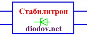
Conventional graphic designation of an element
Attention! A two-terminal network has conclusions: a cathode and an anode. If we consider the region of the pn junction, then the terminal connected to the p-region is the anode, and to the n-region is the cathode.
Semiconductor elements that are composed of two counter-directed zener diodes are called double-sided (two-node).
Double-sided zener diode
The classification of these two-terminal networks according to their functional purpose is as follows:
- parts for general use (discrete), power: 0-0.3; 0.3-5; 5-10 W and above;
- precision elements with a complex microcircuit in their structure (hidden structure);
- limiting zener diodes designed for interference suppressors.
The latter are designed for short-term transmission of pulsed current up to hundreds of amperes. Long-term operation with high currents causes overheating of the part and thermal breakdown.
Attention! A silicon diode (zener diode) connected to the circuit in the reverse direction has three types of breakdown: tunnel, avalanche, and caused by thermal instability. Their design implies the occurrence of the first two breakdowns before thermal destruction of the junction occurs.
Switching circuit and current-voltage characteristic (volt-ampere characteristic) Zener diode
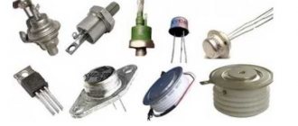
Types of diodes
A zener diode (Zener diode) is a type of semiconductor diode that operates at a reverse bias voltage in breakdown mode.
Until breakdown occurs, very insignificant leakage currents flow through the zener diode, and its resistance is quite high. At the moment of breakdown, the current through it increases sharply, and its differential resistance decreases to small values. Due to this, in the breakdown mode, the voltage on the zener diode is maintained with good accuracy in a wide range of reverse currents. The main separation of diodes occurs according to their type. There are three categories: material of manufacture, pn junction area and purpose.
Material
To produce diodes, one of four initial semiconductors is used:
- germanium - in low-power and precision circuits, has a higher transmission coefficient;
- silicon – inexpensive and durable, resistant to temperature, but less conductive;
- gallium arsenide – more expensive and more complex than silicon, high radiation resistance;
- indium phosphide - in LEDs and for operation at ultrahigh frequencies.
Each material in different systems has its own letter or number, which is indicated at the beginning.
Transition area
There are two options for the structural placement of the cathode and anode:
- Point diode. One of the electrodes in the form of a narrow needle is fused into the crystal, forming a pn boundary. It has a small area, which results in a high operating frequency. They are almost out of use due to low strength, vulnerability to overloads and low maximum current.
- Planar diode. The transition area is larger - the contact passes over the area of the semiconductor wafer connected to the crystal. They are distinguished by higher capacity, low noise level, and low voltage drop. An example is a Schottky diode.
In modern marking, separation practically does not occur - planar diodes are gradually replacing point diodes.
Subtype
The following designation depends on the purpose of the device. There is a classification of diodes used in different areas: tunnel, laser, varicaps, zener diodes. There is also a division within the subtype , based on technical parameters:
- operating frequency;
- recovery time;
- forward and reverse current;
- permissible values of reverse and forward voltage;
- temperature regime.
This results in a large number of possible combinations, hence the difficulty of creating a unified labeling system.
Marking of zener diodes
In order to find out the stabilization voltage of the Soviet zener diode, we need a reference book. For example, in the photo below there is a Soviet zener diode D814V:
We look for parameters for it in online directories on the Internet. As you can see, its stabilization voltage at room temperature is approximately 10 Volts.
Foreign zener diodes are marked more easily. If you look closely, you can see a simple inscription:
5V1 - this means the stabilization voltage of this zener diode is 5.1 Volts. Much easier, right?
The cathode of foreign zener diodes is marked mainly with a black stripe
Zener diode or Zener diode
The simplest voltage stabilizer in electronics is a zener diode . It is sometimes also called a Zener diode . In the diagrams, zener diodes are designated something like this:
The terminal with the “cap” is called the same as the diode - cathode , and the other terminal is anode .
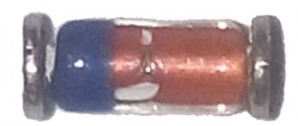
Zener diodes look the same as diodes. In the photo below, on the left is a popular type of modern zener diode, and on the right is one of the samples from the Soviet Union
If you take a closer look at the Soviet zener diode, you can see this schematic designation on it itself, indicating where its cathode is and where its anode is.
Main characteristics of a zener diode
To select a Zener diode for existing purposes, you need to know several important parameters. These characteristics will determine the suitability of the selected device for solving the assigned tasks.
Rated stabilization voltage
The first zener parameter that you need to pay attention to when choosing is the stabilization voltage, determined by the point at which the avalanche breakdown begins. This is where the choice of device to use in the circuit begins. For different instances of ordinary zener diodes, even of the same type, the voltage has a spread of around several percent; for precision ones, the difference is lower. If the nominal voltage is unknown, it can be determined by constructing a simple circuit. You should prepare:
- ballast resistor 1…3 kOhm;
- adjustable voltage source;
- voltmeter (you can use a tester).
It is necessary to increase the voltage of the power source from zero, monitoring the increase in voltage on the zener diode using a voltmeter. At some point it will stop, despite further increasing the input voltage. This is the actual stabilization voltage. If there is no regulated source, you can use a power supply with a constant output voltage obviously higher than Ustabilization. The measurement scheme and principle remain the same. But there is a risk of the semiconductor device failing due to exceeding the operating current.
Zener diodes are used to work with voltages from 2...3 V to 200 V. To generate a stable voltage below this range, other devices are used - stabistors, operating in the direct section of the current-voltage characteristic.
Operating current range
The current at which the zener diodes perform their function is limited above and below. From below it is limited by the beginning of the linear section of the reverse branch of the current-voltage characteristic. At lower currents, the characteristic does not provide a constant voltage mode.
The upper value is limited by the maximum dissipation power that the semiconductor device is capable of and depends on its design. Zener diodes in a metal case are designed for higher current, but do not forget about the use of radiators. Without them, the maximum permissible power dissipation will be significantly less.
Differential resistance
Another parameter that determines the operation of the zener diode is the differential resistance Rst. It is defined as the ratio of the voltage change ΔU to the current change ΔI that caused it. This quantity has the dimension of resistance and is measured in ohms. Graphically, this is the tangent of the angle of inclination of the working section of the characteristic. Obviously, the lower the resistance, the better the quality of stabilization. For an ideal (which does not exist in practice) zener diode Rst is equal to zero - any increase in current will not cause any change in voltage, and the section of the current-voltage characteristic will be parallel to the ordinate axis.
Selecting security chain parameters
8.1 Diode selection
Protective circuit diodes are selected based on the following conditions:
E < 0.7*Uadd. (5)
Considering that E = 220 V, we choose a diode of type D229B, which has Uadd = 400 V.
8.2 Selection of resistors
The resistor resistance values are determined using the curves in Fig. 4 and correspond to the intersection point of the curve Uм=f(Rp) with the straight line 0.7*Uadd.-E=0.7*400-220=60V, parallel to the Rр axis.
In the circuits presented in Fig. P-1b, P-2b, P-3b, the resistance of the protective circuit resistor is determined from the curves for relays RP-251, RPU-2 and are respectively equal to R = 2.4 kOhm, R5 = 4.2 kOhm , R7=4.2 kOhm.
The design case for the circuit in Fig. P-5c is the case of disconnection by contacts K3 of three parallel-connected relay windings K6, K7, K8 with the contacts K1 in the closed position. Moreover, if there is no protective circuit in the circuit in Fig. P-5c, then diodes VD1, VD2 are exposed to switching overvoltage. The resistance of the protective circuit resistor is defined as equivalent to three equal resistances connected in parallel, one of which (Rр) is determined from the curve in Fig. 4 for the RP-23 relay:
R2=Rр/3=2.2/3=0.773 kOhm
In the diagram shown in Fig. P-5c, it is worthy of attention to consider the possibility of relay K8 operating when contacts K2 are opened. The answer to this question in the case under consideration can be obtained by comparing the maximum value of the current passing through the winding of relay K8 in the transient mode with the minimum operating current of this relay. The current I passing in the winding of relay K8 when the contacts K2 is opened is the sum of current I1, which represents part of the sum of the currents in the windings of relays K4, K5 and current I2 - part of the sum of the currents in the windings of relays K6, K7. The maximum values of currents I1, I2, I are determined as follows:
Here: Ik4, Ik5, Ik6, Ik7 are the currents passing respectively in the relay windings K4, K5, K6, K7.
Where:
- 220 – power supply voltage (V);
- 9300, 9250 – direct current resistance, respectively, of the RP-23 relay winding and the RP-223 relay winding connected in series with the additional resistor (Ohm).
Minimum operating current of relay K8 (RP-23):
Thus, the amount of current passing in the winding of relay K8 when contacts K2 opens is insufficient to trigger the relay (If Im > Iav.k8, then relay K8 will operate when the condition tb > tav is met, where:
- tav – time during which Im > Iav.k8;
- tb – response time of relay K8.
Types of Zener diodes
There are three main types of zener diodes:
- Precision zener diodes - they are characterized by increased voltage stability. Example: 2S191 or KS211.
- Bilateral – limit and stabilize bipolar voltage. Example: 2С170А or 2С182А.
- High-speed zener diode - reduced barrier capacitance and low transient work - this makes it possible to work in the region of short-term voltage pulses. These are the following zener diodes: 2S175E; KS182E; 2S211E.
We recommend reading: How to measure resistance with a multimeter: instructions, photos, videos
Power distribution - these are high-power and low-power zener diodes.
SMD marking of electrical elements
The principle of marking is the encrypted transmission of information about the dimensions and electrical parameters of the chip. There is a conditional division according to the number of pins and the size of the element housing:
Interesting! Modern production covers almost all types of electronic elements produced in SMD format - resistors, diodes, inductive and capacitive components. An important component is the SMD zener diode, which power supplies, controllers and other critical devices cannot do without.
Chip capacitors
There are two main types of capacitors - electrolytic (the body is cylindrical) and ceramic or tantalum (the body is shaped like a parallelepiped). Electrolyte markings always contain capacitance and voltage values, but ceramic samples do not. The minus (cathode) of the electrolytes is indicated by a strip located on the upper side of the housing.
Marking of SMD resistors
The marking is represented by several characters - numbers and letters. The first two digits indicate the denomination, and the third (and fourth) indicate the order, or the number of zeros. For example, the number 322 means 3200 ohms or 3.2 kohms. Sometimes the R separator is used, acting as a comma. So, the designation 3R2 means 3.2 kOhm. Or 0R32 - 0.32 kOhm.
There are special resistors that act as fuses or jumpers. They have a zero resistance rating.
The dimensions of SMD devices are standardized and associated with markings. Thus, chips of diodes, resistors or capacitors of size 0805 have parameters of 0.6 × 0.8 × 0.23 inches (length-width-height).
SMD inductance
The shape and dimensions of the housings of the chokes and inductors have the same values as those of resistors or capacitors. The designation consists of 4 digits. The first two are the length, the others are the width of the chip, expressed in tenths of an inch. For example, the throttle marking 0805 means that its length is 0.08 and its width is 0.05 inches.
SMD diodes and transistors
Diode chips can be made in the form of a barrel or parallelepiped (briquette). All sizes fully correspond to the parameters of the resistors, which simplifies the development of printed circuit boards. Given the specific operation of diodes, for which polarity must be observed, there is a strip on or near the negative terminal. It designates the cathode, which helps avoid installation errors.
Interesting! The number of transistors produced by different manufacturers is very large, which causes considerable confusion in the labeling. It gets to the point where the same code refers to different types of transistors produced by different manufacturers. To clarify, you must have documentation for the board.
On the surface of the chip there can only be a code that does not provide complete information about the parameters of the part. Therefore, there are special information arrays - datasheets, which contain information about all the parameters and capabilities of the elements. If you need complete data on the properties that transistors have, the datasheet makes it possible to obtain detailed information.
Expert opinion
It-Technology, Electrical power and electronics specialist
Ask questions to the “Specialist for modernization of energy generation systems”
Table of designations and interpretation of LED color markings Example 2N2221A, 2N904 Color marking of semiconductor diodes according to the JEDEC system Stripe color Number 0 1 2 3 4 5 6 7 8 9 Letter - ABCDEFGH J. Ask, I'm in touch!
Types of 12 volt stabilizers
Depending on the design and method of maintaining a 12-volt voltage, there are two types of stabilizers:
- Pulse stabilizers, consisting of an integrator (battery, high-capacity electrolytic capacitor) and a switch (transistor). Maintaining the voltage in a given range of values occurs due to the cyclic process of accumulation and rapid release of charge by the integrator when the key is open. According to their design features and control method, such stabilizers are divided into key devices with a Schmitt trigger, equalizers with pulse width and pulse frequency modulation.
- Linear - voltage-stabilizing devices in which zener diodes or special microcircuits connected in series are used as a regulating device.
Pulse
Linear
The most common and popular among car enthusiasts are linear devices, characterized by ease of self-assembly, reliability and durability. The pulse type is used much less frequently due to the high cost of parts and the difficulties of independent production and repair.
Classic model
Classic stabilizers are a large class of devices assembled based on semiconductor parts such as bipolar transistors and zener diodes. Among them, the main function of maintaining the voltage at 12 V is performed by zener diodes - a type of diodes connected in reverse polarity (the plus of the power supply is connected to the cathode of such a semiconductor device, and the minus to the anode), operating in breakdown mode. The essence of how these semiconductor parts work is as follows:
- When the voltage of the power source connected to the zener diode is less than 12 V, it is in the closed position and does not participate in adjusting this characteristic of the electric current.
- When the threshold of 12 Volts is exceeded, the zener diode “opens” and maintains this value in the range specified by its characteristics.
If the voltage supplied to the zener diode exceeds that stated as the maximum by the manufacturer, the device very quickly fails due to the effect of thermal runaway.
In order for any zener diode model to serve as long as possible, it is recommended to specify the voltage range and current in which it should be operated according to its specifications. Depending on the connection, there are two versions of the classic stabilizer: linear - the adjusting elements are connected in series with the load; parallel – voltage stabilizing devices are located parallel to the powered devices.
Integral stabilizer
The devices are assembled using small-sized microcircuits capable of operating at an input voltage of up to 26-30 V, delivering a constant 12-volt current of up to 1 Ampere. A special feature of these radio components is the presence of 3 legs - “input”, “output” and “adjustment”. The latter is used to connect an adjustment resistor, which is used to adjust the microcircuit and prevent it from overloading.
More convenient and reliable equalizers assembled on the basis of stabilizing microcircuits are gradually replacing analogues assembled on discrete elements.
How to distinguish a stabilization diode from a conventional semiconductor
Very often people wonder how they can distinguish a zener diode from a standard semiconductor, because, as we found out earlier, both of these elements have almost identical symbols on the electrical circuit and can perform similar functions. The easiest way to distinguish a stabilization semiconductor from a regular one is to use a multimeter attachment circuit. With its help, you can not only distinguish both elements from each other, but also identify the stabilization voltage, which is characteristic of a given SMD (if it, of course, does not exceed 35V). The multimeter attachment circuit is a DC-DC converter, in which there is galvanic isolation between the input and output. This diagram looks like this:
Multimeter attachment circuit
In it, a generator with pulse-width modulation is implemented on a special microcircuit MC34063, and to create galvanic isolation between the measuring part of the circuit and the power source, the control voltage should be removed from the primary winding of the transformer. For this purpose there is a rectifier on VD2. In this case, the value for the output voltage or stabilization current is set by selecting resistor R3. A voltage of approximately 40V is released at capacitor C4. In this case, the tested SMD VDX and the stabilizer for current A2 will form a parametric stabilizer. The multimeter, which is connected to terminals X1 and X2, will measure the voltage at this zener diode. When connecting the cathode to the “-” and the anode to the “+” of the diode, as well as to the asymmetrical SMD of the multimeter, the latter will show a slight voltage. If you connect in reverse polarity (as in the diagram), then in a situation with a conventional semiconductor, the device will register a voltage of about 40V.
Note! For symmetrical SMD, the breakdown voltage will appear in the presence of any connection polarity.
Here the T1 transformer will be wound on a torus-shaped ferrite core with an outer diameter of 23 mm. Such winding 1 will contain 20 turns, and the second winding will contain 35 turns of PEV 0.43 wire. In this case, it is important to lay the turn to the turn when winding. It should be remembered that the primary winding goes on one part of the ring, and the second on the other. When setting up the device, connect a resistor instead of smd VDX. This resistor should have a value of 10 kOhm. And resistance R3 needs to be selected in order to achieve a voltage of 40V on capacitor C4. This is how you can find out whether you have a zener diode or a regular diode.
Features of using zener diodes
To use zener diodes, especially from Russian manufacturers, it is not advisable to operate outside the breakdown zone, which is a consequence of an increase in leakage current over time. For example, it is not recommended to apply a voltage different from the calculated value to a zener diode designed for U15 V; at least it is necessary to monitor the minimum stabilization current.
During an unsuccessful voltage dispersion, when it is selected to the limit value, the device may overheat and a breakdown mode may occur.
It is undesirable to connect zener diodes to the network as a fuse; the consequences for the zener diode will be disastrous; if the current value is exceeded, they will fail. For protection, it is best to use, in some cases, specialized zener diodes (suppressors) of the ZY5.6 brand. Installing a zener diode (Zener diode) in the low-voltage power supply circuit is extremely undesirable due to the fact that tunnel breakdown at U has a negative temperature coefficient.
Write comments, additions to the article, maybe I missed something. Take a look at the site map, I will be glad if you find anything else useful on my site.
Main conclusions
Knowledge of the markings of SMD diodes and other components will help when performing repair work, identifying analogues or options for replacing parts. To obtain detailed information about the parameters of elements, you must use the following sources:
- directory of SMD component codes;
- datasheet (mainly for transistors);
- deciphering the code for resistors or chokes.
The number of SMD diodes and other parts is large. Many manufacturers develop their own marking system, which is in no way correlated with other designations, which introduces significant confusion into the process of identifying and replacing problematic elements. Therefore, it is important to have reference books and complete blocks of information on the parameters of diodes or other parts from different companies on hand.
How to check zener diode
How to check the zener diode? Yes, just like a diode! You can see how to check the diode in this article. Let's check our zener diode. We put the multimeter on the continuity test and attach the red probe to the anode, and the black probe to the cathode. The multimeter should show the voltage drop of the forward PN junction.
We swap the probes and see one. This means that our zener diode is in full combat readiness.
Well, it's time for experiments. In the circuits, a zener diode is connected in series with a resistor:
where Uin – input voltage, Uout.st. – output stabilized voltage
If we look closely at the diagram, we get nothing more than a voltage divider. Everything here is elementary and simple:
Uin=Uout.stab +Uresistor
Or in words: the input voltage is equal to the sum of the voltages on the zener diode and the resistor.
This circuit is called a parametric stabilizer on one zener diode. The calculation of this stabilizer is beyond the scope of this article, but for those interested, Google it.
So, let's put together the circuit. We took a resistor with a nominal value of 1.5 Kilohms and a zener diode with a stabilization voltage of 5.1 Volts. On the left we connect the Power Supply, and on the right we measure the resulting voltage with a multimeter:
Now we carefully monitor the readings of the multimeter and power supply:
So, while everything is clear, let’s add more tension... Oops! Our input voltage is 5.5 Volts, and our output voltage is 5.13 Volts! Since the stabilization voltage of the zener diode is 5.1 Volts, as we can see, it stabilizes perfectly.
Let's add some more volts. The input voltage is 9 Volts, and the zener diode is 5.17 Volts! Amazing!
We also add... The input voltage is 20 Volts, and the output, as if nothing had happened, is 5.2 Volts! 0.1 Volt is a very small error, it can even be neglected in some cases.
Basic circuit of a parallel stabilizer
The simplest parallel stabilizer consists of a ballast resistor connected in series between the power source and the load, and a zener diode that shunts the load to a common wire (“to ground”). It can be considered as a voltage divider, in which a zener diode is used as the lower arm. The difference between the supply voltage and the breakdown voltage of the zener diode drops across the ballast resistor, and the supply current flowing through it branches into the load current and the zener diode current. Stabilizers of this kind are called parametric: they stabilize the voltage due to the nonlinearity of the current-voltage characteristic of the zener diode, and do not use feedback circuits.
We recommend reading: The principle of operation of a transistor multivibrator
The calculation of a parametric stabilizer on semiconductor zener diodes is similar to the calculation of a stabilizer on gas-filled devices, with one significant difference: gas-filled zener diodes are characterized by threshold voltage hysteresis. When there is a capacitive load, the gas-filled zener diode is self-excited, so the designs of such stabilizers usually do not contain capacitive filters, and the designer does not need to take into account transient processes in these filters. In stabilizers based on semiconductor zener diodes, there is no hysteresis; filter capacitors are connected directly to the terminals of the zener diode and the load - as a result, the designer must take into account the surge current of the charge (discharge) of these capacitors when turning the power on (off). The worst cases in which the stabilizer elements are likely to fail or stabilization to fail are:
- Supplying the maximum possible supply voltage to the input of the stabilizer in the event of a short circuit of the stabilizer output to the common wire - for example, while charging a discharged capacitor connected directly to the output of the stabilizer, or in the event of a catastrophic failure of the zener diode. The permissible power dissipation of the ballast resistor must be sufficient to withstand such a short circuit. Otherwise, the ballast resistor is likely to be destroyed.
- Supplying the maximum possible supply voltage to the stabilizer input when the load is disconnected from the stabilizer output. The permissible current of the zener diode must exceed the calculated current through the ballast resistor, determined by Ohm's law. Otherwise, when the zener diode crystal is heated above +175 °C, the zener diode is destroyed. Compliance with the safety data sheet is just as important for zener diodes as for transistors.
- The load selects the maximum possible current when the minimum possible supply voltage is supplied to the stabilizer input. The resistance of the ballast resistor must be small enough so that, even under these conditions, the current through the resistor exceeds the load current by an amount equal to the minimum permissible current of the zener diode. Otherwise, the zener diode current is interrupted and stabilization stops.
In practice, it often turns out that it is impossible to meet all three conditions, both for reasons of the cost of components and because of the limited range of operating currents of the zener diode. First of all, you can sacrifice the condition of short circuit protection, entrusting it to fuses or thyristor protection circuits, or rely on the internal resistance of the power supply, which will not allow it to produce both the maximum voltage and maximum current at the same time.
Series and parallel connection
In the documentation for foreign-made zener diodes, the possibility of their serial or parallel connection is usually not considered. In the documentation for Soviet zener diodes there are two formulations:
- for low and medium power devices, “serial or parallel connection of any number of zener diodes” [of the same series] is allowed;
- for medium and high power devices, “a series connection of any number of zener diodes [of the same series] is allowed.” Parallel connection is permitted provided that the total power dissipation on all parallel-connected zener diodes does not exceed the maximum permissible power for one zener diode."
Series connection of zener diodes of different series is possible provided that the operating currents of the series chain fall within the certified stabilization current ranges of each series used. There is no need to shunt zener diodes with high-resistance equalizing resistors, as is done in rectifier columns. “Any number” of zener diodes connected in series is possible, but in practice is limited by technical conditions for the electrical safety of high-voltage devices. Subject to these conditions, when selecting zener diodes according to TKN and their thermostatting, it is possible to construct precision high-voltage voltage standards. For example, in the 1990s, the zener diode standard of 1 million V, built by Russia at the request of the Canadian energy institute IREQ, had the best stability indicators in the world. The main error of this installation did not exceed 20 ppm, and the temperature instability did not exceed 2.5 ppm over the entire operating temperature range.
Composite Zener diode
If the circuit requires removing higher currents and powers from the zener diode than is permissible according to the technical conditions, then a DC buffer amplifier is connected between the zener diode and the load. In the “composite zener diode” circuit, the collector junction of the single current-amplifying transistor is connected in parallel with the zener diode, and the emitter junction is in series with the zener diode. The resistance that sets the bias of the transistor is selected so that the transistor smoothly turns on at a zener diode current approximately equal to its rated stabilization current. For example, with Ist.nom.=5 mA and Ube.min. =500 mV resistance R=500 mV/5 mA=100 Ohm, and the voltage on the “composite zener diode” is equal to the sum of Ust.nom. and Ube.min.. At high currents, the transistor opens and shunts the zener diode, and the zener diode current increases slightly - by an amount equal to the base current of the transistor, therefore, to a first approximation, the differential resistance of the circuit decreases by a factor (is the current gain of the transistor). The TKN of the circuit is equal to the algebraic sum of the TKN of the zener diode at Ist.nom. and TKN of a forward biased diode (approximately -2 mV/°C), and its area of safe operation in practice is limited by the OBR of the transistor used.
Connection methods - serial and parallel
For imported parts in the accompanying documents, situations in which a serial or parallel connection is possible are not regulated. In the documentation for domestic reference diodes you can find two instructions:
- In devices of small and medium power, any number of single-series zener diodes can be connected in series or in parallel.
- In devices of medium and high power, any number of stabilizing diodes of a single series can be connected in series. For a parallel connection, calculations must be made. The total power dissipation of all parallel-connected zener diodes should not be higher than that of one part.
It is possible to connect reference diodes of different series in series if the operating currents of the created circuit do not exceed the rated stabilization currents for each series installed in the circuit.
In practice, to multiply the stabilization voltage, a series connection of two or three zener diodes is most often used. This measure is resorted to if it was not possible to obtain a part for the required voltage or it is necessary to create a high-voltage zener diode. When connected in series, the voltage of the individual elements is summed. This type of connection is mainly used in the assembly of high-voltage stabilizers.
Parallel connection of parts serves to increase current and power. However, in practice, this type of connection is rarely used, since different instances of reference diodes, even of the same type, do not have exactly the same stabilization voltages. Therefore, with a parallel connection, a discharge will occur only in the part with the lowest stabilization voltage, and breakdown will not occur in the rest. If a breakdown occurs, then some zener diodes in such a circuit will operate with underload, and others with overload.
To stabilize the alternating voltage, the zener diodes are connected in series and back-to-back. In the first half-cycle of an alternating current sinusoid, one element operates as a regular diode, and the second performs the functions of a zener diode. In the second half-cycle, the elements change functions. The output voltage shape is different from the input voltage. Its configuration resembles a trapezoid. This is due to the fact that a voltage exceeding the stabilization voltage will be cut off and the tops of the sine wave will be cut off. Series and counter connection of zener diodes can be used in a temperature-stabilized zener diode.
Basic parameters of zener diodes
In order to select the right zener diode, you need to understand the markings of semiconductor devices. Previously, all types of diodes, including zener diodes, were designated by the letter “D” and a number indicating what kind of device it was. Here is an example of the very popular D814 zener diode (A, B, C, D). The letter showed the stabilization voltage.
| D814B | 2С147А |
|
|
Nearby are the passport data of a modern zener diode (2C147A), which was used in stabilizers to power circuits based on the popular series of K155 and K133 microcircuits made using TTL technology and having a supply voltage of 5V.
To understand the markings and basic parameters of modern domestic semiconductor devices, you need to know a little about the symbols. They look like this: number 1 or letter G - germanium, number 2 or letter K - silicon, number 3 or letter A - gallium arsenide. This is the first sign. D – diode, T – transistor, S – zener diode, L – LED. This is the second sign. The third character is a group of numbers indicating the scope of application of the device. Hence: GT 313 (1T 313) - high-frequency germanium transistor, 2S147 - silicon zener diode with a nominal stabilization voltage of 4.7 volts, AL307 - gallium arsenide LED.
Here is a diagram of a simple but reliable voltage stabilizer.
Recommended reading: Stepper motor control
A voltage of 12–15 volts is supplied between the collector of the powerful transistor and the housing from the rectifier. We remove 9V stabilized voltage from the emitter of the transistor, since we use the reliable D814B element as the zener diode VD1 (see table). Resistor R1 is 1 kOhm, transistor KT819 provides current up to 10 amperes.
The transistor must be placed on the heat sink. The only drawback of this circuit is the inability to adjust the output voltage. In more complex circuits, of course, there is a tuning resistor. All laboratory and home amateur radio power sources have the ability to adjust the output voltage from 0 to 20 - 25 volts.
Details about the color coding of the stabilizing diode
Any diode (zener diode, etc.) contains a special marking on its case, which reflects what material was used to manufacture each specific semiconductor. Such marking may look like this:
- letter or number;
- letter.
In addition, the marking reflects the electrical properties and purpose of the device. Usually a number is responsible for this. The letter, in turn, reflects the corresponding type of device. In addition, the marking contains the date of manufacture and the symbol of the product. Integral type SMDs often contain full markings. In such a situation, there is a conditional code on the product body that indicates the type of microcircuit. An example of decoding the code markings for microcircuits applied to the housing is shown in the figure:
Example of microcircuit marking
In addition, there is also color coding. It exists in several versions, but the most commonly used is the Japanese marking (JIS-C-7012). The color coding is shown in the following table.
The principle of operation of a zener diode
First of all, we should not forget that the zener diode only works in DC circuits. The voltage is applied to it in reverse polarity, that is, a minus “-” will be applied to the anode of the zener diode. With this connection, reverse current flows through it (I return) from the rectifier. The voltage from the rectifier output can change, the reverse current will also change, but the voltage at the zener diode and at the load will remain unchanged, that is, stable. The following figure shows the current-voltage characteristic of a zener diode.
The zener diode operates on the reverse branch of the current-voltage characteristic (volt-ampere characteristic), as shown in the figure. Its main parameters include U st. (stabilization voltage) and I st. (stabilization current). These data are indicated in the passport for a specific type of zener diode. Moreover, the value of the maximum and minimum current is taken into account only when calculating stabilizers with a predicted large voltage change.
How to choose a transistor for a stabilizer?
The main parameters for a transistor in a voltage stabilizer are: maximum collector current, maximum collector-emitter voltage and maximum power. All these parameters are always available in reference books. 1. When choosing a transistor, it is necessary to take into account that the passport (according to the reference book) maximum collector current must be no less than one and a half times the maximum load current that you want to receive at the output of the stabilizer. This is done in order to provide a margin of load current during random short-term load surges (for example, a short circuit). It should be taken into account that the greater this difference, the less massive the cooling radiator the transistor requires.
Zener diode connection circuits
The main circuit for connecting a zener diode is in series with a resistor, which sets the current through the semiconductor device and takes on the excess voltage. Two elements make up a common divisor. When the input voltage changes, the drop across the zener diode remains constant, but across the resistor changes.
Such a circuit can be used independently and is called a parametric stabilizer. It keeps the load voltage constant despite fluctuations in input voltage or current consumption (within certain limits). A similar block is also used as an auxiliary circuit where a reference voltage source is needed.
Such a connection is also used to protect sensitive equipment (sensors, etc.) from abnormal occurrence of high voltage in the power or measurement line (constant or random pulses). Everything above the stabilization voltage of the semiconductor device is “cut off”. This scheme is called the “Zener barrier”.
Previously, the property of a zener diode to “cut off” voltage peaks was widely used in pulse shaper circuits. In alternating current circuits, two-anode devices were used.
But with the development of transistor technology and the advent of integrated circuits, this principle began to be rarely used.
If you don’t have a zener diode for the required voltage at hand, it can be made up of two. The total stabilization voltage will be equal to the sum of the two voltages.
Important! You cannot connect zener diodes in parallel to increase the operating current! A scatter in the current-voltage characteristics will lead to one zener diode entering the thermal breakdown zone, and then the second will fail due to excess load current.
Although technical documentation from the times of the USSR allows the inclusion of parallel zeners in parallel, but with the caveat that the devices must be of the same type and the total actual power dissipation during operation should not exceed that permissible for a single zener diode. That is, an increase in operating current under this condition cannot be achieved.
To increase the permissible load current, another circuit is used. The parametric stabilizer is supplemented with a transistor, and an emitter follower is obtained with a load in the emitter circuit and a stable voltage at the base of the transistor.
In this case, the output voltage of the stabilizer will be less than Ustabilization by the amount of the voltage drop across the emitter junction - for a silicon transistor, about 0.6 V. To compensate for this decrease, you can connect a diode in series with the zener diode in the forward direction.
In this way (by turning on one or more diodes) you can adjust the output voltage of the stabilizer upward within small limits. If you need to radically increase Uout, it is better to connect another zener diode in series.
The scope of application of the zener diode in electronic circuits is extensive. With a conscious approach to selection, this semiconductor device will help solve many problems assigned to the developer.
Composite Zener diodes
Composite zener diode is a device used in situations where currents and power greater than those allowed by technical conditions are required. In this case, a DC buffer amplifier is connected between the stabilizing diode and the load. In the circuit, the collector junction of the transistor is connected in parallel with the stabilizing diode, and the emitter junction is connected in series.
The circuit of a conventional composite zener diode is not intended for direct current use. But adding a diode bridge turns the compound zener diode into a dual-acting system that can operate with both forward and reverse current. Such zener diodes are also called double or two-anode. Zener diodes that can operate with voltage of only one polarity are called asymmetrical. And composite zener diodes, capable of operating in any direction of current, are called symmetrical.
How to make a 12V stabilizer
Simple, but at the same time quite effective, reliable and durable stabilizing devices can be made independently, using simple zener diodes and special small microcircuits such as LM317, LD1084, L7812, KREN (KR142EN8B).
Stabilizer on LM317
The assembly process of such a voltage-stabilizing device consists of the following steps:
- A 130-ohm resistance is soldered to the middle output contact of the microcircuit.
- A conductor is soldered to the input right contact, supplying an unstabilized voltage from the power source.
- The left adjustment contact is soldered to the second leg of the resistor installed at the output of the microcircuit.
The soldering process of such a stabilizer takes no more than 10 minutes and, taking into account the inexpensive microcircuit, does not require large investments. Using a similar device, LED lights and strips are powered.
Chip LD1084
The assembly of a device for stabilizing the voltage of an automobile on-board network using the LD1084 microcircuit is carried out as follows:
- A conductor with positive voltage from the diode bridge is soldered to the input contact of the microcircuit.
- The emitter of a bipolar transistor is soldered to the adjustment contact, the base of which, through two resistors with a nominal value of 1 kOhm, supplies the current of the low and high beam headlights.
- Two resistors are soldered to the output contact (one is a regular 120 Ohm, and the second is a trimmer, 4.7 kOhm) and a 10 µF electrolytic capacitor
To smooth out the current ripple, another electrolytic capacitor with a capacity of 10 μF is installed after the diode bridge.
Adjustable Zener Diodes
When manufacturing stabilized power supplies, the necessary zener diode may be missing. In this case, an adjustable zener diode circuit is assembled.
The required voltage of the stabilizing diode is selected using resistor R1. To configure the circuit, a variable resistor with a nominal value of 10 kOhm is connected in place of resistor R1. After obtaining the required voltage value, determine the resulting resistance and install a resistor of the required value in a permanent place. For this circuit, you can use transistors KT342A, KT3102A.
Color coding of diodes in SOD-80 packages
The SOD-80 body, also known as MELF, is a small glass cylinder with metal leads.
Marking 2Y4 to 75Y (E24 series) BZV49 1W silicon zener diode (2.4 - 75V) Marking C2V4 to C75 (E24 series) BZV55 500mW silicon zener diode (2.4 - 75V)
Some SMD diodes in MiniMELF (SOD80 / DO213AA / LL34) or MELF (DO213AB / LL41) cylindrical packages are often marked with colored stripes (the first stripe closest to the edge is located at the cathode) in accordance with the table on the left.
Useful tips Connection diagrams Principles of operation of devices Main concepts Meters from Energomer Precautions Incandescent lamps Video instructions for the master Testing with a multimeter
Designations for the operation of an electrical circuit element
Schematic designation of a zener diode
Since the zener diode is a special diode, its designation is no different from them. Schematically, smd is designated as follows:
A zener diode, like a diode, has a cathode and anode part. Because of this, there is direct and reverse inclusion of this element.
At first glance, the inclusion of such a diode is incorrect, because it should be connected “the other way around”. In a situation where reverse voltage is applied to the SMD, the phenomenon of “breakdown” is observed. As a result, the voltage between its terminals remains unchanged. Therefore, it must be connected in series to a resistor in order to limit the current passing through it, which will ensure that the “excess” voltage from the rectifier drops.
Note! Each diode designed to stabilize voltage has its own “breakdown” (stabilization) voltage and also has its own operating current.
Due to the fact that each zener diode has such characteristics, it is possible to calculate the value of the resistor that will be connected in series with it. For imported zener diodes, their stabilization voltage is presented in the form of markings on the body (glass or not). The designation of such an smd diode always begins with BZY... or BZX..., and their breakdown (stabilization) voltage is marked V. For example, the designation 3V9 stands for 3.9 volts.
Note! The minimum voltage for stabilization of such elements is 2 V.
Marking of SMD diodes, reference codes
Existing SMD diodes or other types of parts may be called chips, or SMD components. In Russian schematics and industry they are often called TMP - surface mounting technology. The number of parts is very large, so the designations are collected in electronic databases and can be saved to a computer for quickly identifying a diode or other component. The volumes of the databases are different, but they all include several thousand designations.
It is useful for any practitioner to have such a reference book so as not to waste time recognizing markings, searching for analogues or other use cases. Sometimes it becomes possible to replace conventional diodes or other parts with chips, which gives a considerable gain:
- size decreases;
- parasitic effects manifested in capacitance and inductance are reduced;
- work with low-level signals is improved.
At first glance, it is not easy to understand the variety of chips, however, the compilers of reference books understand this and combine all the data into groups. Diodes, capacitors, resistors and other types are considered separately. This makes it somewhat easier to navigate through huge amounts of data.