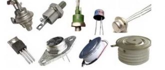
Device
Semiconductor zener diodes have replaced the obsolete glow discharge zener diodes - ion gas-discharge electric vacuum devices. For the manufacture of zener diodes, silicon or germanium crystals (tablets) with n-type conductivity are used, into which impurities are added by an alloy or diffuse alloy method. To obtain an electron-hole pn junction, acceptor impurities, mainly aluminum, are used. The crystals are enclosed in housings made of polymer materials, metal or glass.
Silicon alloy zener diodes D815 (A-I) are produced in a sealed metal case, which is the positive electrode. Such elements have a wide operating temperature range – from -60°C to +100°C. Silicon alloy two-anode stabilizing diodes KS175A, KS182A, KS191A, KS210B, KS213B are produced in a plastic case. Silicon alloy temperature-compensated parts KS211 (B-D), used as reference voltage sources, have a plastic housing.
SMD zener diodes, that is, miniature components intended for surface mounting, are manufactured mainly in glass and plastic cases. Such elements can be produced with two or three terminals. In the latter case, the third pin is a “dummy”, does not carry any semantic load and is intended only for reliable fixation of the part on the printed circuit board.
Marking of SMD zener diodes
The most widely used reference diodes are in a glass case and in a plastic case with three terminals. The SMD marking of a zener diode in a glass case consists of a colored ring, the color of which indicates the parameters of this semiconductor device.
If you come across an SMD zener diode with three terminals, then you should know that one terminal is a “dummy”, that is, it is not used and is used only for securely fixing the element on the printed circuit board after soldering. The anode and cathode of such an instance are most easily determined using a multimeter.
Operating principle
The zener diode was discovered by the American physicist Clarence Melvin Zener, after whom it was named. Electrical breakdown of a pn junction can be caused by a tunnel breakdown (in this case, the breakdown is called Zener breakdown), avalanche breakdown, breakdown as a result of thermal instability, which occurs due to destructive self-heating by leakage currents.
And engineers design these elements in such a way that the occurrence of tunneling and/or avalanche breakdown occurs long before they are likely to experience thermal breakdown.
The magnitude of the breakdown voltage depends on the concentration of impurities and the method of doping of the pn junction. The greater the concentration of impurities and the higher their gradient in the junction, the lower the reverse voltage at which a breakdown occurs.
- A tunnel (Zener) breakdown
appears in a semiconductor in cases where the electric field strength in the pn zone is 106 V/cm. Such high voltage can only occur in highly doped diodes. At breakdown voltages in the range of 4.5...6.7 V, the tunnel and avalanche effects coexist, but at a breakdown voltage less than 4.5 V, only the tunnel effect remains. - In zener diodes with low doping levels or smaller gradients of dopant additives there is only an avalanche breakdown mechanism
, which appears at a breakdown voltage of approximately 4.5 V. And at voltages above 7.2 V, only the avalanche effect remains, and the tunnel effect disappears completely.
As mentioned earlier, when connected directly, the zener diode behaves in the same way as a regular diode when connected directly - it passes current. The differences between them arise when connecting in reverse.
A conventional diode, when connected in reverse, blocks the current, and the zener diode, when the reverse voltage reaches a value called the stabilization voltage, begins to pass current in the opposite direction. This is explained by the fact that when a voltage exceeding U nom is applied to the zener diode. device, a process called breakdown occurs in the semiconductor. The breakdown can be tunnel, avalanche, or thermal. As a result of the breakdown, the current flowing through the zener diode increases to a maximum value limited by the resistor. After reaching the breakdown voltage, the current remains approximately constant over a wide range of reverse voltages. The point at which voltage triggers current can be very precisely set during the manufacturing process by doping. Therefore, each element is assigned a certain breakdown (stabilization) voltage.
The zener diode is used only in “reverse bias” mode, that is, its anode is connected to the “-” power supply. The ability of a zener diode to trigger reverse current when the breakdown voltage is reached is used to regulate and stabilize the voltage when the supply voltage or connected load changes. The use of a zener diode makes it possible to provide a constant output voltage for the connected consumer when the power supply voltage drops or the consumer current changes.
Features of using zener diodes
To use zener diodes, especially from Russian manufacturers, it is not advisable to operate outside the breakdown zone, which is a consequence of an increase in leakage current over time. For example, it is not recommended to apply a voltage different from the calculated value to a zener diode designed for U15 V; at least it is necessary to monitor the minimum stabilization current.
During an unsuccessful voltage dispersion, when it is selected to the limit value, the device may overheat and a breakdown mode may occur.
It is undesirable to connect zener diodes to the network as a fuse; the consequences for the zener diode will be disastrous; if the current value is exceeded, they will fail. For protection, it is best to use, in some cases, specialized zener diodes (suppressors) of the ZY5.6 brand. Installing a zener diode (Zener diode) in the low-voltage power supply circuit is extremely undesirable due to the fact that tunnel breakdown at U has a negative temperature coefficient.
Write comments, additions to the article, maybe I missed something. Take a look at the site map, I will be glad if you find anything else useful on my site.
Volt-ampere characteristics
The current-voltage characteristic of a zener diode, like a conventional diode, has two branches - forward and reverse. The forward branch is the operating mode for a traditional diode, and the reverse branch characterizes the operation of the zener diode. A zener diode is called a reference diode, and a voltage source that contains a zener diode in its circuit is called a reference diode.
On the working reverse branch of the reference diode, three main values of the reverse current are distinguished:
- Minimum
. When the current is less than the minimum value, the zener diode remains closed. - Optimal
. When the current changes within a wide range between points 1 and 3, the voltage value changes insignificantly. - Maximum
. When applying current above the maximum value, the reference diode will overheat and fail. The maximum current value is limited by the maximum permissible power dissipation, which is highly dependent on external temperature conditions.
The principle of operation of a zener diode
Let's consider the principle of operation of a zener diode using the example of its connection circuit and current-voltage characteristic. To perform its main function, the zener diode VD is connected in series with a resistor Rb and together they are connected to a source of unstabilized input voltage Uin. The already stabilized output voltage Uout is removed only from pins 2, 3 VD. Therefore, the load Rн is connected to the corresponding points 2 and 3. As can be seen from the diagram, VD and Rb form a voltage divider. Only the resistance of the zener diode does not have a constant value and is called dynamic, since it depends on the amount of electric current flowing through the semiconductor device.
The voltage Uin supplied to the zener diode from the resistors must be at least a couple of volts higher than the output voltage Uout, otherwise the semiconductor device VD will not open and will not be able to perform its main function.
Let's say that at some arbitrary point in time at outputs 1 and 3 the value of Uin began to increase. The following processes will begin to occur in the circuit. As the voltage increases, according to Ohm's law, the current will begin to increase, let's call it the input current Iin. As the current increases, the voltage drop across the resistor Rb will increase, and at VD it will remain unchanged (this will be explained further in the characteristic), therefore Uout will remain at the same level. Consequently, the increase in input voltage will drop or be extinguished by resistor Rb. Therefore, Rb is called damping or ballast.
Now, let’s say the load has changed, for example, the resistance Rн has decreased, and the current In will increase accordingly. In this case, the current flowing through the zener diode Ist will decrease, and Iin will remain virtually unchanged.
Areas of use
The main area of application of these elements is stabilization of direct voltage in low-power power supplies or in individual units with a power of no more than tens of watts. With the help of reference diodes, they ensure the normal operating mode of transistors, microcircuits, and microcontrollers.
In simple design stabilizers, the zener diode is both a reference voltage source and a regulator. In more complex designs, the zener diode serves only as a source of reference voltage, and an external power transistor is used for power regulation.
Temperature-compensated zener diodes and parts with a hidden structure are in demand as discrete and integrated reference voltage sources. To protect electrical equipment from overvoltages, pulse avalanche zener diodes have been developed. To protect the inputs of electrical devices and the gates of field-effect transistors, ordinary low-power zener diodes are installed in the circuit. Insulated gate field-effect transistors (IGFETs) are manufactured with a single chip on which are located: a protective zener diode and a power transistor.
Main characteristics
The passport of the stabilizing diode indicates the following parameters:
- Rated stabilization voltage Ust
. This setting is selected by the device manufacturer. - Operating current range
. Minimum current – the current value at which the stabilization process begins. Maximum current is the value above which the device is destroyed. - Maximum power dissipation
. In low-power elements this is the nameplate value. In the passports of high-power zener diodes, to calculate the cooling conditions, the manufacturer indicates: the maximum permissible temperature of the semiconductor and the coefficient of thermal resistance of the housing.
In addition to the parameters indicated in the passport, zener diodes are characterized by other quantities, including:
- Differential resistance
. This property determines the instability of the device in terms of supply voltage and load current. The first drawback is eliminated by powering the stabilizing diode from a direct current source, and the second by connecting a DC buffer amplifier with an emitter follower between the zener diode and the load. - Temperature coefficient of voltage
. In accordance with the standard, this value is equal to the ratio of the relative change in stabilization voltage to the absolute change in outside temperature. In non-heat-stabilized zener diodes, when heated from +25°C to +125°C, the stabilization voltage shifts by 5-10% from the original value. - Drift and noise
. These characteristics are not defined for conventional zener diodes. For precision devices they are very important properties. In conventional (non-precision) zener diodes, noise is created by: a large number of foreign impurities and crystal lattice defects in the region of the pn junction. Methods for reducing noise (if necessary): protective passivation with oxide or glass (impurities are directed deep into the crystal) or by moving the pn junction itself deep into the crystal. The second method is more radical. It is in demand in low noise diodes with a hidden structure.
Basic parameters of zener diodes
In order to select the right zener diode, you need to understand the markings of semiconductor devices. Previously, all types of diodes, including zener diodes, were designated by the letter “D” and a number indicating what kind of device it was. Here is an example of the very popular D814 zener diode (A, B, C, D). The letter showed the stabilization voltage.
| D814B | 2С147А |
|
|
Nearby are the passport data of a modern zener diode (2C147A), which was used in stabilizers to power circuits based on the popular series of K155 and K133 microcircuits made using TTL technology and having a supply voltage of 5V.
To understand the markings and basic parameters of modern domestic semiconductor devices, you need to know a little about the symbols. They look like this: number 1 or letter G - germanium, number 2 or letter K - silicon, number 3 or letter A - gallium arsenide. This is the first sign. D – diode, T – transistor, S – zener diode, L – LED. This is the second sign. The third character is a group of numbers indicating the scope of application of the device. Hence: GT 313 (1T 313) - high-frequency germanium transistor, 2S147 - silicon zener diode with a nominal stabilization voltage of 4.7 volts, AL307 - gallium arsenide LED.
Here is a diagram of a simple but reliable voltage stabilizer.
Recommended reading: Stepper motor control
A voltage of 12–15 volts is supplied between the collector of the powerful transistor and the housing from the rectifier. We remove 9V stabilized voltage from the emitter of the transistor, since we use the reliable D814B element as the zener diode VD1 (see table). Resistor R1 is 1 kOhm, transistor KT819 provides current up to 10 amperes.
The transistor must be placed on the heat sink. The only drawback of this circuit is the inability to adjust the output voltage. In more complex circuits, of course, there is a tuning resistor. All laboratory and home amateur radio power sources have the ability to adjust the output voltage from 0 to 20 - 25 volts.
Connection methods - serial and parallel
For imported parts in the accompanying documents, situations in which a serial or parallel connection is possible are not regulated. In the documentation for domestic reference diodes you can find two instructions:
- In devices of small and medium power, any number of single-series zener diodes can be connected in series or in parallel.
- In devices of medium and high power, any number of stabilizing diodes of a single series can be connected in series. For a parallel connection, calculations must be made. The total power dissipation of all parallel-connected zener diodes should not be higher than that of one part.
It is possible to connect reference diodes of different series in series if the operating currents of the created circuit do not exceed the rated stabilization currents for each series installed in the circuit.
In practice, to multiply the stabilization voltage, a series connection of two or three zener diodes is most often used. This measure is resorted to if it was not possible to obtain a part for the required voltage or it is necessary to create a high-voltage zener diode. When connected in series, the voltage of the individual elements is summed. This type of connection is mainly used in the assembly of high-voltage stabilizers.
Parallel connection of parts serves to increase current and power. However, in practice, this type of connection is rarely used, since different instances of reference diodes, even of the same type, do not have exactly the same stabilization voltages. Therefore, with a parallel connection, a discharge will occur only in the part with the lowest stabilization voltage, and breakdown will not occur in the rest. If a breakdown occurs, then some zener diodes in such a circuit will operate with underload, and others with overload.
To stabilize the alternating voltage, the zener diodes are connected in series and back-to-back. In the first half-cycle of an alternating current sinusoid, one element operates as a regular diode, and the second performs the functions of a zener diode. In the second half-cycle, the elements change functions. The output voltage shape is different from the input voltage. Its configuration resembles a trapezoid. This is due to the fact that a voltage exceeding the stabilization voltage will be cut off and the tops of the sine wave will be cut off. Series and counter connection of zener diodes can be used in a temperature-stabilized zener diode.
Composite Zener diodes
Composite zener diode is a device used in situations where currents and power greater than those allowed by technical conditions are required. In this case, a DC buffer amplifier is connected between the stabilizing diode and the load. In the circuit, the collector junction of the transistor is connected in parallel with the stabilizing diode, and the emitter junction is connected in series.
The circuit of a conventional composite zener diode is not intended for direct current use. But adding a diode bridge turns the compound zener diode into a dual-acting system that can operate with both forward and reverse current. Such zener diodes are also called double or two-anode. Zener diodes that can operate with voltage of only one polarity are called asymmetrical. And composite zener diodes, capable of operating in any direction of current, are called symmetrical.
Operating principle of stabilization diodes
Despite the fact that the SMD is similar to a diode, it is essentially a different element of the electrical circuit. Of course, it can serve as a rectifier, but is usually used to stabilize the voltage. This element is capable of maintaining a constant voltage in a DC circuit. This principle of operation is used in power supply of various radio equipment.
Zener diode and diode
Externally, SMD is very similar to a standard semiconductor. The similarity remains in the design features. But when designating such a radio element, unlike a diode, the letter G is placed on the diagram. If you do not delve into mathematical calculations and physical phenomena, then the operating principle of smd will be quite clear.
Passing through this element, a small voltage in the circuit provokes a strong current. As the reverse voltage increases, the current also increases, only in this case its growth will be observed weakly. When you reach the mark, it can be anything. It all depends on the type of device. When the mark is reached, a “breakdown” occurs. After the “breakdown” has occurred, a large reverse current begins to flow through the smd. It is at this moment that the operation of this element begins until its permissible limit is exceeded.
Types of Zener diodes
On the modern electronics market there is a wide range of zener diodes adapted to specific application conditions.
Precision
These devices provide high output voltage stability. They are subject to additional requirements regarding the temporary instability of voltage and temperature coefficient of voltage. Precision devices include:
- Temperature compensated
. The temperature-compensated zener diode circuit includes a series-connected zener diode with a nominal voltage of 5.6 V (with a positive temperature coefficient) and a directly illuminated diode (with a negative coefficient). When these elements are connected in series, mutual compensation of temperature coefficients occurs. Instead of a diode, a second zener diode can be used in the circuit, connected in series and counter. - With hidden structure
. The breakdown current in a conventional zener diode is concentrated in the near-surface silicon layer, where the maximum amount of foreign impurities and crystal lattice defects is located. These design imperfections cause noise and unstable operation. In parts with a hidden structure, the breakdown current is “driven” inside the crystal by forming a deep island of p-type conductivity.
Fast acting
They are characterized by: a low value of the barrier capacitance, only tens of picofarads, and a short period of the transient process (nanoseconds). Such features allow the reference diode to limit and stabilize short-term voltage pulses.
Stabilizing diodes can be designed for stabilization voltages from several volts to several hundred volts. High-voltage zener diodes are installed on special coolers that can provide the necessary heat exchange and protect the element from overheating and subsequent destruction.
Indication of passport characteristics
They are also the main indicators of domestic and imported zener diodes, which must be used as a guide when selecting a zener diode for a specific electronic circuit.
- UCT – indicates what nominal value the module is capable of stabilizing.
- ΔUCT – used to indicate the range of possible incoming current deviation as a safe damping.
- ICT – parameters of the current that can flow when the rated voltage is applied to the module.
- ICT.MIN – shows the smallest value that can flow through the stabilizer. In this case, the voltage flowing through the diode will be in the range UCT ± ΔUCT.
- ICT.MAX – the module is not able to withstand a voltage higher than this value.
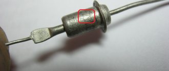
The photo below shows the classic version. Please note that right on the body it is shown where the anode and cathode are. A black stripe is drawn in a circle (more rarely, a gray stripe is found), which is located on the cathode side. The opposite side is the anode. This method is used for both domestic and imported diodes.
Marking the location of the cathode and anode
Adjustable Zener Diodes
When manufacturing stabilized power supplies, the necessary zener diode may be missing. In this case, an adjustable zener diode circuit is assembled.
The required voltage of the stabilizing diode is selected using resistor R1. To configure the circuit, a variable resistor with a nominal value of 10 kOhm is connected in place of resistor R1. After obtaining the required voltage value, determine the resulting resistance and install a resistor of the required value in a permanent place. For this circuit, you can use transistors KT342A, KT3102A.
Marking methods
On the body of the part there is an alphabetic or alphanumeric marking that characterizes the electrical properties and purpose of the device. There are two types of markings. Parts in a glass case are marked in the usual way. The stabilization voltage is written on the surface of the element using the letter V, which acts as a decimal point. The marking of four numbers and a letter at the end is less clear. It can only be decrypted using a datasheet.
Another way to designate stabilizing diodes is by color coding. The Japanese version is often used, which consists of two or three colored rings. If there are two rings, each of them represents a specific number. If the second ring is applied in double form, this means that a comma must be placed between the first and second digits.
How to distinguish a zener diode from a regular diode
Both of these elements have a similar designation in the diagram. In practice, you can distinguish a zener diode from a regular diode and even find out its rating, if it is no more than 35 V, using a multimeter attachment.
Multimeter attachment circuit
To implement a pulse-width modulation generator, a specialized MC34063 microcircuit is used. To ensure galvanic isolation between the power supply and the measuring part of the circuit, the voltage is controlled on the primary winding of the transformer. This allows you to make a rectifier on VD2. The output voltage stabilization point is set using resistor R3. The voltage on capacitor C4 is approximately 40 V. Current stabilizer A2 and the reference diode being tested constitute a parametric stabilizer, and a multimeter connected to the terminals of the circuit allows you to determine the voltage of the zener diode.
If the diode is connected in reverse polarity (anode to “-” and cathode to “+”), then the multimeter for a conventional diode will show 40 V, and for a zener diode - stabilization voltage.
To determine the performance of a zener diode with a known rating, a simple circuit is used, consisting of a power source and a current-limiting resistor of 300...500 Ohms. In this case, a multimeter is used to determine not the junction resistance, but the voltage. Switch on the elements as shown in the diagram and measure the voltage on the zener diode.
Slowly increase the voltage of the power supply. At the value of the stabilization voltage, the voltage on the zener diode should stop growing. If this happens, it means the element is working. If, with a subsequent increase in the IP voltage, the diode does not begin to stabilize, it means that it is not working properly.
How to check zener diode
You can check the zener diode for serviceability quite simply and quickly using a simple multimeter. To do this, the multimeter should be switched to the “continuity” mode, usually indicated by a diode sign. Then, if we touch the anode with the positive probe of the multimeter, and the cathode with the negative probe, then on the display of the measuring device we will see a certain value of the voltage drop across the pn junction. Since direct voltage is applied to the semiconductor device (see the direct branch of the current-voltage characteristic), the reference diode will open.
Now, if the probes of the multimeter are swapped, thereby applying reverse voltage to the terminals of the semiconductor device (see the reverse branch of the current-voltage characteristic), then it will be locked and will not conduct current. The meter display will show a unit, indicating infinitely high resistance.
If in both cases the multimeter shows one or rings, then the zener diode is unusable.
How to choose the right zener diode?
Zener diodes are low power stabilizers. Therefore, they must be selected so that the entire load current plus the minimum stabilization current can pass through them without overheating.
To correctly select a zener diode for an electrical circuit, you need to know the following parameters: minimum and maximum input voltage, output voltage, minimum and maximum load current. The stabilization voltage of the zener diode is equal to the output voltage. And it is best to calculate the maximum current that can pass through a zener diode in a particular circuit, and the power dissipation at the maximum current, using an online calculator.
Zener diode power dissipation
The power dissipation of a zener diode Pst characterizes its ability not to overheat above a certain temperature for a long time. The higher the Pst , the more heat the semiconductor device can dissipate. Uin and the smallest values of Rb and In are substituted into the formula below :
There are a number of standard ratings for this parameter: 0.3 W, 0.5 W, 1.3 W, 5 W, etc. The larger Pst, the larger the dimensions of the semiconductor device.