DIP package
DIP ( Dual I n-Line Package ) - a package with two rows of pins on the long sides of the microcircuit . Previously, and probably still now, the DIP package was the most popular package for multi-pin microcircuits. It looks like this:
Depending on the number of pins of the microcircuit, after the word “DIP” the number of its pins is placed. For example, a microcircuit, or more precisely, an atmega8 microcontroller, has 28 pins:
Therefore, its housing will be called DIP28.
But this microcircuit’s housing will be called DIP16.
In order not to count the number of pins each time, you can count them only on one side of the microcircuit and stupidly multiply them by two.
Basically, logic chips, operational amplifiers, etc. were produced in the DIP package in the Soviet Union. Nowadays, the DIP package also does not lose its relevance and various microcircuits are still made in it, ranging from simple analog ones to microcontrollers.
The DIP housing can be made of plastic (which is in most cases) and is called PDIP , as well as ceramic - CDIP . The CDIP's body feels rock-hard to the touch, which isn't surprising since it's made of ceramic.
Example of CDIP enclosure.
There are also modifications of the DIP housing: HDIP, SDIP.
HDIP ( H eat-dissipating DIP ) - heat dissipating DIP. Such microcircuits pass a large current through themselves, so they become very hot. To remove excess heat, such a microcircuit must have a radiator or something similar, for example, like here are two radiator wings in the middle of the microchip:
SDIP ( S mall DIP ) - small DIP. The microcircuit is in a DIP package, but with a small distance between the legs of the microcircuit:
BGA components
BGA technology originated approximately 20 years ago at IBM for internal consumption. The first company to learn from IBM was Motorola, which bought a license from IBM and developed its technology into a package called OMPAC (Overmoulded Plastic Array Carrier). The structure of the BGA component is shown in Fig. 2.
Rice. 2. BGA component in a plastic case
According to this scheme, the crystal is mounted on a mounting substrate made of a composite material with an organic binder (FR-4, FR-5, BT) having a high glass transition temperature. For these purposes, it is preferable to use a material based on BT (Bismaleimid Triasine) with a particularly high glass transition temperature and excellent electrical properties. A NiAu finishing coating is applied to both sides of the substrate, which is universal for microwelding (welding wires from the microcircuit to the substrate) and soldering ball leads.
The crystal is glued to the substrate with a thermally conductive epoxy resin adhesive. In turn, the substrate has elements of conductive heat removal from one side to the other. Some of the ball leads are intended for thermal connections.
Modern standards set the pitch of the grid of matrix leads: 1.5 mm, 1.27 mm and 1.0 mm and the diameter of the ball leads is 0.6 mm. The designs of 50x50 mm substrates allow 2401 pins to be placed on them with a pitch of 1.0 mm.
Chip chips are mounted on a substrate using one of four methods:
- Thermocompression microwelding (wirebonding) is the oldest, most flexible and widely used method (Fig. 2). More than 96% of all microcircuits are still manufactured with its help.
- Attaching crystals to tape media terminals (Fig. 3), or TAB (Tape-automated Bonding). This method is used for automatic mounting of crystals with a small lead pitch onto an intermediate carrier. In addition to the possibility of automating installation, it provides the possibility of preliminary testing of crystals before final installation on the mounting substrate.
- Attaching an inverted crystal (Flip Chip) through ball terminals (Fig. 4). The compactness and improved electrical performance of this interconnection method are helping to expand its application.
Rice. 4. Installation of the microcircuit on the substrate using the inverted crystal method (Flip Chip)
- Connecting the crystal with beam leads (Fig. 5). This method uses technologies for thermocompression and ultrasonic microwelding of beam leads to peripheral contact pads on the chip and then beam leads to the substrate.
ZIP housing
ZIP ( Z igzag I n line Package ) - a flat package with pins arranged in a zigzag pattern. The photo below shows the ZIP6 housing. The number is the number of pins:
Well, the case with the HZIP :
We have just looked at the main class of In line Package microcircuits. These chips are designed for through-hole mounting in a printed circuit board.
For example, a DIP14 chip installed on a printed circuit board
and its conclusions on the back side of the board, already without solder.
Someone still manages to solder DIP chips like surface-mount chips (more on them below), bending the pins at an angle of 90 degrees, or straightening them completely. This is a perversion), but it works).
Let's move on to another class of microcircuits - surface-mount microcircuits or so-called SMD components. They are also called planar radio components.
Such microcircuits are soldered onto the surface of a printed circuit board, under printed conductors allocated for them. Do you see the rectangular paths in a row? These are printed conductors or popularly piglets. This is exactly what planar microcircuits are soldered onto.
Number of pins and degree of integration of microcircuits
When mounting crystals on a housing substrate and a housing on a mounting substrate (board), or when directly mounting a crystal on a board, the area used for this inevitably increases. This is caused by the need to allocate a certain physical space to accommodate the pins. And the number of pins follows the general trend of their increase with increasing integration of microcircuits:
where n is the number of pins, q is the coefficient of connectivity of microelements in the structure of the microcircuit, N is the degree of integration of the microcircuit, R is the Renta index [4].
In contrast to the degree of integration, this effect is called the degree of disintegration, which is estimated by the ratio of the density of microelements per mounting area on the board with their density on the chip. For example, if the processor chip has a size of 10x10 mm, and the mounting field of its case on the board occupies an area of 4000 mm, this design of the interconnection system is characterized by disintegration with the number 40. What value is estimated for a matrix of 800 pins? The peripheral location of such a number of pins with a pitch of 0.4 mm occupies an installation field with an area of 8000 mm, which means that the degree of disintegration of such a design is 100.
It should be noted that the degree of disintegration increases as the hierarchical level of the design increases: crystal - microcircuit - printed circuit assembly - module - block... For example, disintegration in a block can reach 100 thousand.
Table 2 shows data on a rough assessment of disintegration when using various methods of packaging and installing processor chips on a mounting base (board).
Table 2. Estimation of disintegration when moving to the next level of interconnections
It is obvious that the degrees of integration and disintegration must correspond to the technical level of production development. If you try to complete the design at the maximum production capabilities, the cost of the product will become unreasonably high due to the large amount of scrap waste. The reliability of such structures will also not be guaranteed. If a product is put into production, designed according to low design standards, that is, with a high degree of disintegration (microcircuit of large dimensions), its high material consumption, low capital productivity (“from a gun to sparrows”) will also have a detrimental effect on its cost.
SOIC package
The largest representative of this class of microcircuits are microcircuits in the SOIC ( S mall - Outline I ntegrated C circuit) - a small microcircuit with pins on the long sides. It is very similar to DIP, but pay attention to its conclusions. They are parallel to the surface of the body itself:
This is how they are soldered on the board:
Well, as usual, the number after “SOIC” indicates the number of pins of this microcircuit. The photo above shows microcircuits in the SOIC16 package.
Imported surface mount integrated circuit packages
When assembling electronic equipment, surface mounting technology SMT (Surface Mount Technology) is often used. Electronic components that are manufactured for surface mounting are called SMD (Surface Mounted Device) components. Below are the most common series of imported integrated circuit packages designed for surface mounting.
SOIC or SO (Small-Outline Integrated Circuit) chip package, also known as SOP (Small-Outline Package)
The chip package has a fairly thin rectangular shape, reminiscent of a DIP package, but is designed for surface mounting. The outward curved leads are located on the two long sides and are soldered to the same side of the PCB where the housing is located. The housing designation indicates the number of pins.
- SSOP - compressed small-sized chip package (Shrink SOP);
- TSOP - thin small-sized package (Thin SOP);
- TSSOP - ultra-thin chip package (Thin Shrink SOP);
- QSOP - square body (Quarter SOP);
- MSOP - reduced size SOP housing (Mini SOP);
- CSOP - ceramic chip package (Ceramic SOP);
- HSOP - body with heat sink (Heat Sink SOP);
- HSSOP - small-sized case with a heat sink (Heat Sink Shrink SOP);
- HTSSOP - thin chip package with a heat sink (Heat Sink Thin Shrink SOP);
- VSOP — miniature case (Very Small Outline Package);
- QSOP - square shaped case (Quarter Size SOP).
QFP (Quad Flat Package) chip package
A square, flat microcircuit body with four rows of pins on the narrow sides, they are curved outward.
There are other variants of this case:
- TQFP - thin chip package (Thin QFP);
- LQFP - low-profile chip package (Low-profile QFP);
- SQFP - compressed QFP package (Shrink QFP);
- VTQFP - ultra thin case (Very Thin QFP);
- HQFP - chip package with a heat sink (Heat Sink QFP).
LCC (Leadless Chip Carrier) chip package
Low profile, square ceramic housing with bottom contacts, designed for surface mounting. The housing designation indicates the number of contacts, for example: LCC16, LCC32, etc.
In this article, for your information, we have provided only some cases of imported microcircuits without detailed drawings.
Attention! When ordering and purchasing microcircuits, you need to pay attention to the type of case, since manufacturers often produce the same microcircuit in different types of cases.
Maxim Shakolin
SOP housing
SOP ( Small Outline Package - the same as SOIC .
SOP housing modifications:
PSOP - plastic SOP housing. Most often this is what is used.
HSOP is a heat dissipating SOP. Small radiators in the middle serve to remove heat.
SSOP ( Shrink S mall O utline Package ) - “shrinked” SOP . That is, even smaller than the SOP housing
TSSOP ( Thin S hrink S mall O utline Package ) - thin SSOP . The same SSOP, but “smeared” with a rolling pin. Its thickness is less than that of SSOP. Basically, microcircuits are made in TSSOP packages, which get quite hot. Therefore, the area of such microcircuits is larger than that of conventional ones. In short, a radiator housing).
SOJ is the same SOP, but the legs are bent in the shape of the letter “J” under the chip itself. SOJ body was named after these legs :
Well, as usual, the number of pins is indicated after the package type, for example SOIC16, SSOP28, TSSOP48, etc.
Brief historical background
The first experiments in creating semiconductor integrated circuits were carried out in 1953, and industrial production of integrated circuits began in 1959. In 1966, production of integrated circuits of medium degree of integration began (the number of elements in one crystal is up to 1000). In 1969, integrated circuits with a higher degree of integration (large-scale integrated circuits, LSI) were created, containing up to 10,000 elements in one chip.
In 1971, microprocessors were developed, and in 1975, very-large-scale integrated circuits (VLSI), containing more than 10,000 elements in a single chip. It is useful to note that the limiting frequency of bipolar transistors in semiconductor integrated circuits reaches 15 GHz or more.
By 2000, integrated circuits are expected to appear containing up to 100 million MOS transistors in a single chip (we are talking about digital circuits). Notation system. The symbol for integrated circuits includes the main classification features.
- The first element is a number corresponding to the design and technological group. The numbers 1, 5, 6 and 7 in the first element indicate semiconductor integrated circuits. Hybrid chips are assigned the numbers 2, 4 and 8. Film, vacuum and ceramic integrated circuits are designated by the number 3.
- The second element, which determines the serial development number of the series, consists of two (00 to 99) or three (000 to 999) digits.
- The third element, indicating the subgroup and type of microcircuit, consists of two letters.
- The fourth element, indicating the serial number of the development of the microcircuit of this series, consists of one or more digits.
It will be interesting➡ All about power supplies - device diagram, DIY production
Other classification features can be added to these basic elements of microcircuit designations.
Structure of an integrated circuit
An additional letter at the beginning of the four-element designation indicates a design feature:
- P - plastic housing type DIP;
- A - plastic planar body;
- E - metal-polymer housing of the DIP type;
- C - glass-ceramic body of DIP type;
- I - glass-ceramic planar body;
- N - ceramic “leadless” housing.
At the beginning of the designation for microcircuits used in widespread use, the letter K is given.
Series of unpackaged semiconductor microcircuits begin with the number 7, and unpackaged analogues of packaged microcircuits are designated by the letter B before the series indication.
A hyphen after the designation indicates a number characterizing the modification of the design:
- 1 - with flexible leads;
- 2 - with strip (spider) leads, including those on a polyamide carrier;
- 3 - with rigid leads;
- 4 - on a common plate (undivided);
- 5 - separated without loss of orientation (pasted on film);
- 6 - with contact pads without leads.
How are integrated circuits created?
How to make a memory chip or computer processor? The manufacturing process begins with the chemical element silicon, which is chemically treated (alloyed) to impart different electrical properties.
A modern design of an integrated circuit (one of many forms) installed on the electronic board of the device. This is far from the most advanced option, but only one of many
Traditionally, materials of two categories are used for electronics needs:
- Conductors.
- Insulators.
But technically, everything is more complicated, especially when it comes to certain elements in the middle of the periodic table (groups 14 and 15), in particular silicon and germanium. What is noteworthy is that insulating materials can become conductors if a certain amount of impurities is added to these materials. A process known as alloying.
The principle of alloying chemical elements
If you add some antimony to silicon, the structure of this chemical element is saturated with more electrons than usual. Conducts electricity. Silicon "doped" in this way takes on the N-type characteristic. In another case, when boron is added instead of antimony, the mass of silicon electrons decreases, leaving peculiar “holes” that function like “negatively charged electrons.”
The holes allow positive electrical current to flow in the opposite direction. This type of silicon is characterized by P-type. Placing N-type and P-type silicon regions next to each other creates a junction that exhibits electron behavior characteristic of semiconductor-based electronic components:
- diodes,
- transistors,
- storage devices and others.
Enlarged photo of integrated circuits
QFP package
QFP ( Q uad F lat Package ) - quadrangular flat body. The main difference from its fellow SOIC is that the pins are located on all sides of such a chip
Modifications:
PQFP - plastic QFP package. CQFP - Ceramic QFP package. HQFP is a heat dissipating QFP package.
TQFP ( T hin Q uad F lat P ack) - thin QFP package. Its thickness is much thinner than its QFP cousin
PLCC housing
PLCC ( Plastic L eaded C hip C arrier) and CLCC ( C eramic L eaded C hip C contacts located along the edges, designed for installation in a special socket, popularly called a “crib”. A typical example is the BIOS chip in your computers.
This is what the “bed” for such microcircuits looks like:
And this is how the microcircuit “lies” in the crib.
Sometimes such chips are called QFJ , as you guessed it, because of the “J”
Well, the number of pins is placed after the name of the case, for example PLCC32.
Variety of integrated circuit packages
Today, integrated circuits are produced in two versions - packaged and unpackaged. A packageless chip is an open chip designed for installation in a hybrid chip or microassembly. To protect them from external influences, integrated circuits are placed in a plastic or ceramic case. Microchip packages are standardized. Engineers often come across English-language documents in which the package of an integrated circuit is called “chip package”, “chip container” or “chip carrier”.
PGA package
PGA ( P in G rid A rray) - a matrix of pin pins. It is a rectangular or square case, in the lower part of which there are pins.
Such microcircuits are also installed in special cribs, which clamp the terminals of the microcircuit using a special lever.
PGA packages are mainly used to make processors for your personal computers.
Parameters of digital microcircuits
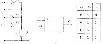
Before talking about the parameters of digital logic chips, it is necessary to say that not all of them are taken into account and not always. How can you ask a question? But it’s very simple here; when developing and modeling digital devices, we start from various models of logic chips. There are three such models in total:
1. Logic model.
2. Model with time delays.
3. Electric model.
For logic model
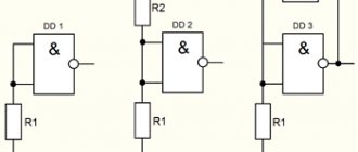
everything is very simple, here the main parameter is the truth table or description of the algorithm of operation of the logical element. Approximately 20% of all circuits are based on a logic model. In this model, we can assume that the logic element operates instantly.
For a model with time delays
it is necessary to take into account that the output signal changes with some delay relative to the input signal. This model allows you to develop about 80% of all devices. This model takes into account the parameters of the delay during the transition of a signal from one to zero (tPHL) and the transition of a signal from zero to one (tPLH).
For electric model
The logic chip already takes into account input and output currents, as well as input and output voltages. This model suggests that voltage and current levels are not set instantly, but taking into account transient processes inside the microcircuits. All other digital devices are developed with this model in mind. Here are some of them: zero input current (IIL) and one input current (IIH); zero input voltage (UIL) and one input voltage (UIH); zero output current (IOL) and one output current (IOH); output voltage zero (UOL) and output voltage one (UOH).
Also for digital logic chips there are general electrical parameters: permissible supply voltage (UCC) and maximum current consumed by the chip (ICC).
LGA case
LGA ( L and G rid A rray) is a type of microcircuit package with a matrix of contact pads. Most often used in computer technology for processors.
The crib for LGA chips looks something like this:
If you look closely, you can see spring-loaded contacts.
The chip itself, in this case the PC processor, simply has metallized pads:
In order for everything to work, a condition must be met: the microprocessor must be pressed tightly to the crib. Various types of latches are used for this.
Structured integrated circuit inside a chip
So, the process of creating an integrated circuit begins with a single silicon crystal, shaped like a long solid pipe, “cut” into thin disks - plates. Such wafers are laid out into many identical square or rectangular areas, each of which represents one silicon chip (microchip). An example of the internal structure of an integrated circuit, demonstrating the capabilities of such a unique technology for integrating full-fledged electronic circuit solutions.
It will be interesting➡ All about power supplies - device diagram, DIY production
Thousands, millions, or even billions of components are then created on each chip by doping different areas of the surface into N-type or P-type silicon. Alloying is carried out in various ways. One option is sputtering, when a silicon wafer is “bombarded” with ions of the dopant material.
Another option is vapor deposition, which involves introducing an alloying material in the gas phase followed by condensation. As a result of this introduction, impurity atoms form a thin film on the surface of the silicon wafer. Molecular beam epitaxy is considered the most accurate deposition option.
Of course, the creation of integrated circuits, where hundreds, millions or billions of components are packed into a silicon chip the size of a fingernail, seems to be a very complex process. One can imagine what chaos even a small grain will bring when working on a microscopic (nanoscopic) scale. This is why semiconductors are manufactured in squeaky clean laboratory conditions. The air in laboratory rooms is carefully filtered, and workers must pass through protective airlocks and wear protective clothing.
Interesting read: what are klystrons.
Who created the integrated circuit?
The development of the integrated circuit is credited to two physicists, Jack Kilby and Robert Noyce, as a joint invention. However, in fact, Kilby and Noyce hatched the idea of an integrated circuit independently of each other. There was even a kind of competition between scientists for the rights to the invention.
Jack Kilby was working at Texas Instruments when the scientist managed to realize the idea of a monolithic principle of placing various parts of an electronic circuit on a silicon chip. The scientist manually created the world's first integrated circuit (1958), using a germanium-based chip. a year later she filed a patent application.
Meanwhile, a representative of the other, Robert Noyce, conducted experiments with miniature circuits of his device. Through a series of photographic and chemical techniques (the planar process), Kilby created a practical integrated circuit just a year later. The production method was also filed for a patent.
Microcircuits on the board