Logic elements were invented to perform logical operations and solve logical problems using electronics. They are created using diodes, transistors and combined elements (diode-transistor). This logic is called diode logic (DL), transistor logic (TL) and diode-transistor logic (DTL). Both field-effect and bipolar transistors are used. In the latter case, preference is given to npn type devices, as they are faster.
Logic element "OR"
The diagram of the “OR” logic element is shown in Figure 1 a. Each input can receive a signal in the form of some voltage (one) or its absence (zero). Voltage will appear across resistor R even if it appears on any of the diodes.
Rice. 1
Elements or can have several logical inputs. If not all inputs are used, then those inputs that are not used should be connected to ground (grounded) to avoid the appearance of extraneous signals.
Figure 1b shows the designation on the electrical circuit of the element, and 1c shows the truth table.
Boolean functions
Using this calculator, a truth table is built using a Boolean function, the properties of the function and other parameters are determined (see the Solution parameters tab).
In this case, only the logical expression itself is entered without a prefix. For example, when f(x,y,z) = x → y!z, you only need to enter x → y!z. The entered expression can also be simplified using the laws of propositional logic (in the next step, select the Simplify expression option). (...) - entering parentheses, x - negation (NOT, !, ¬), & - logical AND, AND, ∧, *, v - logical OR, OR, ∨, = - equivalence, ˜, ≡, ↔, ⊕ - sum modulo 2, | - Schaeffer's stroke, AND-NOT, AND-NOT, ↓ - Pierce's arrow, OR-NOT, OR-NOT, ← - inverse implication.
For nested negation you must use the ! sign. For example, xvy = !(xvy) or xvy = xv !y
Using the found truth table, you can determine the logical values of statements, for example, at x=0, y=0, z=1. To check a statement for truth or falsity, the function must be entered without the equal sign (=). For example, A+B→A&B=1, you need to enter A+B→A&B. If as a result of the transformations it turns out that f = 1, then the statement is true, if f = 0, it is false.
Logical (functional) elements {v,&, ¬} are the most common: due to the completeness of the system, any
Boolean function (BF) can be represented as a superposition of disjunction, conjunction and negation.
Any Boolean functions can be considered as functional elements (FE), and they can be connected to each other, feeding the outputs of some elements to the inputs of others (superposition of BFs). The domain of definition of the BF E is a finite set, so the BF can be specified using a truth table containing |E|=2n rows. The BF value column is a binary word of length 2n. Therefore, the number of different BF n variables is 22n.
Denial, ¬
xf 0 1 1 0
Conjunction, &
xyf 0 0 0 0 1 0 1 0 0 1 1 1
Disjunction, v
xyf 0 0 0 0 1 1 1 0 1 1 1 1
Sum modulo 2, x⊕y
xyf 0 0 0 0 1 1 1 0 1 1 1 0
Pierce's arrow, x↓y
xyf 0 0 1 0 1 0 1 0 0 1 1 0
Equivalence, x↔y
xyf 0 0 1 0 1 0 1 0 0 1 1 1
Implication, x→y
xyf 0 0 1 0 1 1 1 0 0 1 1 1
Schaeffer stroke, x|y
xyf 0 0 1 0 1 1 1 0 1 1 1 0
Other BFs are constructed from elementary ones using superpositions of functions.
Basic equivalences of propositional logic
| Name | Formula |
| Law of the excluded middle | X v !X ≡ And |
| Law of contradiction | X & !X ≡ L |
| Commutativity law | X & Y ≡ Y & XX v Y ≡ Y v X |
| Law of associativity | (X & Y)&Z ≡ X&(Y&Z) (X v Y) v Z ≡ X v (Y v Z) |
| Distributivity law | X&(Y v Z) ≡ X&Y v X&Z X v Y&Z ≡ (X v Y)&(X v Z) |
| Law of double negation | !!X ≡ X |
| Law of Idempotency | X&X ≡ X, X v X ≡ X |
| De Morgan's laws | !(X v Y) ≡ !X & !Y !(X & Y) ≡ !X v !Y |
| Law of Absorption | X v X&Y ≡ X X&(X v Y) ≡ X |
| Laws of gluing | (X & Y)v(X & !Y) ≡ X (X v Y)&(X v !Y) ≡ X |
| Replacement of implication | X → Y ≡ !X v Y |
| Replacement Equivalence | X = Y ≡ X&Y v !X&!Y |
Example. Simplify the expression: (x˅y˅z)→(x˅y)*(x˅z) Let’s simplify the function using the basic laws of propositional logic. Replacing the implication: A → B = !A v B For our function: (xvyvz)→((xvy) (xvz)) = xvyvzv (xvy) (xvz) Let’s simplify the function using de Morgan’s laws: !(A v B) = !A & !B For our function: xvyvz = xyz According to the distributive law: (xvy) (xvz) = xvxzvyxvyz we obtain: f = xyzvxvxzvyxvyz After elementary transformations we obtain: f = xyzvxvxzvyxvyz = xyzvxvyzf = yzvyzvx
Logic gate "AND"
The element diagram is shown in Fig. 2. If at least one of the inputs has a signal equal to zero, then current will flow through the diode. The voltage drop across the diode tends to zero, and accordingly the output will also be zero. A signal can appear at the output only if all diodes are closed, that is, there will be a signal at all inputs. Let's calculate the signal level at the device output:
Fig.2
in Fig. 2 b – designation on the diagram, c – truth table.
Logic element "NOT"
A transistor is used in the “NOT” logic element (Fig. 3 a). when there is a positive voltage at the input x=1, the transistor opens and its collector voltage tends to zero. If x = 0, then there is no positive signal at the base, the transistor is closed, the current does not pass through the collector and there is no voltage drop across the resistor R, respectively, signal E will appear on the collector. The symbol and truth table are shown in Fig. 3 b, c.
Fig.3
Minimizing Boolean Functions
This service uses the Quine method and Karnot-Veitch maps to minimize Boolean functions. After obtaining the minimum form, it is possible to rebuild the logical circuit. If the original scheme is needed in the future, it can be saved first (menu Actions/Save).
The BF can be reduced by applying some equivalences of propositional logic:
- Kx v K ≡ K—absorption identity;
- Kx v Kx ≡ K—gluing identity;
- Kx v Ky ≡ K(xvy) - distributive law,
where K is an elementary conjunction. Most BF minimization methods are based on the first two identities. And the third - the distributive law - reduces the number of letters in the formula, but removes the formula from the DNF class. When minimizing BFs, different terms (and designations) are used for complete elementary conjunctions (PECs). The most commonly used terms are “minterm” and “unit constituent”. (For complete elementary disjunctions (PED), the terms “maxterm” and “constituent of zero” are used). The word “constituent” means “component”, and the name “minterm” comes from the definition of a conjunction as the minimum value of its operands. In this case, the designations mi are used for minterm and Mi for maxterm. Number i corresponds to the binary notation of the variable estimate for which mi=1.
Karnaugh map method
You can merge either the entire map or only selected units (Operations menu).
- Merge selection
- Glue the entire map
- Remove splices
- Save as docx
- Save as png
- ✍ Help in solving problems
Number of variablesGrid
After minimization, you can obtain a logical diagram of the function and build a truth table (Next button)
This method is used for BF with no more than six arguments and is based on the gluing identity: Kx v Kx ≡ K - two elementary conjunctions (EC) are glued if they differ only in the sign of the inversion of one argument. To make it easier to find such pairs (fours, eights,...) of sticking ECs, use a special representation of the BF in the form of a table - a Karnaugh map (another name is a Veitch diagram) . To fill out a Karnaugh map, you need to left-click on the corresponding cell. The Karnaugh map has the peculiarity that two PECs corresponding to adjacent cells of the map differ in the inversion sign of only one argument, i.e. they can be glued together. Moreover, not only cells, for example, with numbers 1 and 3, but also cells with numbers 12 and 8, 12 and 4, are neighboring, i.e. the map can be “rolled” into a cylinder, connecting its horizontal (vertical) borders. Two units are "stuck" whenever they are adjacent in a row or column (the card can be rolled into a cylinder). As a result of gluing, the number of letters included in the PEC is reduced by one.
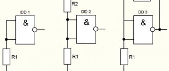
Logic element "OR-NOT"
When creating various circuits using logical elements, combined elements are often used. Such elements combine several functions. The schematic diagram is shown in Fig. 4 a.
Fig.4
Here diodes D1 and D2 play the role of an “OR” element, and the transistor plays the role of an inverter. Designation of the element in the diagram and its truth table Fig. 4b and c respectively.
Minimizing functions through equivalent transformations
see table of equivalent transformations
Algorithm for minimizing a logical function
- Replacing implication and equivalence.
- Simplification of a function through De Morgan's laws.
- Opening brackets using the laws of absorption, excluded middle, contradiction.
- Minimization through the law of distributivity.
Quine's algorithm for constructing a reduced DNF
- Get SDNF functions.
- Carry out all partial gluing operations.
- Carry out all acquisition operations.
Logic element "AND-NOT"
The diagram is shown in Fig. 5 a. Here diode D3 acts as a filter, so to speak, to avoid signal distortion. If no signal is applied to input x1 or x2 (x1=0 or x2=0), then current will flow through diode D1 or D2. The drop across it is not zero and may be sufficient to open the transistor. The consequence may be a false positive and at the output we will get zero instead of one. And if D3 is included in the circuit, then a significant part of the voltage of the diode open at the input will drop across it, and practically nothing comes to the base of the transistor. Therefore, it will be closed, and the output will be one, which is required if there is a zero at any of the inputs. In Fig. 5b and c show the truth table and circuit designation of this device.
Fig.5
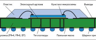
Logic elements are widely used in electronics and microprocessor technology. Many control systems are built using these devices.
(i.e., they allow you to place a larger number of logic elements in one integrated module) and do not require the use of stabilized power supplies.
Transistor-transistor logic gates (TTL)
TTL elements are used in integrated circuits and provide high switching speed. In Fig. Figure 34.1 shows a simplified circuit of a NAND gate with multi-emitter transistor T1 at the input. When both inputs are logic 0, transistor T1 is saturated and its collector voltage is close to 0 V. Therefore, transistor T2 is in cut-off state and the output is logic 1. When both inputs are logic 1, transistor T1 turns off and switches transistor T2 into saturation state. In this case, we have a logical 0 at the output of the element.
Rice. 34.1. Logic element AND-NOT (TTL type).
Logic elements based on field-effect transistors
Logic circuits are currently manufactured only as integrated circuits. A huge number of logic elements can be placed on the smallest silicon crystal (chip) measuring 1x2 mm. Due to their simplicity, field-effect transistors are used more often than bipolar transistors. The most widely used logic elements are based on so-called CMOS cells (they are not discussed here). In Fig. Figure 34.2 shows a diagram of a NOR logic element based on MOS transistors, which operates on the basis of negative logic. In this circuit, T1 and T2 are MOSFETs with channel p
-type (operating in enrichment mode).
When both inputs have a logical level of 0, transistors T1 and T2 are in the cutoff state and we have a logical 1 at the output (- V
DD= -20 V). When a logical 1 is applied to one or both inputs (for example, -20 V), one or both transistors open and we get a logical 0 at the output.
Rice. 34.2. Logic element Fig. 34.3. Logic element based on NAND
NOR-NOT on MOSFETs. MOSFET transistors.
In Fig. Figure 34.3 shows a diagram of an AND-NOT logic element based on MOSFETs with channel n
-type.
Since a positive polarity power supply is used, this logic element operates on the basis of positive logic. Transistor T3 is constantly biased into the active operating region by the voltage V
DD applied to the gate, and acts as an active load for the logic element. When one or both inputs are logic 0, one or both transistors are in the cutoff state, producing a logic 1 output. Current will flow through the transistors only if a logical 1 is applied to both inputs, and only in this case will we receive a logical 0 at the output.
Boolean Expressions
The functions implemented by an individual logic gate or combination of logic gates can be expressed by logical formulas called Boolean expressions. In Boolean algebra, the following notations for logical functions are used (see Table 34.1):
• The AND function is represented by the dot symbol (·). A two-input (inputs A and B) AND gate produces an output signal represented by the Boolean expression A · B .
• The OR function is indicated by a (+) symbol. A two-input OR gate produces an output signal represented by the Boolean expression A + B.
Table 34.1. Boolean Expressions
| Function | Notation in Boolean algebra |
| AND | A·B |
| or | A+B |
| NOT | |
| AND-NOT | |
| OR NO | |
| Exclusive OR | |
| Exclusive OR NOT |
• A Boolean function is NOT indicated by a bar symbol above the input signal symbol. A NOT logic circuit with one input A produces an output signal represented by a Boolean expression (read “NOT A”).
More complex ones can be expressed through these simple functions:
•
The H-NOT function is written as
.
•
The OR-NOT function is written as
.
• The Exclusive OR function is written as .
It can also be written using a special notation,
.
• The Exclusive OR NOT function is written as .
It can also be written using a special notation,
.
Combinatorial logic
Consider the logical circuit in Fig. 34.4. The logical function performed by this circuit can be described using the following Boolean expressions.
OR gate output (i): A + B
Output signal of I-IE gate (ii):
OR gate output (iii): (A + B) +