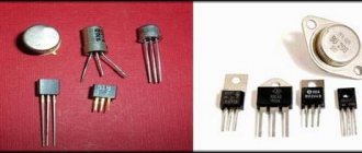
Principles of operation of field-effect transistors in electronic circuits: simplified information
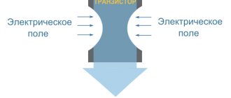
It is convenient to imagine all complex electronic processes using the example of an ordinary water tap with a handle that allows you to turn off the water or regulate its pressure from a very thin trickle (flow) to the strongest possible flow.
I showed this with a primitive picture in which:
- the inlet pipe with pressure is called drain;
- the place of water outlet (outflow) is indicated by the source;
- control handle or valve with a rod - shutter.
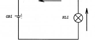
The electrical circuit of the field-effect transistor we are considering works in a similar way. Only it has the main constant voltage applied between the drain and source. This area is called a channel. It is made of a semiconductor of a certain structure:
- n-type (electrons predominate - carriers of negative charges);
- p-type - with an excess of positive holes.
In the drawings, these conclusions are shown in one of the following images.
On the shutter designation, we need to pay attention to the direction of the arrow. For n-channel semiconductors it is directed towards the gate, and with p-conductivity it is directed in the opposite direction.
Any field-effect transistors are semiconductors, and controllable ones at that. This means that it passes a load through itself exclusively in one direction, and the opposite movement of electrical charges is always blocked.
The movement of current through semiconductor junctions is always directed from drain to source, just like water in a tap. This is important to remember.
The functions of closing or opening this tap (gate), as well as the role of regulating the force of the flow of electrical charges, are assigned to the gate. Ohm’s well-known law applies here:
I=U/R
The resistance of the channel medium controls the load, and it is acted upon by an externally applied potential.
In other words: the electric field energy applied to the gate changes the resistance of the internal semiconductor junctions and affects the amount of current in the output power circuit.
The word “field” is significant here. It has defined a number of transistor products operating according to this control principle.
The electric field potential controls the amount of resistance across the power semiconductor layer (channel), turning the transistor off/on or changing the current through it.
Bipolar transistors (BTs), about which a previous article was published on my blog, are controlled in a similar way.
Only in them the power circuit is formed between the collector and the emitter, and the control circuit operates from the current generated by the application of voltage between the base and emitter. BT has its own pin designation system, but the same two internal circuits (power circuit and its regulation circuit).
I would like to draw your attention: at the same voltage between the input and output of the field-effect transistor (drain-source), the potential at the gate changes the electrical resistance of the built-in semiconductor junctions.
Moreover, this happens according to one of the scenarios provided in advance. I talk about them successively further.
What is it needed for
PTs are needed to control the output current using the generated electric field and change its most important parameters. Structures based on field-effect transistors are often used in digital and analog integrated circuits.
n- and p-channel electrotransistors
It is through field control that these transistors influence the magnitude of the voltage applied to their gate. This distinguishes them from bipolar transistors, which are controlled by the current that flows through their base. PTs consume significantly less electricity, which determines their popularity when used in waiting and tracking devices, as well as low-consumption integrated circuits (when organizing sleep mode).
You may be interested in this The danger of step tension
Important! Some of the most famous devices based on the action of field-effect transistors are TV remote controls and electronic wristwatches. Due to their design and the use of DC, these devices can operate for years from one tiny power source in the form of a battery.
Schematic view of a field-effect transistor
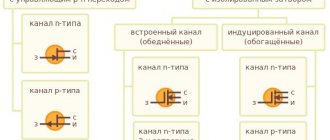
How a field-effect transistor works: 6 types - brief information
The classification shown in the picture below, where their types are structured, will help us deal with a specific field grass and understand its structure.
JFET and MOSFET have different structure. In JFET, the gate (Gate) is directly built into the cross section of the channel and works as a control pn junction.
For mosfet:
- there is an additional fourth pin connected internally to the housing. It is not used when connecting to external circuits;
- The gate output region is separated by a layer of silicon dioxide (dielectric) from the channel semiconductor. It works as a plate capacitively coupled capacitor. Due to this modification, it is called an “insulated gate” or MOS transistor.
MIS stands for metal-dielectric-semiconductor and MOS stands for metal-oxide-semiconductor. The difference between them for a novice electrician is not significant, practically absent.
In the diagrams, mosfet and jifet are designated in different ways. MOSFET is drawn with:
- the fourth pin, which is not connected anywhere;
- a shutter separated from the main channel.
Mosfets are manufactured with different substrates (channels), which can be depleted or enriched in major charge carriers.
I will not describe and describe in more detail the differences between each type of these semiconductors for a novice electrician: there is not much point.
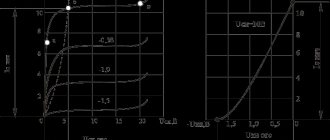
Below are just typical schedules of their work. They will give a general idea of behavior, and you will need to take specific data from the datasheet - technical documentation.
The amount of current flowing through the drain depends on the applied voltage between gate and source, as well as the ambient temperature.
The output drain current characteristics depend on the magnitude of the applied voltage between drain-source and gate-source.
This is how a MOS transistor with a built-in channel works. The current slope increases with increasing voltage Usi, Uzi.
And here are the characteristics of transistors with an induced channel.
Before any check of each transistor, it is necessary to clarify its technical capabilities according to the factory documentation.
Such graphical images and dependencies of electrical engineering processes, due to their clarity, have better information content.
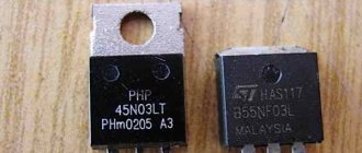
6 features of electronic devices using MOSFETs
Recently, we are increasingly working with mosfet-type field devices with a channel of any conductivity.
Let us briefly analyze such a scheme and its properties.
Point No. 1: which shoulder to place the load on?
When the semiconductor junction is completely open, a very small resistance of tens or hundreds of milliOhms (Ropen) is created between the drain and the source, which forms a low voltage drop in this section (In · Roopen), where In is the value of the load current.
The voltage potential applied to the gate may not be sufficient to fully open the semiconductor. Therefore, the load is turned on higher on the drain side in an n-type field switch, and on the source side in a p-type field switch when the circuit is powered from a single source.
If the device uses additional voltage sources, then this requirement is not necessary.
Point No. 2: tricks for connecting a field worker to microcontrollers
For reliable operation of the MOSFET, it is necessary to apply a threshold voltage value between its gate and source (gate-source), which is indicated in the datasheet. It is usually around 10 volts. Still, digital devices work up to five: their power supply is not enough, you will need to add a level.
You can solve the problem in one of three ways:
- a key with bipolar transistors supplies the necessary power to the gate;
- connect a special driver (chip) to generate a control signal. They are designed for both the upper and lower shoulder to accommodate the load. Moreover, the high-side driver often uses a circuit to increase the output voltage;
- use a specialized low-level field operator (logic level). However, acquiring it can be problematic.
Point No. 3: how to avoid the influence of electrical interference
The appearance of any interference potential at the output of a transistor often leads to its unauthorized switching and disruption of electronic operating algorithms.
Therefore, the gate is always “pulled” to power or ground through a certain resistance, even when connected through a microcontroller. It should not be left in a free state, accessible to the penetration of extraneous interference.
Point No. 4: combating surge current when turned on
The natural presence of capacitance at the gate pin leads to a “current surge” each time the transistor is turned on. This can lead to damage to the semiconductor junction.
The problem is solved by introducing a resistor of sufficient value into the gate circuit. However, its value must be selected taking into account the increase in the key opening time.
Feature No. 5: inrush current protection when disconnecting inductive loads
A protective high-speed TVS diode, connected in parallel between the source and drain, reliably shunts the pulses created by disconnecting inductive loads.
When operating at high frequencies in bridge or half-bridge circuits of switching power supplies or induction heaters of hobs, a Schottky diode is connected counter-currently to the drain output, blocking the parasitic diode, because it increases the closing time, which can damage the semiconductor.
Point No. 6: additional MOSFET
Safe operation of a high-speed high-frequency switch in the switching mode of powerful inductive loads is ensured by its connection to snubber circuits. They:
- aperiodic currents created by transient processes close on themselves;
- reduce heating of semiconductors;
- protect the field switch from unauthorized opening during a rapid increase in voltage between drain and source.
Breakdown of the collector-emitter junction
If “current” causes of failure provide time to make a decision on protection, then overvoltage does not provide such time, since it only takes a few nanoseconds for a transistor to fail, and during that time no protection will have time to connect. Therefore, overvoltage should be combated with preventive measures. There are two main ways of fighting: active and passive. Active implies control of the transistor in such a way that voltage surges are minimized; This includes soft shutdown. Active protection, as a rule, is connected as needed, which means it does not lead to an increase in dynamic losses in normal operation, but is inferior in speed and ease of implementation to passive protection. Passive protection, unlike active protection, is always enabled, regardless of whether it is needed at the moment or not. This protection is implemented in two ways: dU
/
dt
and limit. The first includes various kinds of snubbers, the second - limiters and varistors. Next in order.
Passive protection: snubbers
In the simplest case, a snubber is just a capacitor. And, as practice shows, RC and RCD snubbers do not have any significant advantages over a single capacitor. The capacitor, in turn, is subject to a number of requirements: it must be installed as close as possible to the power terminals of the collector and emitter of the transistor module; if you put it “somewhere” on the bus, the efficiency will be significantly less. At one time, an experiment was carried out: with a capacitor installed inside the module, at a supply voltage of 550 V and the inverter operating at a load of 5.5 kW, surges with an amplitude of up to 650 V were observed; when the capacitor was installed only on the power buses (connection “soldering busbars – module busbars – screw fastening – power busbars”), the emissions increased to almost 800 V. Of course, the capacitor is the same, the modes are the same. In addition, it is very desirable that the capacitor is not screwed, but soldered, since fastening with a clamp also significantly reduces the efficiency of the snubber. Its efficiency also decreases if the capacitors are installed in series (due to an increase in parasitic active resistance) or in parallel, since three 0.1 µF capacitors are not equivalent to one 0.33 µF; The best option is to install a single capacitor.
Quantity
If the converter has several modules, then the number of capacitors should not be the same as the number of power transistors. The number of snubbers is determined more by the topology of the converter's power circuit than by the electrical circuit diagram itself. The simplest example is several transistors connected in parallel. If the power buses are routed correctly, namely: the buses are wide, the “+” and “–” buses are located one below the other, the distance between the power modules is minimal, then one snubber (for example, 0.1 uF) installed on the power buses is sufficient. If the distance between the modules is relatively large, and the connection between them is carried out by wires (especially if the cross-section of these wires is insufficient), then it is necessary to install snubbers on each module, and, under the same other conditions, the nominal value of each snubber should also be 0.1 μF. This is explained by the fact that a snubber, in its essence, is designed to “clean” the power supply, and if the parasitic inductances of the connections of individual power points are minimal, then there is no need to “clean” each point separately. And vice versa: if the inductance of the connections is high, then each power point must be “cleaned” separately. The same rule applies to the scheme itself. For example, as experiments have shown, there is no difference between one snubber installed on the power buses of a three-phase inverter and a circuit where capacitors are in parallel with each transistor. Of course, the difference will be in the ratings, but since it was possible to achieve emissions of 50 V at best, there is no point in increasing the dimensions of the circuit. In general, it is better to focus on topology rather than on the number of snubbers and increasing dimensions.
Types
As for the type of capacitor, in the vast majority of cases the usual K73-17 is sufficient, and sometimes even K10-17. Having no experience with specialized imported capacitors, I cannot say whether “they” have much better capacitors, however, comparing with domestic low-inductance and specialized capacitors, I was convinced that there is practically no difference between them and K73-17. But there is a difference between mounted and SMD capacitors. At one time, an attempt was made to replace the mounted capacitor with an SMD of the same type and rating. As a result, if for many years before there had not been a single failure of a mounted capacitor, then SMD capacitors exploded in two out of three emergency situations and, as a result, they had to be abandoned. Detailed checks on this matter have not been carried out, so it is difficult to say what exactly the problem is: overvoltage resistance, pulse power or something else, but the fact is obvious.
Options
Of course, the capacitance must be calculated according to the inductances, both load and parasitic, but, as practice shows, the value of the snubber capacitor almost always remains the same, at least in the field of controlling motors of various types with power from hundreds of watts to tens of kilowatts. This is 0.1–0.4 μF (optimally 0.22 and 0.33 μF), regardless of motors, modes, voltage, etc. Moreover, further increase in capacitance is ineffective; changing the nominal value from 0.1 µF to 0.33 µF gives a gain in voltage pulse suppression of up to 50%, and increasing the capacitance by another order of magnitude (up to 3.3 µF) in the best case will give 10–20%, and then suppression completely will begin to decrease.
Passive protection: limiters and varistors
Let's move on to the second type of passive protection: limitation. If the purpose of a snubber is to reduce dU
/
dt
and, thereby, reducing the peak amplitude of the voltage surge, then the meaning of the limitation is to “cut off” the voltage at a set level. For these purposes, either voltage limiters or varistors are used. The latter have not been widely used for transistors due to low performance, but limiters are used very widely.
Recommendations for installing limiters are similar to those for snubbers. They can be dialed in series (but not in parallel), and this method is convenient not only for selecting the required voltage, but also for increasing the maximum power. For example, four 1.5 kW, 200 V limiters will be twice as powerful as two 400 V limiters, although their rated breakdown voltage will remain the same. The rated breakdown voltage of the limiter should be selected based on the rule that it should be 30% higher than the rated supply voltage and 30% lower than the maximum permissible collector-emitter voltage of the transistor. Deviation from this point in one direction or another depends on what is more critical: either overheating of the limiters (and this implies an increase in size), or the risk of breakdown of the power transistor.
The good news is that low-inductance, powerful high-voltage limiters for special purposes have finally appeared (manufactured by NZPP, Novosibirsk), which greatly simplifies the design of power devices.
However, limiters have the disadvantage that their performance is not ideal; As a rule, their response delay ranges from one to several tens of nanoseconds. And sometimes it's a lot. Modern transistors are quite capable of creating a turn-off duration of 20–30 ns, which means that, for example, with a 600 V supply and an 800 V limiter, the duration of the voltage rise from 800 to 1200 V (breakdown for the transistor) will be less than 10 ns; The limiter will not have time to open before the power transistor fails. Therefore, the turn-off duration of the transistor should be no less than 50 ns, and preferably 100 ns. Therefore, if you do not “prepare” the circuit by reducing dU
/
dt
, then the limiters will be of no use.
reduce dU
/
dt
either with the same snubber, or by delaying the switching off of the control pulse. Then and only then will the limiter be able to protect the power transistor.
Soft shutdown
The easiest way to actively combat overvoltage is to smoothly turn off the transistor. Let's first consider a smooth shutdown, which is always present, regardless of whether the control driver has switched to an emergency mode (due to a transistor load short circuit) or not; the short circuit mode and its inherent smooth shutdown will be discussed in the second part. As a rule, in order to form a smooth switch-off, a gate switch-off resistor of a relatively large value is installed. As a consequence, there is a prolonged resorption of the gate capacity and, thus, a lower turn-off speed. This practice of increasing the shutdown duration is generally accepted, however, if the driver is not purchased, but is developed in-house, then you can use a little trick: it is better to form a smooth shutdown before the final stage of the driver (if this stage is assembled on bipolar transistors) by installing a charging capacitor in the base of the transistors (turn on) through a diode, and the discharger (turn off) through a resistor. In terms of rise time, this will not change anything, but the output impedance of the driver will significantly decrease, which means that noise immunity and dU/dt
drivers in static locking mode. But this is by the way.
The rise time, regardless of operating modes and type of transistor, should ideally be 1–3 μs; it is possible, if the load really requires it, to expand this range to 0.5–5 μs. If you continue to reduce the shutdown duration, then it will no longer be a smooth shutdown, and if you increase it, there will be practically no improvement either, only dynamic losses will increase. Of course, sometimes dynamic losses or a high switching frequency do not allow the fronts to be delayed so much, but then this method simply is not suitable, and nothing can be done about it. But if losses are acceptable, then it is better to play it safe and make a decline of at least 1 μs. In this case, the duration of the decline should be measured relative to 0 V, and not relative to the negative voltage. That is, if the transistor is controlled by a voltage of +15/–10 V, then those same 1–3 μs should pass when transitioning from +15 V to 0 V, and not to –10 V; shutdown down to –10 V can last twice as long. This reference point is explained by the fact that the transistor is guaranteed to turn off at a voltage of 0 V, and it is indifferent to what the voltage at its gate will look like next; This is just the “tail” of the control circuit, and nothing more. By the way, previously for drivers (for example, old Mitsubishi drivers) smooth shutdown was standardized at levels of 90–50 and 90–10%, but now it is customary to declare only the latter value.
"Active" protection
“Active” protection (active clamping) is perhaps the most complex circuit solution for implementing overvoltage protection for a power transistor. In this case, we mean a circuit in which the “excess” voltage from the “collector-emitter” circuit is transferred to the gate, as a result of which the transistor opens slightly and “adds up” the power voltage. Circuit protection is represented by a circuit of zener diodes (limiters), the cathode connected to the collector, and the anode, through a current-limiting resistor, directly to the gate (for driver reliability, it is desirable that the protection current flows to the final stage through the gate resistor).
This type of protection has its advantages: it easily replaces the limiter in the collector-emitter circuit and, due to the fact that it is built into most plug-n-play drivers, it does not require calculations or additional body kit. But there are also disadvantages. Firstly, to effectively implement this protection, the driver must be installed directly on the power module, otherwise the parasitic coupling inductances will negate all effectiveness. Secondly, the performance of “active” protection is comparable to the performance of limiters, and therefore is acceptable, but not ideal. Third, such protection should be used with great caution in a half-bridge circuit. It is necessary to increase the “dead” time for switching, otherwise while one transistor will be in the process of closing (in active mode in the unlocking/locking region), the second may open in response to a control signal, which means through currents will arise and further, depending on the circuit and topology . Fourthly, and most importantly, such protection creates certain difficulties for the driver. The very principle of operation of the “active” protection is that while the driver supplies and holds the blocking voltage at the gate, the “active” protection circuits try, on the contrary, to supply the unlocking voltage. If there is no gate resistor or it is very small (no more than 1 Ohm), then this can only be done by removing the lower key of the driver final stage from saturation. And although this mode does not last very long, if the protection is chronically triggered, the driver output stage may overheat and burn out. Therefore, unlike all other methods that can work at every shutdown, this method is still better to use as a “firefighter” method, especially if the driver power is low.
A typical mistake when developing “active” protection is the incorrect selection of a current-limiting resistor. For example, a 50 Ohm resistor is installed in a driver with an output pulse current of 25 A at a voltage of +15/–10 V. We consider: the driver output resistance is 25 V/25 A = 1 Ohm, we get a divider from –10 V to the protection voltage in the ratio of 1 k 50 Ohm. To open the transistor, you need 4 V, therefore, you need to raise the voltage by 14 V at the midpoint of the 1/50 divider, that is, you need to add another 700 V to the breakdown voltage of the protection circuit limiters. Most likely, such protection will not work. Therefore, the current limiting resistor must be calculated, and based on this, an adjustment must be made for the limiting voltage. However, as a rule, they install resistors with a value of several ohms, then the driver is not particularly overloaded, and the transistor is unlocked almost where it is needed.
* * *
As has been shown, there are quite a few types of circuit solutions for implementing surge protection. The most effective can be considered a combination of the above methods. The basic principle of combating overvoltage is to reduce dU
/
dt
and then “cut” the voltage at an acceptable level. If you install only a limiter, it will not have time to work; If you install a snubber to it, but leave the transistor to turn off quickly, then due to parasitic components it may not have time to delay the voltage rise rate, which means that the transistor needs to be turned off smoothly. Thus, a smooth shutdown makes the voltage rise rate acceptable so that the snubber has time to work; The snubber fails to turn off, and the limiter cuts it off after some time. This is, of course, ideal; in practice, it is not always possible to implement all this, besides, the fight against overvoltage always means an increase in dynamic losses, which also requires a compromise. But, nevertheless, it is possible to overcome overvoltage: it is known from practice that the transistor module of a three-phase inverter can “fearlessly” reverse in just a few hundred milliseconds from full speed a switched-type motor with a power of up to 7 kW at a supply voltage of 500 V when operating on a very high-inertia propeller , and that means something.
End of article.
How to solder field-effect transistors correctly and safely: 5 tips
I recommend that beginners pay close attention to this issue. Then you will not be disappointed with the work done.
Where is the ambush hidden or why is static dangerous for electronics?
In everyday life, we rarely feel static electricity, for example, when combing our hair with a plastic comb, getting out of the car after a trip, or in some other cases.
Usually, static causes minor troubles to our body that are simply annoying. But with semiconductors things are different.
MOSFETs have a very thin layer of insulation between the gate and the channel material. It forms a capacitive coupling between gate-source and gate-drain. Moreover, the dielectric itself creates this effect, working as a capacitance.
We know that any capacitor is manufactured to operate at a certain voltage. If it is exceeded, an insulation breakdown occurs. Ten volts are usually enough to damage the oxide film of the field grass, and sometimes less.
Now I’m showing with photographs what dangers we can create for transistors with our own hands if we don’t follow the rules for soldering them.
I took my favorite Moment transformer soldering iron, plugged its power cord into the outlet, but did not press the power button. I placed one end of the multimeter wire through an alligator clip onto the sting, and the other just leaned it against my finger. Set the AC voltmeter mode.
The device shows 28 volts. This is the kind of interference that is created even when the transformer is de-energized.
I continue the experiment. I left the black probe in the same place, and leaned the red one against the dielectric surface of the stool, where all the instruments are located.
Almost 6.4 volts. When I separated the red probe with air space, the reading became 8 volts.
But these are completely random measurements, the results of which depend on many factors, which means: the voltage can be significantly more or less.
We may not even feel this static, but its random discharge can burn out the thin semiconductor junction of the crystal.
To prevent this, it is important to follow the mandatory recommendations.
How to avoid hidden dangers and work safely with a soldering iron: 5 recommendations
Tip #1: Bypassing the leads
Damage to semiconductor junctions during storage and operation can be prevented by keeping microcircuits, transistors, and integrated electronics products in a layer of foil.
A similar result, in particular, is obtained if you wrap the contacts of their terminals with thin copper wire without insulation.
Tip #2: removing static from operating equipment
It is best to work with a professional soldering station with a grounded tip. If it is not there, then ground the soldering iron tip and the circuit board with separate conductors. Shunt the transistor leads with a thin wire, which will be removed after soldering.
A grounding bracelet on your hand or other part of the body allows you to remove the dangerous potential of static from tweezers and the tool you will be working with. Its 1 MΩ resistance eliminates the possibility of dangerous static discharge.
Tip No. 3: preparing the workplace
The dry air of northern latitudes, especially in winter, contributes to the accumulation of static on surrounding objects. Humidifiers and air washes successfully combat this phenomenon.
An antistatic mat immediately and reliably removes static potentials and the effects of electrical noise from the environment.
Tip #4: professional mixtures
A special flux of the FluxOff brand not only perfectly washes away rosin and traces of corrosion, but actually removes static. They just need to wet the board.
Tip #5: Quick soldering
Choose the minimum required soldering iron power, but work quickly with it. Experienced repairmen manage to heat up the tip, take solder with it, turn off the power to the soldering iron and then solder the part in place.
Some modern microcircuits and transistors are protected against static, but this does not eliminate the need to follow the rules of safe soldering with all other products.