Part 2: Insulated Gate MOSFET
An insulated gate field effect transistor is a transistor whose gate is electrically isolated from the conducting channel of the semiconductor by a dielectric layer.
Due to this, the transistor has a very high input resistance (for some models it reaches 1017 Ohms). The operating principle of this type of field-effect transistor, as well as a field-effect transistor with a control PN junction, is based on the influence of an external electric field on the conductivity of the device.
According to its physical structure, an insulated gate field-effect transistor is called a MOS transistor (Metal-Oxide-Semiconductor), or MOS transistor (Metal-Dielectric-Semiconductor). The international name of the device is MOSFET (Metal-Oxide-Semiconductor-Field-Effect-Transistor).
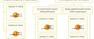
MOS transistors are divided into two types - with a built-in channel and with an induced channel. Each type has transistors with an N-channel and a P-channel.
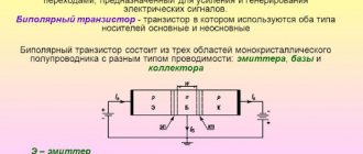
MOS transistor (MOSFET) device with an induced channel.
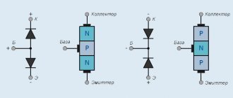
On the base (substrate) of a semiconductor with P-type electrical conductivity (for a transistor with an N-channel), two zones with increased N+-type electrical conductivity are created. All this is covered with a thin layer of dielectric, usually silicon dioxide SiO2. Metal leads from N+-type regions, called drain and source, pass through the dielectric layer. Above the dielectric is a metal gate layer. Sometimes a lead also comes from the substrate, which is short-circuited with the source
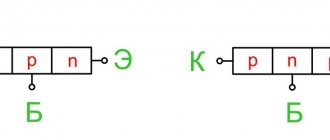
Scheme (structure)
In the diagram below you can see the approximate structure of a polar type transistor. Its leads are connected to the metallized sections of the gate, source and drain. The diagram depicts exactly a p-channel device, the gate of which is an n-layer. It has a much lower resistivity than the channel region of the p-layer. The np transition region is largely located in the p-layer.
Schematic representation of an electrotransistor with np channels
Operation of a MOS transistor (MOSFET) with an N-type induced channel.
Let's connect a voltage of any polarity between the drain and source. In this case, no electric current will flow, since between the N+ zones there is a region P that does not allow electrons to pass through. Further, if a positive voltage is applied to the gate relative to the source Uzi, an electric field will arise. It will push positive ions (holes) from the P zone towards the substrate. As a result, the concentration of holes under the gate will begin to decrease, and their place will be taken by electrons attracted by the positive voltage on the gate.
When Uzi reaches its threshold value, the electron concentration in the gate region will exceed the hole concentration. A thin channel with N-type electrical conductivity will be formed between the drain and the source, through which the current Ic will flow. The higher the voltage at the gate of the transistor Uzi, the wider the channel and, therefore, the greater the current. This mode of operation of a field-effect transistor is called enrichment mode.
The operating principle of an MOS transistor with a P-type channel is the same, only a negative voltage must be applied to the gate relative to the source.
Semiconductor Interaction
You and I know from the article Bipolar transistor that there are two types of artificial doped semiconductors. These are N-type semiconductor and P-type semiconductor. As you remember, in an N-type semiconductor we have an excess of electrons (there are a LOT of them):
And in a P-type semiconductor there is an excess of holes:
If you haven't forgotten, electrons have a negative charge (-), and holes have a positive charge (+). Therefore, in the pictures we filled our semiconductor bars with the corresponding charges.
What happens if you combine them with each other?
Since electrons and holes are constantly in chaotic motion, diffusion . What is diffusion? As Wikipedia tells us, diffusion is the process of mutual penetration of molecules or atoms of one substance between molecules or atoms of another substance. (more details in the article about the structure of the atom).
Example:
If you use a steam whisperer, then in this case your smelly molecules from the fart will mix with air molecules and the neighbor across the desk will smell your smell of dumplings that you ate for dinner.
The same thing happens at the semiconductor interface! Electrons and holes begin to mix.
But if your stinking molecules released from a fart can easily mix with the air until they occupy the entire space of the office, then there is a stumbling block at the border of the PN transition. And it lies in the fact that electrons and holes have a charge and begin to interact with each other. The rule begins to work: like charges repel, and unlike charges attract. Since electrons and holes have opposite charges, they begin to attract each other. That is, on one side there is diffusion, and on the other side there is interaction of charges. When all this settles down, you get this picture:
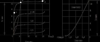
Current-voltage characteristics (CV characteristics) of a MOS transistor with an induced channel.
The current-voltage characteristics of a field-effect transistor with an insulated gate are similar to the current-voltage characteristics of a field-effect transistor with a control PN junction. As can be seen in graph a), initially the current Ic increases in direct proportion to the increase in voltage Uc. This area is called the ohmic region (Ohm's law applies), or the saturation region (the transistor channel is saturated with charge carriers). Then, when the channel expands almost to its maximum, the current Ic practically does not increase. This area is called the active region.
When Uc exceeds a certain threshold value (the breakdown voltage of the PN junction), the structure of the semiconductor is destroyed and the transistor turns into an ordinary conductor. This process cannot be restored, and the device becomes unusable.
Operation of an MOS transistor (MOSFET) with a built-in N-type channel.
Let's connect the voltage between the drain and source Ui of any polarity to the transistor. Let's leave the shutter disabled (Uzi = 0). As a result, a current Ici, which is a flow of electrons, will flow through the channel.
Next, we connect a negative voltage to the gate relative to the source. A transverse electric field will arise in the channel, which will begin to push electrons out of the channel zone towards the substrate. The number of electrons in the channel will decrease, its resistance will increase, and the current Ic will decrease. As the negative gate voltage increases, the current decreases. This state of operation of the transistor is called depletion mode.
If a positive voltage is applied to the gate, the resulting electric field will attract electrons from the drain, source, and substrate regions. The channel will expand, its conductivity will increase, and the current Ic will increase. The transistor will enter enrichment mode.
As we can see, a MOS transistor with a built-in channel is capable of operating in two modes - in depletion mode and in enrichment mode.
What are drain, source and gate
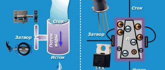
The field effect transistor has three terminals. The terminal from which electrons (majority carriers) begin their journey is called SOURCE. From the word "source". In colloquial speech, we call a spring from which clean water flows.
This is certainly not the 5th element, NOOO!!! Peltier element.
Therefore, it will not be difficult to remember that SOURCE is the output from where the main charge carriers begin their journey. In this case, these are electrons. The place where they flock is called DRAIN.
These two concepts will not be difficult to remember if you remember the drainage system from the roofs of your houses.
The source will be a pipe that collects all raindrops from slate or corrugated sheeting
And the drain will be the end of the pipe, from which all the rainwater will run out to the ground:
But again, don't forget that we're talking about electrons! And the electrons run to the plus. That is, in our language, it turns out that we apply a plus to the DRAIN, and a minus to the SOURCE.
What is the third output for?
So, just for fun, let’s cut off our drainpipe somewhere and stick this little gadget in there:
It's called a disc valve. What would we achieve if we stuck this butterfly valve into our drainpipe? Yes, by turning the steering wheel, we could regulate the flow of water! We can completely block the pipe, then in this case there is no need to wait for rainwater at the drain. Or we can open it halfway and regulate the flow of water from the drain so that when it rains, the flow of water does not wash away the beds and make a large hole in the ground. Comfortable? Comfortable.
Color marking of resistors is known from the calculator.
So, the third terminal of the field-effect transistor, which is connected to the P semiconductor, is also called a GATE and serves precisely to regulate the strength of the current in the bar through which the electric current flows. To do this, it is enough to apply voltage to it so that the PN junction is turned on in reverse direction, that is, in our case, apply a MINUS relative to the SOURCE. The whole picture will look something like this:
Advantages and disadvantages of field-effect transistors over bipolar ones.
Field-effect transistors have practically replaced bipolar transistors in a number of applications. They are most widely used in integrated circuits as keys (electronic switches)
The main advantages of field-effect transistors
- Due to the very high input resistance, the field-effect transistor circuit consumes extremely little energy, since it consumes virtually no input current.
- The current gain of field-effect transistors is much higher than that of bipolar transistors.
- The noise immunity and reliability of operation are significantly higher, since due to the absence of current through the gate of the transistor, the control circuit on the gate side is isolated from the output circuit on the drain and source sides.
- Field-effect transistors have an order of magnitude higher speed of transition between the states of conduction and non-conduction of current. Therefore, they can operate at higher frequencies than bipolar ones.
The main disadvantages of field-effect transistors
- FETs have a higher voltage drop due to the high resistance between drain and source when the device is in the on state.
- The structure of field-effect transistors begins to deteriorate at a lower temperature (150C) than the structure of bipolar transistors (200C).
- Despite the fact that field-effect transistors consume much less energy compared to bipolar transistors, when operating at high frequencies the situation changes dramatically. At frequencies higher than approximately 1.5 GHz, the power consumption of MOSFETs begins to increase exponentially. Therefore, the speed of processors stopped growing so rapidly, and their manufacturers switched to a “multi-core” strategy.
- When manufacturing high-power MOS transistors, a “parasitic” bipolar transistor appears in their structure. In order to neutralize its influence, the substrate is short-circuited with the source. This is equivalent to shorting the base and emitter of the parasitic transistor. As a result, the voltage between the base and emitter of the bipolar transistor will never reach the voltage required for it to open (about 0.6V is required for the PN junction inside the device to begin conducting).
However, if there is a rapid voltage jump between the drain and source of the field-effect transistor, the parasitic transistor may accidentally open, as a result of which the entire circuit may fail.
- The most important disadvantage of field-effect transistors is their sensitivity to static electricity. Since the insulating dielectric layer on the gate is extremely thin, sometimes even a relatively low voltage is enough to destroy it. And discharges of static electricity, present in almost every environment, can reach several thousand volts.
Therefore, they try to create the external housings of field-effect transistors in such a way as to minimize the possibility of unwanted voltage occurring between the electrodes of the device. One such method is to short-circuit the source with the substrate and ground them. Also, some models use a specially built-in diode between the drain and source. When working with integrated circuits (chips) consisting primarily of field-effect transistors, it is advisable to use grounded antistatic wrist straps. When transporting integrated circuits, vacuum antistatic packaging is used
What is it needed for
PTs are needed to control the output current using the generated electric field and change its most important parameters. Structures based on field-effect transistors are often used in digital and analog integrated circuits.
n- and p-channel electrotransistors
It is through field control that these transistors influence the magnitude of the voltage applied to their gate. This distinguishes them from bipolar transistors, which are controlled by the current that flows through their base. PTs consume significantly less electricity, which determines their popularity when used in waiting and tracking devices, as well as low-consumption integrated circuits (when organizing sleep mode).
You may be interested in Features of calculating a voltage divider
Important! Some of the most famous devices based on the action of field-effect transistors are TV remote controls and electronic wristwatches. Due to their design and the use of DC, these devices can operate for years from one tiny power source in the form of a battery.
Schematic view of a field-effect transistor