Transistor switch
With the development of electronic pulse technology, a transistor switch in one form or another is used in almost any electronic device. Moreover, most microcircuits consist of tens, hundreds and millions of transistor switches. And digital technology cannot do without them at all. In general, the modern world of electronics is unthinkable without the device discussed in this article.
Here we will learn how to calculate a transistor switch using a bipolar transistor (BT). One of their common uses is matching a microcontroller with a relatively powerful load: powerful LEDs, seven-segment indicators, stepper motors, etc.
The main task of any transistor switch is to switch a powerful load at the command of a low-power signal.
Electronic keys have deeply penetrated and taken root in the field of automation, displacing mechanical electromagnetic relays. Unlike an electromagnetic relay, a transistor switch is devoid of moving mechanical elements, which significantly increases the service life, performance and reliability of the device. The speed of switching on and off, that is, the frequency of operation, is incomparably higher than that of a relay.
However, electromagnetic relays also have useful properties. The voltage drop across closed relay contacts is significantly less than across semiconductor elements in the open state. In addition, the relay has galvanic isolation of high-voltage circuits from low-voltage ones.
How does a transistor switch work?
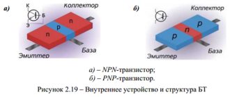
In this article we will look at how a transistor switch on a bipolar transistor works. Such semiconductor elements are produced in two types - npn and pnp structures, which differ in the type of semiconductor used (in a p-semiconductor, positive charges - “holes" - predominate; in an n-semiconductor, negative charges - electrons).
The BT terminals are called base, collector and emitter, which have a graphical designation on electrical circuit drawings, as shown in the figure.
In order to understand the operating principle and individual processes occurring in bipolar transistors, they are depicted as two diodes connected in series and back-to-back.
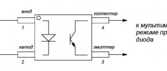
The most common diagram of a BT operating in key mode is shown below.
To open a transistor switch, you need to apply potentials of a certain sign to both pn junctions. The collector-base junction must be reverse biased, and the base-emitter junction must be forward biased. To do this, the electrodes of the power supply UKE are connected to the terminals of the base and collector through a load resistor RK . Please note that the positive potential UKE via RK , and the negative potential is supplied to the emitter. For a semiconductor pnp structure, the polarity of connecting the power supply UKE is reversed.
The resistor in the collector circuit RK serves as a load, which simultaneously protects the bipolar transistor from short circuit.
The command to open the BT is supplied by the control voltage UBE , which is supplied to the base and emitter terminals through a current-limiting resistor RB . The value of UBE must be at least 0.6 V, otherwise the emitter junction will not open completely, which will cause additional energy losses in the semiconductor element.
In order not to confuse the polarity of connecting the supply voltage UKE and the control signal UBE BT of different semiconductor structures, pay attention to the direction of the emitter arrow. The arrow points in the direction of the flow of electric current. Focusing on the direction of the arrow, it is enough to simply position the voltage sources in the correct way.
Input static characteristic
A bipolar transistor can operate in two fundamentally different modes - amplifier mode and switch mode. The operation of BT in amplification mode has already been discussed in detail with examples of calculations in several articles. I highly recommend checking them out. The key operating mode of the BT is discussed in this article.
Like an electric switch, a transistor switch can (and should) be in only one of two states - on (open) and off (closed), which is displayed in sections of the load straight line located on the input static characteristic of the bipolar transistor. In section 3-4 , the BT is closed, and at its terminals there are UKE . The collector current IK is close to zero. At the same time, there is also no current in the IK base circuit, which is actually why the BT is closed. The area on the input static characteristic corresponding to the closed state is called cutoff area .
The second state is that the BT is completely open, which is shown in section 1-2 . As can be seen from the characteristics, the current IK has a certain value, which depends on the values of UKE and RK . IB also flows in the base-emitter circuit , the magnitude of which is sufficient to completely open the bipolar transistor.
The voltage drop across the collector-emitter pn junction, depending on the series of the transistor and its power, ranges from hundredths to tenths of a volt. Such a working area of the BT, in which it is completely open, is called saturation area .
In the third region, the semiconductor switch occupies an intermediate position between open and closed, that is, it is slightly open or slightly closed. Such a region used for a transistor operating as an amplifier is called active region .
Transistor switch calculation
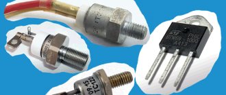
We will calculate the transistor switch on a bipolar transistor using the example of connecting an LED to a 9 V power source, that is, to the crown. An ordinary 1.5 V battery is suitable as a control signal. For example, take the BT npn structure of the 2222A series. Although any other will do, for example 2N2222, PN2222, BC547 or Soviet MP111B, etc.
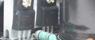
The transistor switch circuit under consideration is quite simple to assemble on a breadboard and make the appropriate measurements using a multimeter, thereby assessing the accuracy of our calculations.
Further, all calculations come down to determining the resistances of the collector resistor RK and base RB . Although it is more logical, especially when connecting a powerful load, to first select the transistor based on current and voltage, and then calculate the parameters of the resistors. However, in our and most other cases, the load current is relatively small and U of the power source is low, so almost any low-power BT is suitable.
All source data are summarized in a table.
Calculation procedure
We begin the calculation by determining the resistance of the resistor RK , which is designed to limit the amount of current IK flowing through the LED VD. RK is found according to Ohm's law:
The value of IK is equal to IVD = 0.01 A. Let’s find the voltage drop across the resistor:
the value of UKE , it is equal to 9 V, ΔUVD is also known and is equal to 2 V. And the voltage drop at the collector-emitter junction for most modern low-power BTs is up to 0.1 V. Therefore, we will accept with a margin ΔUKE = 0.1 V. Now Let's substitute all the values into the above formula:
Find the resistance RK :
The closest standard resistor values are 680 ohms and 750 ohms. We choose a resistor of a larger value RК = 750 Ohm. In this case, the current flowing through the IVD in the collector circuit will decrease slightly. Let's recalculate its value:
Now it remains to determine the resistance of the resistor in the base circuit RB :
The formula contains two unknowns at once - ΔURb and IB . Let's first find the voltage drop across the resistor ΔURb :
UBE - 1.5 V. And the voltage drop at the base-emitter junction is on average 0.6 V, hence:
To determine the base current IB, it is necessary to know I K , which we previously recalculated (IK = 0.0092 A), and the current gain of the bipolar transistor, denoted by the letter β (beta). β coefficient is always given in reference books or datasheets, but it is much more convenient and accurate to determine it using a multimeter. The 2222A we use has β = 231 units.
From the table of standard resistor values, select the nearest lower value (to guarantee the opening of the BT) 22 kOhm.
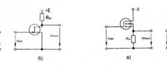
For a more accurate selection of parameters, instead of constant resistors in the circuit, include variable resistors connected according to the diagram below.
Thus, we performed the calculation of the transistor switch, that is, we determined RC and RB based on the given initial data. A more complete calculation includes determining the power dissipation of the indicated resistors, but due to the insignificant load in our example, resistors with minimal power dissipation are suitable.
More articles on this topic
- Replacing the electrolytic capacitor
- Characteristics of capacitors
- Capacitive voltage divider
- What is PWM - Pulse Width Modulation?
NPN transistor operation:
Now that the n side of the diode has the most electrons and the p side has the most holes, all voltage connections are arranged as forward and reverse bias respectively. The emitter base junction is configured as reverse bias and the collector base junction is configured as forward bias. The depletion region of this emitter-base region is narrower compared to the depletion region at the collector-base intersection.
Since the junction is reverse biased (emitter), the holes flow from the power supply to the N junction. The electron then moves towards p. Here some electron is neutralized. The remaining electrons move towards n. The voltage drop relative to the emitter and base is VBE as the input side.
In N-type emitters, the charge carriers are mainly electrons. Consequently, electrons are transferred through the N-type emitters to the P-type base. The current will flow through the emitter-base or EB junction. This current is known as emitter current (Ie). Here, the emitter current (IE) flows from the output side and flows in two directions; one is IB and the other is IC. So we can write:
It will be interesting➡ What is meant by touch tension?
IE=IB+IC
However, the base region is relatively thin and lightly doped. Consequently, most of the electrons pass through the base region and only a few of them recombine with the available holes. The base current is minimal compared to the emitter current. Typically this is up to 5% of the total emitter current.
The current flowing from the rest of the electrons is called collector current (IC). YC is relatively high compared to baseline (IB).