What is an electronic key?
A key is, to simplify it, an ordinary switch. With its help, the electrical circuit is closed and opened. A bipolar transistor has three terminals:
- Collector.
- Emitter.
- Base.
Electronic switches are built on bipolar semiconductors - the design is simple and does not require a large number of elements. The switch is used to close and open a section of the circuit. This happens with the help of a control signal (which is generated by the microcontroller) supplied to the base of the transistor.
Advantages and disadvantages of bipolar transistors
The advantages of bipolar transistors in comparison with analogues include:
- control of electrical charges;
- reliability in operation;
- resistance to frequency interference;
- low noise characteristics;
The disadvantages include:
- has a low input resistance, due to which the signal amplification characteristics deteriorate;
- severe sensitivity to static charges;
- the connection diagram assumes the presence of 2 power supplies;
- At high temperatures the transistor may be damaged.
Load switching
Using simple circuits on transistor switches, you can switch currents in the range of 0.15... 14 A, voltages 50... 500 V. It all depends on the specific type of transistor. The key can switch a load of 5-7 kW using a control signal whose power does not exceed hundreds of milliwatts.
Instead of transistor switches, simple electromagnetic relays can be used. They have the advantage that they do not heat up during operation. But the frequency of on and off cycles is limited, so they cannot be used in inverters or switching power supplies to create a sine wave. But in general, the principle of operation of a switch on a semiconductor transistor and an electromagnetic relay is the same.
Electromagnetic relay
A relay is an electromagnet that controls a group of contacts. An analogy can be drawn with a conventional push-button switch. Only in the case of a relay, the force is taken not from the hand, but from the magnetic field that is located around the excitation coil. The contacts can switch a very large load - it all depends on the type of electromagnetic relay. These devices have become very widespread in automotive technology - with their help, all powerful consumers of electricity are turned on.
This allows you to divide all the electrical equipment of the car into a power part and a control part. The current consumption of the relay excitation winding is very small. And the power contacts are coated with precious or semi-precious metals, which eliminates the possibility of an arc. Transistor switch circuits for 12 volts can be used instead of relays. At the same time, the functionality of the device improves - the switching on is silent, the contacts do not click.
Electromagnetic relay terminals
Typically, electromagnetic relays have 5 terminals:
- Two contacts for control. The excitation winding is connected to them.
- Three contacts intended for switching. One common contact that is normally closed and normally open with the others.
Depending on which switching scheme is used, groups of contacts are used. The field-effect transistor switch has 3-4 contacts, but it functions in approximately the same way.
How does an electromagnetic relay work?
The operating principle of an electromagnetic relay is quite simple:
- The winding is connected to the power supply through a button.
- The power contacts of the relay are connected to the consumer's power supply circuit break.
- When you press the button, power is supplied to the winding, the plate is attracted and the group of contacts is closed.
- Current is supplied to the consumer.
Transistor switches work in approximately the same way - only a group of contacts is missing. Their functions are performed by a semiconductor crystal.
Transistor conductivity
One of the operating modes of the transistor is key. Essentially, it acts as a switch. There is no point in touching on the circuits of the amplifier stages; they do not relate to this mode of operation. Semiconductor triodes are used in all types of devices - in automotive technology, in everyday life, in industry. All bipolar transistors can have this type of conductivity:
- PNP.
- NPN.
The first type includes semiconductors made on the basis of germanium. These elements became widespread more than half a century ago. A little later, silicon, which has reverse conductivity - npn, began to be used as an active element.
The operating principle of the devices is the same; they differ only in the polarity of the supply voltage, as well as in certain parameters. Silicon semiconductors are currently more popular; they have almost completely replaced germanium semiconductors. And most devices, including transistor switches, are made on bipolar silicon elements with npn conductivity.
Device design
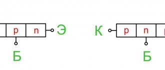
The design circuit of a PNP-type transistor consists of two regions of p-type semiconductor material on either side of a region of n-type material, as shown in the figure below.
The arrow identifies the emitter and the generally accepted direction of its current (“inward” for a PNP transistor).
The PNP transistor has very similar characteristics to its NPN bipolar counterpart, except that the directions of currents and voltage polarities in it are reversed for any of the possible three connection schemes: common base, common emitter and common collector.
PNP transistor designation
PNP transistor symbol Where, E = emitter, B = base, C = collector
The middle level (N-type) is called the B-Base terminal. The left side P-type layer acts as the E-Emitter pin and the right side P-type layer known as the C-Collector pin. PNP transistor
When forming an NPN transistor, one P-type semiconductor material is placed between two N-type semiconductors, as described in the article (Link NPN Transistor). While in a PNP transistor, one N-type semiconductor is placed between two P-type semiconductor materials.
The PNP transistor uses two types of diodes. These are PN and NP diodes, respectively. These PN junction diodes are called collector-base junction or CB junction and base-emitter junction or BE junction.
In a P-type semiconductor material, the charge carriers are primarily holes. Thus, in this transistor, current generation occurs only due to the movement of the holes.
The emitter and collector (P-type) regions are comparatively more doped than the N-type base. The Emitter and Collector regions are wider compared to the base.
Typically, an N-type semiconductor has more free electrons available. But the width of the middle layer in this case is narrower and slightly alloyed. Connecting a transistor, image credit – S. Blank, PNP transistor, CC BY-SA 4.0
Transistor in switch mode
A transistor in switch mode performs the same functions as an electromagnetic relay or switch. The control current flows as follows:
- From the microcontroller via the base-emitter junction.
- In this case, the collector-emitter channel opens.
- Through the collector-emitter channel you can pass a current whose value is hundreds of times greater than the base one.
The peculiarity of transistor switches is that the switching frequency is much higher than that of a relay. A semiconductor crystal is capable of making thousands of transitions from an open state to a closed state and back in one second. Thus, the switching speed of the simplest bipolar transistors is about 1 million times per second. For this reason, transistors are used in inverters to create a sine wave.
Types of bipolar transistors
Bipolar transistors are classified into the following types: 1. Based on the source material - germanium or silicon. 2. According to production technology - alloy, epitaxial-planar, conversion, etc. 3. According to the mechanism of movement of charge carriers - drift and diffusion. 4. By power dissipation - low power (up to 0.3 W), medium power (from 0.3 to 3 W) and high power (more than 3 W). 5. According to the range of operating frequencies - low frequency (up to 3 MHz), medium (from 3 to 30 MHz), high (from 30 to 300 MHz), ultra-high frequency (more than 300 MHz).
Transistor operating principle
The element works exactly the same as in power amplifier mode. Essentially, a small control current is applied to the input, which is amplified several hundred times due to the fact that the resistance between the emitter and collector changes. Moreover, this resistance depends on the amount of current flowing between the emitter and the base.
Depending on the type of transistor, the pinout changes. Therefore, if you need to determine the pins of an element, you need to consult a reference book or datasheet. If it is not possible to refer to the literature, you can use reference books to determine conclusions. There is also a peculiarity of transistors - they may not open completely. Relays, for example, can be in two states - closed and open. But for a transistor, the resistance of the emitter-collector channel can vary within wide limits.
Measuring the current gain of a bipolar transistor
If the tester has the ability to measure the current transfer coefficient, then you can check the operation of the transistor by installing the transistor leads into the corresponding sockets.
We recommend reading: Varistor: principle of operation, main characteristics, designation on the diagram
Current transfer coefficient is the ratio of the collector current to the base current.
The higher the gain, the more collector current can be controlled by the base current, all other things being equal.
The pinout (pin name) and other data can be taken from the data sheets (reference data) for the corresponding transistor. Data sheets can be found on the Internet through search engines.
The tester will show on the display the current transfer (gain) coefficient, which must be compared with the reference data.
The current transfer coefficient of low-power transistors can reach several hundred.
For powerful transistors it is significantly smaller - several units or tens.
However, there are powerful transistors with a transfer coefficient of several hundred or thousand. These are the so-called Darlington pairs.
A Darlington pair consists of two transistors. The output current of the first transistor is the input current for the second.
The overall current transfer coefficient is the product of the coefficients of the first and second transistors.
The Darlington pair is made in a common housing, but it can also be made from two separate transistors.
An example of transistor operation in switch mode
Gain is one of the main characteristics of a transistor. It is this parameter that shows how many times the current flowing through the emitter-collector channel is higher than the base one. Let's say the coefficient is 100 (this parameter is designated h21E). This means that if a current of 1 mA (base current) is supplied to the control circuit, then at the collector-emitter junction it will be 100 mA. Consequently, the incoming current (signal) was amplified.
During operation, the transistor heats up, so it needs passive or active cooling - radiators and coolers. But heating occurs only when the collector-emitter passage does not open completely. In this case, a lot of power is dissipated - it needs to be put somewhere, you have to “sacrifice” the efficiency and release it in the form of heat. Heating will be minimal only in cases where the transistor is closed or fully open.
Bipolar transistor device
According to standard circuits, the letter “B” is called “Base” - the inner layer of the device, its foundation, which leads to the conversion or change of the current signal. The arrow in the circle shows the movement of current charges in “E”.
“E” - “Emitter” - the internal main component of the transistor, designed to transfer charged elementary particles to “B”.
“K” - “Collector” is the second component of the transistor device, which collects the same charges that pass through “B”.
The “Base” layer is structurally very thin due to the recombination of charged particles that go through the base layer with the constituent particles of this layer. At the same time, the “Collector” layer is designed as wide as possible for high-quality collection of charges.
Saturation mode
All transistors have a certain input current threshold. Once this value is reached, the gain ceases to play a big role. In this case, the output current does not change at all. The voltage at the base-emitter contacts can be higher than between the collector and emitter. This is a saturation state, the transistor opens completely. The key mode means that the transistor operates in two modes - either it is completely open or closed. When the control current supply is completely cut off, the transistor closes and stops passing current.
Transistor switch
With the development of electronic pulse technology, a transistor switch in one form or another is used in almost any electronic device. Moreover, most microcircuits consist of tens, hundreds and millions of transistor switches. And digital technology cannot do without them at all. In general, the modern world of electronics is unthinkable without the device discussed in this article.
Here we will learn how to calculate a transistor switch using a bipolar transistor (BT). One of their common uses is matching a microcontroller with a relatively powerful load: powerful LEDs, seven-segment indicators, stepper motors, etc.
The main task of any transistor switch is to switch a powerful load at the command of a low-power signal.
Electronic keys have deeply penetrated and taken root in the field of automation, displacing mechanical electromagnetic relays. Unlike an electromagnetic relay, a transistor switch is devoid of moving mechanical elements, which significantly increases the service life, performance and reliability of the device. The speed of switching on and off, that is, the frequency of operation, is incomparably higher than that of a relay.
However, electromagnetic relays also have useful properties. The voltage drop across closed relay contacts is significantly less than across semiconductor elements in the open state. In addition, the relay has galvanic isolation of high-voltage circuits from low-voltage ones.
How does a transistor switch work?
In this article we will look at how a transistor switch on a bipolar transistor works. Such semiconductor elements are produced in two types - npn and pnp structures, which differ in the type of semiconductor used (in a p-semiconductor, positive charges - “holes" - predominate; in an n-semiconductor, negative charges - electrons).
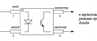
The BT terminals are called base, collector and emitter, which have a graphical designation on electrical circuit drawings, as shown in the figure.
In order to understand the operating principle and individual processes occurring in bipolar transistors, they are depicted as two diodes connected in series and back-to-back.
The most common diagram of a BT operating in key mode is shown below.
To open a transistor switch, you need to apply potentials of a certain sign to both pn junctions. The collector-base junction must be reverse biased, and the base-emitter junction must be forward biased. To do this, the electrodes of the power supply UKE are connected to the terminals of the base and collector through a load resistor RK . Please note that the positive potential UKE via RK , and the negative potential is supplied to the emitter. For a semiconductor pnp structure, the polarity of connecting the power supply UKE is reversed.
The resistor in the collector circuit RK serves as a load, which simultaneously protects the bipolar transistor from short circuit.
The command to open the BT is supplied by the control voltage UBE , which is supplied to the base and emitter terminals through a current-limiting resistor RB . The value of UBE must be at least 0.6 V, otherwise the emitter junction will not open completely, which will cause additional energy losses in the semiconductor element.
In order not to confuse the polarity of connecting the supply voltage UKE and the control signal UBE BT of different semiconductor structures, pay attention to the direction of the emitter arrow. The arrow points in the direction of the flow of electric current. Focusing on the direction of the arrow, it is enough to simply position the voltage sources in the correct way.
Input static characteristic
A bipolar transistor can operate in two fundamentally different modes - amplifier mode and switch mode. The operation of BT in amplification mode has already been discussed in detail with examples of calculations in several articles. I highly recommend checking them out. The key operating mode of the BT is discussed in this article.
Like an electric switch, a transistor switch can (and should) be in only one of two states - on (open) and off (closed), which is displayed in sections of the load straight line located on the input static characteristic of the bipolar transistor. In section 3-4 , the BT is closed, and at its terminals there are UKE . The collector current IK is close to zero. At the same time, there is also no current in the IK base circuit, which is actually why the BT is closed. The area on the input static characteristic corresponding to the closed state is called cutoff area .
The second state is that the BT is completely open, which is shown in section 1-2 . As can be seen from the characteristics, the current IK has a certain value, which depends on the values of UKE and RK . IB also flows in the base-emitter circuit , the magnitude of which is sufficient to completely open the bipolar transistor.
The voltage drop across the collector-emitter pn junction, depending on the series of the transistor and its power, ranges from hundredths to tenths of a volt. Such a working area of the BT, in which it is completely open, is called saturation area .
In the third region, the semiconductor switch occupies an intermediate position between open and closed, that is, it is slightly open or slightly closed. Such a region used for a transistor operating as an amplifier is called active region .
Transistor switch calculation
We will calculate the transistor switch on a bipolar transistor using the example of connecting an LED to a 9 V power source, that is, to the crown. An ordinary 1.5 V battery is suitable as a control signal. For example, take the BT npn structure of the 2222A series. Although any other will do, for example 2N2222, PN2222, BC547 or Soviet MP111B, etc.
The transistor switch circuit under consideration is quite simple to assemble on a breadboard and make the appropriate measurements using a multimeter, thereby assessing the accuracy of our calculations.
Further, all calculations come down to determining the resistances of the collector resistor RK and base RB . Although it is more logical, especially when connecting a powerful load, to first select the transistor based on current and voltage, and then calculate the parameters of the resistors. However, in our and most other cases, the load current is relatively small and U of the power source is low, so almost any low-power BT is suitable.
All source data are summarized in a table.
Calculation procedure
We begin the calculation by determining the resistance of the resistor RK , which is designed to limit the amount of current IK flowing through the LED VD. RK is found according to Ohm's law:
The value of IK is equal to IVD = 0.01 A. Let’s find the voltage drop across the resistor:
the value of UKE , it is equal to 9 V, ΔUVD is also known and is equal to 2 V. And the voltage drop at the collector-emitter junction for most modern low-power BTs is up to 0.1 V. Therefore, we will accept with a margin ΔUKE = 0.1 V. Now Let's substitute all the values into the above formula:
Find the resistance RK :
The closest standard resistor values are 680 ohms and 750 ohms. We choose a resistor of a larger value RК = 750 Ohm. In this case, the current flowing through the IVD in the collector circuit will decrease slightly. Let's recalculate its value:
Now it remains to determine the resistance of the resistor in the base circuit RB :
The formula contains two unknowns at once - ΔURb and IB . Let's first find the voltage drop across the resistor ΔURb :
UBE - 1.5 V. And the voltage drop at the base-emitter junction is on average 0.6 V, hence:
To determine the base current IB, it is necessary to know I K , which we previously recalculated (IK = 0.0092 A), and the current gain of the bipolar transistor, denoted by the letter β (beta). β coefficient is always given in reference books or datasheets, but it is much more convenient and accurate to determine it using a multimeter. The 2222A we use has β = 231 units.
From the table of standard resistor values, select the nearest lower value (to guarantee the opening of the BT) 22 kOhm.
For a more accurate selection of parameters, instead of constant resistors in the circuit, include variable resistors connected according to the diagram below.
Thus, we performed the calculation of the transistor switch, that is, we determined RC and RB based on the given initial data. A more complete calculation includes determining the power dissipation of the indicated resistors, but due to the insignificant load in our example, resistors with minimal power dissipation are suitable.
More articles on this topic
- Replacing the electrolytic capacitor
- Characteristics of capacitors
- Capacitive voltage divider
- What is PWM - Pulse Width Modulation?
Practical designs
There are a lot of practical schemes for using transistors in switch mode. They are often used to turn LEDs on and off to create special effects. The operating principle of transistor switches allows not only to make “toys”, but also to implement complex control circuits. But in designs it is imperative to use resistors to limit the current (they are installed between the source of the control signal and the base of the transistor). But the source of the signal can be anything - a sensor, a push-button switch, a microcontroller, etc.
3.1. Residual parameters of a closed transistor
a) When the value of the blocking voltage at the emitter junction changes, that is, when the cutoff depth () changes, the base current does not change and remains equal. This equality is called the current cutoff criterion.
b) Both in the deep cutoff mode and at the cutoff boundary, the emitter current is .
The equivalent circuit of the key in cut-off mode can be represented as:
| Rice. 2.1.a: Equivalent circuit of a key in cut-off mode |
Switch output voltage
c) From the diagram it is clear that the voltage applied to the emitter, control junction depends on the residual base current;
.
In its turn .
To maintain the cutoff mode when changing from and resistances, it is necessary to fulfill the following condition:
.
Otherwise, despite the negative polarity of the control signal, the transistor will switch to active mode.
d) In transistor switches, it is necessary to use transistors with low reverse transition currents.
Note:
Integrated circuits do not use negative control signals to turn off transistors because digital circuits are single-supply powered. The open state of the key does not correspond to the cut-off mode, but to the active mode at low collector current. This has a beneficial effect on reducing the duration of transient processes.
|
The transistor turn-off threshold is a conditional value. The more open, the more can be selected. Usually accepted.
Working with microcontrollers
When calculating a transistor switch, you need to take into account all the operating features of the element. In order for the control system on the microcontroller to work, amplification stages on transistors are used. The problem is that the output signal from the controller is very weak, it is not enough to turn on the power to the winding of the electromagnetic relay (or open the transition of a very powerful power switch). It is better to use a bipolar transistor switch to control the MOSFET element.
Simple designs are used, consisting of the following elements:
- Bipolar transistor.
- Resistor to limit input current.
- Semiconductor diode.
- Electromagnetic relay.
- Power supply 12 volts.
The diode is installed in parallel with the relay winding; it is necessary in order to prevent breakdown of the transistor by a pulse with a high EMF, which appears when the winding is turned off.
The control signal is generated by the microcontroller, goes to the base of the transistor and is amplified. In this case, power is supplied to the winding of the electromagnetic relay - the collector-emitter channel opens. When the power contacts are closed, the load is turned on. The transistor switch is controlled in a fully automatic mode - practically no human intervention is required. The main thing is to correctly program the microcontroller and connect sensors, buttons, and actuators to it.
Step-by-step instructions for checking with a multimeter
Before starting the test, first of all, the structure of the triode device is determined, which is indicated by the emitter junction arrow. When the direction of the arrow points towards the base, then this is the PNP variant, the direction opposite to the base indicates NPN conductivity.
Testing a PNP transistor with a multimeter consists of the following sequential operations:
- We check the reverse resistance; to do this, we connect the “positive” probe of the device to its base.
- The emitter junction is tested; for this we connect the “negative” probe to the emitter.
- To check the collector, move the negative probe onto it.
The results of these measurements should show a resistance within the value of “1”.
To check direct resistance, swap the probes:
- We attach the “negative” probe of the device to the base.
- We alternately move the “positive” probe from the emitter to the collector.
- On the multimeter screen, the resistance readings should be from 500 to 1200 Ohms.
These readings indicate that the transitions are not broken, the transistor is technically sound.
Many amateurs have difficulty identifying the base, and, accordingly, the collector or emitter. Some advise starting to determine the base, regardless of the type of structure, in this way: alternately connecting the black probe of the multimeter to the first electrode, and the red probe alternately to the second and third.
The base will be detected when the voltage across the device begins to drop. This means that one of the transistor pairs has been found - “base-emitter” or “base-collector”. Next, you need to determine the location of the second pair in the same way. The common electrode of these pairs will be the base.
It will be interesting➡ What is a load switch and how is it used?
Verification methods
Any repair of electronics and electrical equipment begins with an external inspection, and then proceeds to measurements. This approach allows you to localize most faults. To find a varistor on the board, look at the figure below - this is what varistors look like. Sometimes they can be confused with capacitors, but can be distinguished by their markings.
If the element is burnt out and the markings cannot be read, look at this information on the device diagram. On the board and in the diagram it can be designated by the letters RU. The conventional graphic symbol looks like this.
There are three ways to test a varistor quickly and easily:
- Visual inspection.
- Call. This can be done with a multimeter or any other device that has a continuity test function.
- Resistance measurement. This can be done with a high-range ohmmeter, multimeter or megger.
A varistor fails when a large or prolonged current passes through it. Then the energy is dissipated in the form of heat, and if its amount is greater than that determined by the design, the element burns out. The housing of these components is made of a hard dielectric material, such as ceramic or epoxy coating. Therefore, when it fails, the integrity of the outer coating is most often damaged.
You can visually check the varistor for functionality - there should be no cracks on it, as in the photo:
The next method is to check the varistor with a tester in continuity mode. This cannot be done in the circuit, because the dialing can work through parallel-connected elements. Therefore, you need to unsolder at least one of its legs from the board.
Important: you should not check the elements for serviceability without desoldering them from the board - this may give false readings from the measuring instruments. Since in the normal state (without voltage applied to the terminals) the resistance of the varistor is high, it should not ring through. The test is performed in both directions, that is, by swapping the multimeter probes twice
The test is performed in both directions, that is, by swapping the multimeter probes twice
Since in the normal state (without voltage applied to the terminals) the resistance of the varistor is high, it should not ring through. The test is performed in both directions, that is, by swapping the multimeter probes twice.
On most multimeters, the continuity mode is combined with the diode testing mode. It can be found by the diode icon on the mode selector scale. If there is a sound indication sign next to it, it probably also has a dial tone.
Another way to test a varistor for breakdown with a multimeter is to measure the resistance. You need to set the device to the maximum measurement limit, in most devices this is 2 MOhms (megaohms, designated as 2M or 2000K). The resistance must be equal to infinity. In practice, it can be lower, within 1-2 MOhm.
Interesting! The same can be done with a megaohmmeter, but not everyone has one. It is worth noting that the voltage at the megohmmeter terminals should not exceed the classification voltage of the component being tested.
This ends the available methods for checking a varistor. This time, the multimeter will help the radio amateur find the faulty element, as in a large number of other cases. Although in practice a multimeter is not always needed in this matter, because the matter rarely goes beyond a visual inspection. Replace the burnt element with a new one, designed for voltage and with a diameter no less than the burnt one, otherwise it will burn out even faster than the previous one.
Use of transistors in designs
You need to study all the requirements for semiconductors that you are going to use in the design. If you plan to control the winding of an electromagnetic relay, then you need to pay attention to its power. If it is high, then it is unlikely to be possible to use miniature transistors like KT315: they will not be able to provide the current necessary to power the winding. Therefore, it is recommended to use high-power field-effect transistors or assemblies in power engineering. Their input current is very small, but the gain is large.
You should not use powerful relays to switch weak loads: this is unreasonable. Be sure to use high-quality power sources, try to choose the voltage so that the relay operates in normal mode. If the voltage is too low, the contacts will not attract and switching will not occur: the magnitude of the magnetic field will be small. But if you use a source with a high voltage, the winding will begin to heat up and may even fail.
Be sure to use low and medium power transistors as buffers when working with microcontrollers if you need to turn on powerful loads. It is better to use MOSFET elements as power devices. The connection diagram to the microcontroller is the same as that of the bipolar element, but there are slight differences. The operation of a transistor switch using MOSFET transistors occurs in the same way as with bipolar ones: the transition resistance can change smoothly, transferring the element from an open state to a closed state and back.
Bipolar transistor connection circuits
A bipolar transistor has three terminals: emitter, collector and base. A signal comes to two of them, and from the other two it is removed, because one of them is common for entry and exit. So, which electrode is connected to the common bus, so is the connection diagram: with a common emitter (CE), a common base (CB) or a common collector (CC).
a) The connection circuit for a bipolar transistor with an OE is used most often in practice. In the above circuit, the input signal is supplied between the base and emitter through a decoupling capacitor Cp in order to cut off the DC voltage from the previous stage and not affect the power supply to the next stage. The amplified alternating voltage is removed from the collector and common terminal. This connection circuit provides both current and voltage gain. Such a connection will have a high output resistance (up to tens of kiloohms and depends on the value of Rk), but a low input resistance (500-1000 Ohms).
b) The following diagram shows switching on with OK. The bipolar transistor in this case works as a current amplifier and the voltage values at the input and output are almost the same. A feature of this connection is the high input resistance (from 10 kOhm to 500 kOhm), which provides good matching with the signal source stage. Also, the phase of the output voltage coincides with the phase of the input (there is no “flip” of the output signal, as in a circuit with an OE). Therefore, such a connection is called an emitter follower. But its output resistance is low, which greatly depends on the load resistance Re.
c) In the circuit with OB, we “ground” the base to the common wire through the capacitor Sat. In this case, the transistor only amplifies voltage, but there is no current amplification. Its input resistance is small (tens of ohms), and such a connection is used mainly in generators.
Connection diagram with a common base.
This circuit is very good when using high frequency signals. In principle, this is what switching on the transistor is used for in the first place. Very big disadvantages are the low input resistance and, of course, the lack of current amplification. See for yourself, at the input we have the emitter current I_e, at the output I_k.
I_e = I_k + I_b
That is, the emitter current is greater than the collector current by a small amount of the base current. This means that there is not just no current gain, moreover, the output current is slightly less than the input current. Although, on the other hand, this circuit has a fairly large voltage transfer coefficient. These are the advantages and disadvantages, let’s continue...
Connection diagram for a bipolar transistor with a common collector
This is what the wiring diagram for a bipolar transistor with a common collector looks like. Doesn't remind you of anything? If we look at the circuit from a slightly different angle, we will recognize our old friend here - the emitter follower. There was almost a whole article about it (here it is), so we have already covered everything related to this scheme. Meanwhile, we are waiting for the most commonly used circuit - with a common emitter.
Connection circuit for a bipolar transistor with a common emitter.
This circuit has earned popularity for its amplifying properties. Of all the circuits, it gives the greatest gain in current and voltage; accordingly, the increase in signal power is also large. The disadvantage of the circuit is that the amplification properties are strongly influenced by increasing temperature and signal frequency.
We got acquainted with all the circuits, now let’s take a closer look at the last (but not the least important) amplifier circuit based on a bipolar transistor (with a common emitter). First, let's depict it a little differently:
There is one minus here - the grounded emitter. When the transistor is turned on in this way, there are nonlinear distortions at the output, which, of course, must be combated. Nonlinearity occurs due to the influence of the input voltage on the emitter-base junction voltage. Indeed, there is nothing “extra” in the emitter circuit; the entire input voltage turns out to be applied precisely to the base-emitter junction. To cope with this phenomenon, we add a resistor to the emitter circuit. So we will receive negative feedback.
We recommend reading: LM358 microcircuit: datasheet in Russian, application, analogues, pin assignments
What is this?
In short, the principle of negative feedback is that some part of the output voltage is transferred to the input and subtracted from the input signal. Naturally, this leads to a decrease in the gain, since the input of the transistor, due to the influence of feedback, will receive a lower voltage value than in the absence of feedback.
Nevertheless, negative feedback is very useful for us. Let's see how it will help reduce the influence of the input voltage on the voltage between the base and emitter.
So, even if there is no feedback, an increase in the input signal by 0.5 V leads to the same increase in U_{be}. Everything is clear here. Now let’s add feedback! And in the same way we increase the input voltage by 0.5 V. Following this, U_{be} increases, which leads to an increase in the emitter current. And an increase in I_e leads to an increase in the voltage across the feedback resistor. It would seem, what's wrong with this? But this voltage is subtracted from the input! Look what happened:
The input voltage has increased - the emitter current has increased - the voltage across the negative feedback resistor has increased - the input voltage has decreased (due to the subtraction of U_{os}) - the voltage U_{be} has decreased.
That is, negative feedback prevents the base-emitter voltage from changing when the input signal changes. As a result, our amplifier circuit with a common emitter was supplemented with a resistor in the emitter circuit:
There is another problem with our amplifier. If a negative voltage value appears at the input, the transistor will immediately close (the base voltage will become less than the emitter voltage and the base-emitter diode will close), and nothing will happen at the output. This is somehow not very good... Therefore, it is necessary to create an offset. This can be done using a divisor as follows:
We got such a beauty. If resistors R_1 and R_2 are equal, then the voltage on each of them will be equal to 6V (12V / 2). Thus, in the absence of a signal at the input, the base potential will be +6V. If a negative value, for example -4V, comes to the input, then the base potential will be equal to +2V, that is, the value is positive and does not interfere with the normal operation of the transistor.
How else can we improve our circuit... Let us know what signal we will amplify, that is, we know its parameters, in particular the frequency. It would be great if there was nothing at the input except the useful amplified signal. How to ensure this? Of course, with the help of a high-pass filter! Let's add a capacitor, which in combination with a bias resistor forms a high-pass filter:
This is how the circuit, in which there was almost nothing except the transistor itself, was overgrown with additional elements. Perhaps we’ll stop there; soon there will be an article devoted to the practical calculation of an amplifier based on a bipolar transistor. In it we will not only draw up a circuit diagram of the amplifier, but also calculate the ratings of all elements, and at the same time select a transistor suitable for our purposes. See you soon!
Input characteristics for a common emitter circuit.
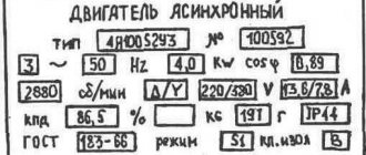
Let us depict the characteristics of the already considered transistor KT603A (Fig. 1.60).
Now the Earley effect manifests itself in the fact that as the voltage uke increases, the characteristics shift to the right. The differential resistance is now determined by the expression rdif= (dube/dib) |ib– given, uke= const
Output characteristics for a common emitter circuit
Let us depict these characteristics for the KT603A transistor (Fig. 1.61).
Let us turn to the previously obtained expression ik=αst·ie+iko In accordance with Kirchhoff's first law ie=ic+ib and taking into account the previous expression we obtain ikαst· (ic+ib) +icо from where ik=αst/ (1 -αst) ·ib + 1 / (1 -αst) iko
Let us introduce the notation: βst ≡ αst / (1- αst )
The coefficient αst is called the static transfer coefficient of the base current. Its value is usually tens - hundreds (this is a dimensionless coefficient).
It is easy to see that 1 / (1 -αst) = βst + 1 Let us introduce the designation i′ko ≡ (βst + 1) ·iko As a result, we obtain iк= βst ·ib+i′ko This expression, to a first approximation, describes the output characteristics in the active region work without taking into account the slope of the characteristics.
To take into account the slope, the expression is written in the form ik= βst ·ib+i′ko +ukb· ( 1 /r′к), where r′к =duke/dik|uke – given, ib=const
To a first approximation, r′k = ( 1 / 1 + βst) · rk (resistance rk is defined above). The so-called differential base current transfer coefficient β is often used.
To increase the collector current ∆iк and base current ∆ib, we can write:
∆iк ≈ β ∆ iб
By definition β=diк/diб|iк – given, uke=const
For the KT603A transistor at t = 25°C β = 10...80.
The value of β depends on the operating mode of the transistor. Let us present a typical graph of the dependence of β on the emitter current (it is almost equal to the collector current) for ukb = 2 V (Fig. 1.62).
For normal operation of the transistor at direct current, in addition to the condition Pk < Pk max discussed above, the conditions ik must be met
For the KT603A transistor discussed above, ik max = 300 mA, uke max = 30 V (at t < 70 ° C).
Let us schematically depict on the output characteristics for a circuit with a common emitter the so-called safe operation area in which the specified conditions are met (Fig. 1.63).
It is usually acceptable to assume (with some error) that the output characteristics for a circuit with a common emitter are located on straight segments fan-shaped from one point on the voltage axis (Fig. 1.64).
The voltage Ue (this is a positive value) is called the Early voltage. For transistor KT603A Ue ~ 40 V.