Before we start testing field-effect transistors, let’s consider what types of field-effect transistors there are.
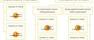
In Figure 1 you see the classification of field-effect transistors.
From this figure it can be seen that field-effect transistors are divided into transistors with a control pn junction and field-effect transistors with an insulated gate.
In foreign literature, a field-effect transistor with a control pn junction is designated as JFET
(junction gate field-effect transistor), and an insulated gate transistor is
a MOSFET
(Metall-Oxid-Semiconductor FET).
Today I will tell you how to test a field-effect transistor with a control pn junction
, and in the next issue of the magazine we will move on to testing the MOSFET transistor, so don’t forget to subscribe to the magazine. Subscription form after the article.
First, let's briefly look at the structure of the transistor and the principle of its operation.
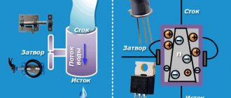
Field effect transistors are available in n-channel and p-channel types. In view of the fact that n-channel field-effect transistors have become widespread, using their example we will consider the operating principle of field-effect transistors with a control pn junction.
So, the transistor consists of an n-semiconductor with highly doped n-regions embedded in it with a high concentration of charge carriers - electrons. The semiconductor itself is located on a p-type substrate, which is connected to another p-type region. Together these areas are called the gate
(gate). Thus, each highly doped n-region creates its own pn junction with the p-substrate.
That part of the n-semiconductor that is located between the p-regions (gates) is called a channel (in particular, an n-type channel).
If a voltage source is connected to the highly doped n-regions, an electric field will be created in the channel; under the influence of this field, electrons from the n-region to which the “minus” of the source is connected will move to the n-region to which the “plus” of the voltage source is connected. Thus, an electric current will flow through the channel. The magnitude of this current will directly depend on the electrical conductivity of the channel, which in turn depends on the cross-sectional area of the channel. It is not difficult to guess that the cross-sectional area of the channel depends on the width of the pn junctions.
The region from which charge carriers move, and in the case of the n-channel these are electrons, is called the source
(source), and towards which they are moving -
drain
(drain).
If a negative voltage is applied to the gate relative to the source, then the pn junction formed between the gate and source will be biased in the opposite direction, while the width of the blocking layer will increase, thereby narrowing the size of the channel and reducing electrical conductivity.
Thus, by varying the voltage between gate and source, we can control the current through the FET channel.
That’s all about the design of a field-effect transistor; I won’t go into details further, since this will be enough to understand how to test a field-effect transistor with a control pn junction.
Based on the above, you can create an equivalent circuit of a field-effect transistor with a control pn junction, as we did when checking a bipolar transistor.
When drawing up a diagram, we will be guided by the following principles:
1. The transistor has two pn junctions, the first between the gate and the source, the second between the gate and the drain.
2. The channel between the source and drain, in the absence of a negative blocking voltage at the gate, is not closed and is electrically conductive, that is, it has a certain resistance value.
3. Now we will denote pn junctions by diodes, and the electrical conductivity of the channel by a resistor.
We make an equivalent circuit of a field-effect transistor with a control pn junction.
Now, knowing the equivalent circuit of a field-effect transistor with a control pn junction, you can build an algorithm or circuit for testing a field-effect transistor.
Checking a field-effect transistor with a control pn junction and an n-type channel.
1. Checking the channel resistance (in Fig. R)
To check the channel resistance using a multimeter, you must set the device to resistance measurement mode, the measurement limit is 2000 Ohms.
Measure the resistance between the source and drain of the transistor with different polarities of connecting the multimeter probes.
The channel resistance values with different polarities of connecting the probes should be approximately the same.
2. Checking the pn junction of the source-gate (in Fig. VD1).
Turn on the multimeter in diode testing mode. We connect the red (positive) probe of the multimeter to the gate (it has p-conductivity), and the black probe to the source. The multimeter should show the voltage drop across the open pn junction, which should be in the range of 600-700 mV.
We change the polarity of connecting the probes (red to source, black to gate), the multimeter, if the transistor is working properly, shows infinity (on the display “1”), that is, the transition is turned on in the opposite direction and is closed.
3. Checking the drain-gate pn junction (in Fig. VD2).
We also check the serviceability of the drain-gate pn junction. That is, we turn on the multimeter in diode testing mode. We connect the red (positive) probe of the multimeter to the gate (it has p-conductivity), and the black probe to the drain. The multimeter should show the voltage drop across the open gate-drain pn junction, which should be in the range of 600-700 mV.
We change the polarity of connecting the probes (red to drain, black to gate), the multimeter, if the transistor is working properly, shows infinity (on the display “1”), that is, the transition is turned on in the opposite direction and is closed.
If all three conditions are met, then the field-effect transistor is considered to be working.
Choosing circuit component ratings
To select the required component ratings, you need to know another important transistor parameter - the gain.
When current flows from the base to the emitter, the transistor turns on so that more current can flow from the collector to the emitter.
There is a relationship between the magnitudes of these two currents. This is called transistor gain. For a general purpose transistor such as the BC547 or 2N3904, the gain averages around 100. This means that if you apply 0.1 mA current to the base-emitter junction, then in the collector-emitter direction you will receive a current of 10 mA (at 100 times more).
What should be the resistance of resistor R1 to obtain a current of 0.1 mA?
If we have a 9V battery as a power source and we know that the voltage drop across the base-emitter junction is 0.7V, then there will be 8.3V left across the resistor. To find the resistance of the resistor you can use Ohm's law:
That is, you need to use a resistor with a resistance of 83 kOhm. This is not a standard value, so from the standard nominal series we will take the closest value equal to 82 kOhm.
Resistor R2 is designed to limit the current passing through the LED. A resistance of 1 kOhm will be sufficient.
Checking a field-effect transistor with a control pn junction and a p-type channel.
Testing a field-effect transistor with a control pn junction and a p-type channel is carried out according to the above algorithm, except that when checking pn junctions, the polarity of connecting the multimeter probes is reversed.
For clarity and ease of understanding of the process, I recorded a video for you on how to check a field-effect transistor with a control pn junction, where I check a transistor with a p-type channel.
In technology and amateur radio practice, field-effect transistors are often used. Such devices differ from conventional bipolar transistors in that in them the output signal is controlled by a control electric field. Insulated gate field effect transistors are especially often used.
The English designation for such transistors is MOSFET, which means “field-controlled metal-oxide semiconductor transistor.” In the domestic literature, these devices are often called MOS or MOS transistors. Depending on the manufacturing technology, such transistors can be n- or p-channel.
An n-channel type transistor consists of a silicon substrate with p-conductivity, n-regions obtained by adding impurities to the substrate, and a dielectric that insulates the gate from the channel located between the n-regions. The pins (source and drain) are connected to the n-regions. Under the influence of a power source, current can flow from source to drain through the transistor. The magnitude of this current is controlled by the insulated gate of the device.
When working with field-effect transistors, it is necessary to take into account their sensitivity to the effects of an electric field. Therefore, they must be stored with the terminals short-circuited with foil, and before soldering, the terminals must be short-circuited with a wire. Field-effect transistors must be soldered using a soldering station, which provides protection against static electricity.
Before you start checking the serviceability of the field-effect transistor, you need to determine its pinout. Often, on an imported device, marks are applied that identify the corresponding terminals of the transistor.
The letter G denotes the gate of the device, the letter S the source, and the letter D the drain.
If there is no pinout on the device, you must look it up in the documentation for this device.
Electronics for everyone
Except transistors
Darlington
assemblies, there is another good way to drive a powerful constant load -
MOSFETs . A field-effect transistor operates like a conventional transistor - a weak signal at the gate controls a powerful flow through the channel. But, unlike bipolar transistors, here the control is not by current, but by voltage .
MOS (in bourgeois MOSFET ) stands for Metal-Oxide-Semiconductor; from this abbreviation the structure of this transistor becomes clear.
If on the fingers, then it has a semiconductor channel that serves as one plate of the capacitor and the second plate is a metal electrode located through a thin layer of silicon oxide, which is a dielectric. When voltage is applied to the gate, this capacitor is charged, and the electric field of the gate pulls charges to the channel, as a result of which mobile charges appear in the channel that can form an electric current and the drain-source resistance drops sharply. The higher the voltage, the more charges and lower the resistance, as a result, the resistance can drop to tiny values - hundredths of an ohm, and if you raise the voltage further, a breakdown of the oxide layer and the Khan transistor will occur. The advantage of such a transistor, compared to a bipolar one, is obvious - voltage must be applied to the gate, but since there is a dielectric, the current will be zero, which means the required power to control this transistor will be negligible; in fact, it consumes only at the moment of switching, when charging is in progress and capacitor discharge.
The disadvantage arises from its capacitive property - the presence of capacitance on the gate requires a large charging current when opening. In theory, equal to infinity on infinitely small periods of time. And if the current is limited by a resistor, then the capacitor will charge slowly - there is no escape from the time constant of the RC circuit.
MOS transistors come in P and N channel. They have the same principle, the only difference is the polarity of the current carriers in the channel. Accordingly, in different directions of the control voltage and inclusion in the circuit. Very often transistors are made in the form of complementary pairs. That is, there are two models with exactly the same characteristics, but one of them is N channel, and the other is P channel. Their markings, as a rule, differ by one digit.
The load is connected to the drain circuit. In general, in theory, it makes no difference to a field-effect transistor what is considered a source and what is a drain - there is no difference between them. But in practice there is, the fact is that to improve the characteristics, the source and drain are made of different sizes and designs, plus, in powerful field devices there is often a reverse diode (it is also called parasitic, because it is formed by itself due to the peculiarities of the technical process production).
My most popular MOS transistors are IRF630 (n channel) and IRF9630 (p channel). At one time I installed about a dozen of each type. Possessing a not very large TO-92 , this transistor can easily pull through itself up to 9A. Its open resistance is only 0.35 Ohm. However, this is a rather old transistor; now there are better things, for example IRF7314 , capable of carrying the same 9A, but at the same time it fits into an SO8 case - the size of a notebook square.
One of the problems of joining MOSFET transistor and a microcontroller (or digital circuit) is that in order to fully open until completely saturated, this transistor needs to drive quite a higher voltage to the gate. Usually this is about 10 volts, and the MK can output a maximum of 5. There are three options:
- Using smaller transistors, build a chain that supplies power from the high-voltage circuit to the gate in order to pump it with high voltage
- use a special driver chip, which itself will generate the required control signal and equalize the levels between the controller and the transistor. Typical examples of drivers are, for example, IR2117.
You just need to remember that there are upper and lower shoulder drivers (or combined, half-bridge). The choice of driver depends on the load connection circuit and the switching transistor. If you pay attention, you will see that N channel transistors are used with the driver in both the upper and lower arms. They just have better characteristics than P channel ones. But here another problem arises. In order to open the N channel transistor in the upper side, it needs to apply a voltage higher than the drain voltage to its gate, and this, in fact, is higher than the supply voltage. To achieve this, a voltage pump is used in the high-side driver. What exactly is the difference between a lower shoulder driver and an upper shoulder driver?
- Use a transistor with a low turn-on voltage. For example, from the IRL630A series or the like. Their opening voltages are tied to logical levels. They do have one drawback - they are sometimes difficult to get. If ordinary powerful field workers are no longer a problem, then those controlled by the logical level are not always the case.
But in general, it is more correct to install a driver, because in addition to the main functions of generating control signals, it also provides current protection, protection against breakdown, overvoltage, as an additional bauble, optimizes the opening speed to the maximum, in general, it does not consume its current in vain.
Choosing a transistor is also not very difficult, especially if you don’t bother with limiting modes. First of all, you should be concerned about the value of the drain current - I Drain or ID; you select a transistor based on the maximum current for your load, preferably with a margin of 10 percent. The next important parameter for you is VGS - Source-Gate saturation voltage or, more simply put, control voltage. Sometimes it is written, but more often you have to look at the charts. You are looking for a graph of the output characteristics Dependence of ID on VDS at different values of VGS . And you figure out what kind of regime you will have.
For example, you need to power the engine at 12 volts, with a current of 8A. You screwed up the driver and only have a 5 volt control signal. The first thing that came to mind after this article was IRF630. The current is suitable with a margin of 9A versus the required 8. But let’s look at the output characteristic:
You see, at 5 volts on the gate and a current of 8A, the voltage drop across the transistor will be about 4.5V. According to Ohm's law, then it turns out that the resistance of this transistor at the moment is 4.5/8 = 0.56 Ohm . Now let’s calculate the power losses - your engine consumes 5A. P=I*U or, if we apply the same Ohm's law, P=I2R . At 8 amperes and 0.56 Ohm the loss will be 35 W. It hurts a lot, don't you think? I also think it’s too much. the IRL630 then .
At 8 amps and 5 volts on the Gate, the voltage across the transistor will be about 3 volts. Which will give us 0.37 Ohm and 23 W losses, which is noticeably less.
If you are going to use PWM on this switch, then you need to inquire about the opening and closing times of the transistor, choose the largest one and, relative to the time, calculate the maximum frequency of which it is capable. This value is called Switch Delay or ton , toff , in general, something like that. Well, the frequency is 1/t. It would also be a good idea to look at the gate capacitance Ciss , based on it, as well as the limiting resistor in the gate circuit, you can calculate the charging time constant of the RC gate circuit and estimate the performance. If the time constant is greater than the PWM period, then the transistor will not open/close, but will hang in some intermediate state, since the voltage at its gate will be integrated by this RC circuit into a constant voltage.
When handling these transistors, take into account the fact that they are not just very afraid of static electricity, but VERY STRONG . It is more than possible to penetrate the shutter with a static charge. So when you buy it, immediately wrap it in foil and don’t take it out until you seal it. First ground yourself to the battery and put on a foil hat :).
And in the process of designing a circuit, remember one more simple rule - under no circumstances should you leave the field gate shutter hanging just like that - otherwise it will eat noise from the air and open on its own. Therefore, it is necessary to install a 10 kilo-ohm resistor from Gate to GND for N channel or +V for P channel, so that the parasitic charge flows off. That seems to be all, next time I’ll write about bridge circuits for controlling engines.
Circuit for checking an n-channel field-effect transistor with a multimeter
Before checking the serviceability of the field-effect transistor, it is necessary to take into account that in modern MOSFET-type radio components there is an additional diode between the drain and the source. This element is usually present on the device diagram. Its polarity depends on the type of transistor.
The general rules are to begin the procedure by determining the performance of the measuring device itself. Having made sure that it works flawlessly, they move on to further measurements.
Conclusions:
- MOSFET field-effect transistors are widely used in technology and amateur radio practice.
- The performance of such transistors can be checked using a multimeter, following a certain method.
- Testing a p-channel field-effect transistor with a multimeter is carried out in the same way as an n-channel transistor, except that the polarity of the multimeter leads should be reversed.
Why do you need a transistor?
I often have a question: why do we need a transistor? Why not connect the LED and resistor directly to the battery?
The advantage of a transistor is that you can use a small current or voltage to control a much larger current and voltage.
This is very useful if you want to control things like motors, high power LEDs, speakers, relays and more using a microcontroller/Raspberry Pi/Arduino. The output of the microcontroller can only provide a few milliamps at 5V. So if you want to control, for example, a 230V street light, you cannot do it directly with the microcontroller
You can use a relay instead. But even a relay usually requires more current than the microcontroller output can provide. Therefore you will need a transistor to drive the relay:
Video on how to test a field-effect transistor
Semiconductor elements are used in almost all electronic circuits. Those who call them the most important and most common radio components are absolutely right. But any components do not last forever; overvoltage and current, temperature violations and other factors can damage them. We will tell you (without overloading with theory) how to check the performance of various types of transistors (npn, pnp, polar and composite) using a tester or multimeter.
Before checking any element with a multimeter for serviceability, be it a transistor, thyristor, capacitor or resistor, it is necessary to determine its type and characteristics. This can be done by marking. Once you know it, it won’t be difficult to find a technical description (datasheet) on thematic sites. With its help, we will find out the type, pinout, main characteristics and other useful information, including replacement analogues.
For example, the scanning on the TV stopped working. Suspicion is raised by the line transistor marked D2499 (by the way, a fairly common case). Having found a specification on the Internet (a fragment of it is shown in Figure 2), we receive all the information necessary for testing.
Figure 2. Specification fragment for 2SD2499
There is a high probability that the datasheet found will be in English, no problem, the technical text is easy to understand even without knowledge of the language.
Having determined the type and pinout, we solder the part and begin testing. Below are the instructions with which we will test the most common semiconductor elements.
Driver chip selection criteria
Let's look at an example of choosing a driver for the CoolSiC IMW120R045M1 transistor manufactured by Infineon. Table 2 shows the information from the transistor specification necessary to select a driver.
Table 2. Fragment of the specification of the transistor IMW120R045M1
| Limit values | |||
| Parameter | Symbol | Magnitude | |
| Drain-source voltage, V | VDSS | 1200 | |
| The drain current for Rth(jc,max) is limited to Tvjmax, VGS = 15 V, A | TC = 25°C | ID | 52 |
| TC = 100°C | 36 | ||
| Gate-Source Voltage | VGSS | -10/+20* | |
| * – A bipolar gate driver can be used. | |||
The choice of positive and negative gate voltages affects the life of the device. To ensure the required service life, the recommendations described in AN 2018-19 should be taken into account.
To select a negative gate voltage, we will use the graph (Figure 13) from AN 2018-19 for a positive gate voltage VCC2 = 15 V, although the IMW120R045M1 transistor can operate at a voltage VCC2 = 18 V.
Rice. 13. Selection of negative gate voltage according to AN 2018-19
The normalized switching frequency depends on the service life of the device and is calculated using formula 8:
$$Nf_{SW}=\frac{Af_{SW}\times T_{S}\times OT}{10},\qquad{\mathrm{(}}{8}{\mathrm{)}}$$
Where:
- NfSW – normalized switching frequency, kHz;
- AfSW – actual switching frequency, kHz;
- Ts – device service life, years
- OT – percentage of working time of the total, %
Thus, the greater the negative voltage, the shorter the normalized frequency and, accordingly, the service life of the device.
According to Figure 13, for a normalized frequency of 100 kHz, a negative voltage VEE2 = -2.8 V is obtained. However, lower voltages can be used. The minimum voltage VEE2 must be such that the RDS(on) resistance increases by no more than 15% at rated current and Tj = 125°C. In this example, to provide some safety margin, we will take VEE2 = -2 V.
External resistor RG,ext is calculated based on formula 9:
$$R_{G,ext}=\frac{V_{Drive}\times (t_{r}+t_{d(on)})}{Q_{Gate}},\qquad{\mathrm{(}}{ 9}{\mathrm{)}}$$
Where:
QGate is defined according to Figure 4;
- tr = 24‧10-9 s and td(on) = 9‧10-9 s (values are taken from the specification for the IMW120R045M1 transistor;
- VDrive = VCC2 – VEE2 = 17 V;
- QGate, according to Figure 4, is taken to be approximately 60‧10-9 C.
Thus we get RG,ext = 9.35 Ohm ≈ 10 Ohm.
Let's calculate the maximum gate current using formula 10 with RG,int = 4 Ohm, RG,ext = 10 Ohm, RDS(on) = 0 Ohm:
$$R_{G\_Total}=R_{DS(on)}+R_{G,ext}+R_{G,int};\\V_{Drive}=VCC2-VEE2;\:I_{Gmax}=\ frac{V_{Drive}}{R_{G\_Total}}\qquad{\mathrm{(}}{10}{\mathrm{)}}$$
Since the calculation is carried out for the first time and the value of RDS(on) is unknown, it is equal to zero.
We get IGmax ≈ 1.21 A.
Let's calculate the maximum power dissipation in the driver control circuit using formula 11:
$$P_{vtot}=Q_{G}\times dV_{Drive}\times f_{SW},\qquad{\mathrm{(}}{11}{\mathrm{)}}$$
Pvtot = 0.102 W.
It is important to fulfill the following conditions:
Pvtot ≤ PDOUT,
where PDOUT is the maximum output power of the driver according to the specification.
Based on the calculations, we select the appropriate driver produced by Infineon from Table 3.
Table 3. Recommended list of drivers for SiC MOSFETs
| Name, body | Typical peak control current, A | VCC2-VEE2, V | Typical propagation delay, ns | Active suppression of the Miller effect | Short circuit protection |
| 1EDI20I12MF | 3,5 | 20 | ≤300 | + | – |
| DSO-8 150mil | |||||
| 1EDC20H12AH | 3,5 | 40 | ≤125 | – | – |
| DSO-8 300mil | |||||
| 1EDC60H12AH | 9,4 | 40 | ≤125 | – | – |
| DSO-8 300mil | |||||
| 1EDC20I12MH | 3,5 | 20 | ≤300 | + | – |
| DSO-8 300mil | |||||
| 1ED020I12-F2 | 2 | 28 | ≤170 | + | + |
| DSO-16 300mil | |||||
| 2ED020I12-F2 | 2 | 28 | ≤170 | + | + |
| DSO-36 |
The most suitable driver for the example discussed in this section is the 1ED020I12-F2 chip.
Checking a bipolar transistor with a multimeter
This is the most common component, for example the KT315, KT361 series, etc.
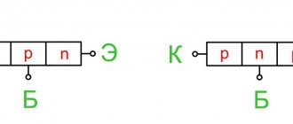
There will be no problems with testing this type; it is enough to imagine the pn junction as a diode. Then the pnp and npn structures will look like two counter- or reverse-connected diodes with a midpoint (see Fig. 3).
Figure 3. “Diode analogues” of pnp and npn junctions
We connect the probes to the multimeter, the black one to “COM” (this will be a minus), and the red one to the “VΩmA” socket (plus). We turn on the testing device, switch it to the dialing or resistance measurement mode (it is enough to set the limit to 2 kOhm), and begin testing. Let's start with pnp conductivity:
- We attach the black probe to terminal “B”, and the red one (from the “VΩmA” socket) to leg “E”. We look at the multimeter readings; it should display the value of the junction resistance. The normal range is 0.6 kOhm to 1.3 kOhm.
- In the same way we take measurements between terminals “B” and “K”. The readings should be in the same range.
If during the first and/or second measurement the multimeter displays minimum resistance, then there is a breakdown in the transition(s) and the part requires replacement.
- We reverse the polarity (red and black probe) and repeat the measurements. If the electronic component is working properly, the resistance will be displayed, tending to the minimum value. If the reading is “1” (the measured value exceeds the capabilities of the device), an internal break in the circuit can be stated, therefore, the radio element will need to be replaced.
Testing a reverse conduction device follows the same principle, with a slight modification:
- We connect the red probe to leg “B” and check the resistance with the black probe (touching terminals “K” and “E” in turn), it should be minimal.
- We change the polarity and repeat the measurements, the multimeter will show a resistance in the range of 0.6-1.3 kOhm.
Deviations from these values indicate a component failure.
Checking the functionality of the field-effect transistor
This type of semiconductor elements is also called mosfet and mosfet components. Figure 4 shows the graphic designation of n- and p-channel field switches in circuit diagrams.
Figure 4. Field-effect transistors (N- and P-channel)
To test these devices, we connect the probes to the multimeter in the same way as when testing bipolar semiconductors, and set the test type to “continuity”. Next, we proceed according to the following algorithm (for an n-channel element):
- We touch the black wire to the “c” pin, and the red wire to the “i” pin. The resistance on the built-in diode will be displayed, remember the reading.
- Now you need to “open” the transition (this will only be possible partially), for this we connect the probe with the red wire to terminal “z”.
- We repeat the measurement carried out in step 1, the reading will change downwards, which indicates a partial “opening” of the field worker.
- Now you need to “close” the component, for this purpose we connect the negative probe (black wire) to the “z” leg.
- We repeat steps 1, the original value will be displayed, therefore, “closing” has occurred, which indicates the serviceability of the component.
To test p-channel elements, the sequence of actions remains the same, with the exception of the polarity of the probes, it must be reversed.
Note that insulated gate bipolar elements (IGBT) are tested in the same way as described above. Figure 5 shows the SC12850 component in this class.
Fig 5. IGBT transistor SC12850
For testing, it is necessary to perform the same steps as for a field-effect semiconductor element, taking into account that the drain and source of the latter will correspond to the collector and emitter.
In some cases, the potential on the multimeter probes may not be enough (for example, to “open” a powerful power transistor); in such a situation, additional power will be needed (12 volts will be enough). It must be connected through a resistance of 1500-2000 Ohms.
What types of transistors are there?
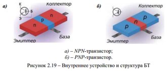
We will not take you on a long excursion into how it all began, that vacuum tubes were the grandfathers and grandmothers of modern transistors. Let's not talk about electronic emission. That the process in these same lamps is similar to transistors. We will not describe the differences between them. We'll get straight to the main point. Hoping that everything we missed, although it will remain a dark spot, will not become a burdensome circumstance preventing us from understanding how the transistor actually works. So, transistors are bipolar and field-effect. The essence of the work of both is the same, except that their crystals, or rather how different types of crystals are fused, are different.
In bipolar transistors, this is a kind of hamburger, if you want pie: pnp or npn. That is, crystals with different conductivities are soldered in series with each other. In this way they form a kind of “sandwich”.
Field-effect transistors also have an n crystal and a p crystal, but they are not soldered in series, but in parallel. In this case, the current does not pass through different types of conductivity of the crystals, but always follows one type. And in this case, the conductive crystal is locked using the electric field of the control gate. Hence the name field.
There are also low-frequency, mid-frequency and high-frequency transistors. They can also work with different currents, but these are all nuances...
Checking a Composite Transistor
Such a semiconductor element is also called a “Darlington transistor”; in fact, it is two elements assembled in one package. For example, Figure 6 shows a fragment of the specification for KT827A, which displays the equivalent circuit of its device.
Figure 6. Equivalent circuit of the KT827A transistor
It will not be possible to check such an element with a multimeter; you will need to make a simple probe, its diagram is shown in Figure 7.
Rice. 7. Circuit for testing a composite transistor
Designation:
- T is the element being tested, in our case KT827A.
- L – light bulb.
- R is a resistor, its value is calculated using the formula h21E*U/I, that is, we multiply the input voltage by the minimum gain value (for KT827A - 750), divide the resulting result by the load current. Let's say we use a light bulb from the side lights of a car with a power of 5 W, the load current will be 0.42 A (5/12). Therefore, we will need a 21 kOhm resistor (750 * 12 / 0.42).
Testing is carried out as follows:
- We connect the plus from the source to the base, as a result the light bulb should light up.
- We apply minus - the light goes out.
This result indicates the functionality of the radio component; other results will require replacement.
Types of transistors
Each branch differs by 0.
Image of field triode wiring diagrams Almost every circuit is capable of operating at very low input voltages. MOSFET connection circuit The traditional, classic connection circuit of a “mosfet” operating in the open-close switch mode is shown in Fig. 3.
Tests have shown that the transistor switch works perfectly, supplying voltage to the load. Transistors are voltage controlled and do not consume control current in static conditions.
If a voltage is applied to such a transistor, plus to the drain and minus to the source, a large current will flow through it, it will be limited only by the channel resistance, external resistances and internal resistance of the power source. This means that you need to avoid this by introducing a stage with a high input impedance. Among them are: bipolar transistors with embedded resistors and their circuitry; combinations of two triodes of the same or different structures in one package; lambda diodes - a combination of two field-effect triodes forming a section with negative resistance; designs in which a field-effect triode with an insulated gate drives a bipolar triode are used to control electric motors. To prevent the alternating voltage component from being released across the resistor Ri, it is shunted with a capacitor Ci.
The common source cascade gives a very large current and power amplification. The potential difference reaches a value from 0.3 to 0.6 V. Only the arrows on the conventional image of field-effect transistors have the direction exactly opposite to their bipolar counterparts.
This means that you need to avoid this by introducing a stage with a high input impedance. Stability under temperature changes. At a certain voltage Uс, the channel narrows, at which the boundaries of both pn junctions narrow and the channel resistance becomes high. This is possible due to the fact that injection of minority charge carriers is not used.
Principle of operation of a triode When the base is de-energized, the transistor very quickly returns to its original state and the collector junction closes. Therefore, the use of this approach in practice is strongly limited in amplification technology.
An oscillation amplifier is also connected here. The gate function is performed by a metal lead, which is separated from the crystal by a layer of dielectric and, thus, is not in electrical contact with it. Reverse polarity protection based on field-effect transistor