How to test a transistor without desoldering it from the circuit
Desoldering a certain element from a circuit involves some difficulties - it is difficult to determine from its appearance which one needs to be desoldered.
Many professionals suggest using a probe to test the transistor directly in the socket. This device is a blocking generator, in which the role of the active element is played by the part itself that requires testing.
The system of operation of the probe with a complex circuit is based on the inclusion of 2 indicators that indicate whether the circuit is broken or not. Options for their manufacture are widely presented on the Internet.
The sequence of actions when checking transistors with one of these devices is as follows:
- First, a working transistor is tested, with the help of which it is checked whether there is current generation or not. If there is generation, then we continue testing. In the absence of generation, the winding terminals are swapped.
- Next, lamp L1 is checked for open circuit probes. The light should be on. If this does not happen, the terminals of any of the transformer windings are swapped.
- After these procedures, the device begins directly checking the transistor, which is supposedly out of order. Probes are connected to its terminals.
- The switch is set to the PNP or NPN position and the power is turned on.
The glow of lamp L1 indicates the suitability of the circuit element being tested. If lamp L2 starts to light, then there is some problem (most likely the junction between the collector and the emitter is broken);
There are also probes with very simple circuits that do not require any adjustment before starting work. They are characterized by a very small current that passes through the element to be tested. At the same time, the danger of its failure is practically zero.
This category includes devices consisting of a battery and a light bulb (or LED).
To check, you need to perform the following operations sequentially:
- Connect one of the probes to the most likely output of the base.
- Using the second probe, we touch each of the remaining two terminals in turn. If there is no contact in one of the connections, then an error occurred with the selection of the base. You need to start over with a different order.
- Next, it is advised to perform the same operations with another probe (change positive to negative) on the selected base.
- Alternately connecting the base with probes of different polarities to the collector and emitter should fix the contact in one case, but not in the other. It is believed that such a transistor is working.
How to check the field effect transistor KP303? (The electret microphone does not work
Maybe there is such a way? Otherwise, I can’t get the MKE-30 electret microphone to work. I can’t, that’s all. I tried everything. I have 5 of these KP303. but in these tests I may have killed them.
After all, they must be grounded when soldering, all four legs must be short-circuited. remove static tension from yourself. So I don’t know if they are alive. To press the microphone. He hesitated. It hasn't started for ages.
The element itself died. They have a limited lifespan. Although the electret should “live” for 30 years.
The drop itself?! And I thought that there were only two membranes, precisely located and distanced from each other. This is it. not a mechanism. to break.
But the head (capsule) is really old. And the size is much larger than the current ones that are sold. I assumed that this one had a better size and frequency.
And at the same time, I’ll ask. These transistors are not found in our radio components. They do not sell domestic parts. But not about that
I also wanted to buy the most economical blue LEDs. And there is only one type. It costs 8 rubles. The type of LED on the receipt is listed as GNL 5013BW (although the saleswoman dictated it to me as L 5013BC)
Is it economical? I need a circuit powered by the crown.
This is for purely capacitor ones. And for electret ones. //cxem.net/sprav/sprav96.php
PS. The smaller the distance between the membrane and the electrode, the smaller the diameter of the capsule. Technologically difficult task. For our drunks.
“Electret microphones operate on the same principle as condenser microphones, but the constant voltage in them is provided by the electret charge, which is applied in a thin layer to the membrane and retains this charge for a long time (over 30 years).”
Really. there is something temporary in them. Only about 30 years is a Jewish exaggeration. Ehh. it means it won't work. Are such heads produced now? With a fresh charge of electret? What would be bigger in diameter?
For music. Voice and sound recordings. I want frequencies, lenses.
For studio recordings, these expectations are naturally unreasonable. But. I want to listen. experiment.
And the power supply for such microphones is 48 volts. (and there is no battery compartment)
So. It seems to me that you should not ignore the quality of the capsule.
Although I. Interesting opinions on this. Maybe these capsules are potentially good. We just need to create conditions for the manifestation of this potential.
Expert opinion
Viktor Pavlovich Strebizh, lighting and electrical expert
Any questions ask me, I will help!
If you are lucky enough to become the owner of a rare MIS device without a structural diode, then, accordingly, the structural diode check described below does not make sense. If there is something you don’t understand, write to me!
Checking a Composite Transistor
Such a semiconductor element is also called a “Darlington transistor”; in fact, it is two elements assembled in one package. For example, Figure 6 shows a fragment of the specification for KT827A, which displays the equivalent circuit of its device.
Figure 6. Equivalent circuit of the KT827A transistor
It will not be possible to check such an element with a multimeter; you will need to make a simple probe, its diagram is shown in Figure 7.
Rice. 7. Circuit for testing a composite transistor
Designation:
- T is the element being tested, in our case KT827A.
- L – light bulb.
- R is a resistor, its value is calculated using the formula h21E*U/I, that is, we multiply the input voltage by the minimum gain value (for KT827A - 750), divide the resulting result by the load current. Let's say we use a light bulb from the side lights of a car with a power of 5 W, the load current will be 0.42 A (5/12). Therefore, we will need a 21 kOhm resistor (750 * 12 / 0.42).
Testing is carried out as follows:
- We connect the plus from the source to the base, as a result the light bulb should light up.
- We apply minus - the light goes out.
This result indicates the functionality of the radio component; other results will require replacement.
Checking thyristors on the multimeter connector for transistors
Many people are interested in whether it is possible to test a thyristor with a multimeter using the standard socket for testing transistors on the front panel, designated pnp/npn. The answer is yes. You just need to apply the correct voltage. The gain shown on the display will most likely be incorrect. Therefore, avoid being guided by numbers. Let's see how it's done. If the thyristor opens with a positive potential, it must be connected to pin B (base) of the npn half-socket. The anode is plugged into pin C (collector), the cathode is plugged into pin E (emitter). It is unlikely that it will be possible to test a powerful thyristor with a multimeter; for microelectronics, the technique will work.
Field device test
The procedure for such elements is similar to bipolar ones. However, there are some peculiarities here:
- If the positive probe is applied to the multimeter, and the negative one to the source, then the capacitance is charged and the junction opens.
- Before checking the drain-source channel, short circuit all terminals to discharge the capacitance. The resistances are increased again and you can test them again with a multimeter.
- Internal diodes are often installed. During the procedure, the properties of the semiconductor device are revealed.
- For the reason stated above, you need to make sure that the diode is present so that the measurement takes place without errors.
- After the first process, the probes are swapped. The display will show one, indicating infinite resistance. Otherwise, the transistor is faulty.
Due to these points, it is possible to carry out a high-quality check of field devices without involving desoldering. If you have a composite device, then the test is similar to the procedure for bipolar devices.
Basic ways to check a transistor
The transistor is a very important element in most radio circuits. Those who decide to engage in radio modeling must first of all know how to test them and what devices to use.
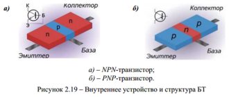
A bipolar transistor has 2 PN junctions. The outputs from it are called emitter, collector and base. The emitter and collector are elements located at the edges, and the base is located between them, in the middle. If we consider the classical scheme of current movement, then it first enters the emitter and then accumulates in the collector. The base is necessary in order to regulate the current in the collector.
Signs of trouble
Now we know how to determine a working transistor, but how to check a transistor with a multimeter and find out that it is not working? Here, too, everything is quite easy and simple. The first malfunction of the element is expressed in the absence of a voltage drop or in an infinitely large resistance of the direct and reverse pn junction.
That is, when dialing, the device shows “1”. This means that the measured transition is open and the element is not working. Another malfunction of the element is expressed in the presence of a large voltage drop on the semiconductor (the device usually beeps), or near zero resistance values of the forward and reverse pn junctions. In this case, the internal structure of the element is broken (short-circuited), and it is not working.
Determining the pinout of a transistor
Now let's learn how to determine where the base, emitter and collector are located on a transistor. First of all, they begin to look for the base of the element. To do this, turn on the multimeter in dialing mode.
We attach the positive probe to the left leg, and with the negative probe we sequentially measure on the middle and right leg. The multimeter showed us “1” between the left and middle legs, and between the left and right legs the readings were 555 mV.
So far, these measurements do not allow us to draw any conclusions. Let's move forward. We fix the positive probe on the middle leg, and sequentially measure with the minus probe on the left and right legs. The toaster showed a value of "1" between the left and middle legs, and 551 mV between the middle and right legs.
Testing the diode with a multimeter.
These measurements also do not make it possible to draw a conclusion and determine the base. Let's move on. We fix the plus probe on the right leg, and with the minus probe we fix the middle and left leg in turn, while taking measurements. During the measurement, we see that the voltage drop between the right and middle legs is equal to one, and between the right and left legs is also equal to one (infinity). Thus, we have found the base of the transistor, and it is located on the right leg.
Now we just have to determine which leg is the collector and which leg is the emitter. To do this, the device should be switched to measuring resistance of 200 kOhm. We measure on the middle and left leg, for which we will fix the probe with a minus on the right leg (base), and we will fix the positive one in turn on the middle and left legs, while measuring the resistance.
Having received the measurements, we see that on the left leg R = 121.0 kOhm, and on the middle leg R = 116.4 kOhm. You should remember once and for all, if you subsequently check and find the emitter and collector, that the resistance of the collector junction is in all cases less than the resistance of the emitter.
Checking the varistor for serviceability with a multimeter and without a tester
Causes of malfunction
Varistors are installed in parallel with the protected circuit, and a fuse is placed in series with it. This is necessary so that when the varistor burns out, if the overvoltage pulse is too strong, the fuse will burn out, and not the tracks of the printed circuit board.
The only reason for the failure of a varistor is a sudden and strong voltage surge in the network. If the energy of this jump is greater than the varistor can dissipate, it will fail. The maximum energy dissipation depends on the dimensions of the component. They differ in diameter and thickness, that is, the larger they are, the more energy the varistor can dissipate.
Voltage surges can occur during accidents on power lines, during a thunderstorm, or when switching powerful devices, especially inductive loads.
Verification methods
Any repair of electronics and electrical equipment begins with an external inspection, and then proceeds to measurements. This approach allows you to localize most faults. To find a varistor on the board, look at the figure below - this is what varistors look like. Sometimes they can be confused with capacitors, but can be distinguished by their markings.
If the element is burnt out and the markings cannot be read, look at this information on the device diagram. On the board and in the diagram it can be designated by the letters RU. The conventional graphic symbol looks like this.
There are three ways to test a varistor quickly and easily:
- Visual inspection.
- Call. This can be done with a multimeter or any other device that has a continuity test function.
- Resistance measurement. This can be done with a high-range ohmmeter, multimeter or megger.
A varistor fails when a large or prolonged current passes through it. Then the energy is dissipated in the form of heat, and if its amount is greater than that determined by the design, the element burns out. The housing of these components is made of a hard dielectric material, such as ceramic or epoxy coating. Therefore, when it fails, the integrity of the outer coating is most often damaged.
You can visually check the varistor for functionality - there should be no cracks on it, as in the photo:
The next method is to check the varistor with a tester in continuity mode. This cannot be done in the circuit, because the dialing can work through parallel-connected elements. Therefore, you need to unsolder at least one of its legs from the board.
Important: you should not check the elements for serviceability without desoldering them from the board - this may give false readings from the measuring instruments. Since in the normal state (without voltage applied to the terminals) the resistance of the varistor is high, it should not ring through. The test is performed in both directions, that is, by swapping the multimeter probes twice
The test is performed in both directions, that is, by swapping the multimeter probes twice
Since in the normal state (without voltage applied to the terminals) the resistance of the varistor is high, it should not ring through. The test is performed in both directions, that is, by swapping the multimeter probes twice.
On most multimeters, the continuity mode is combined with the diode testing mode. It can be found by the diode icon on the mode selector scale. If there is a sound indication sign next to it, it probably also has a dial tone.
Another way to test a varistor for breakdown with a multimeter is to measure the resistance. You need to set the device to the maximum measurement limit, in most devices this is 2 MOhms (megaohms, designated as 2M or 2000K). The resistance must be equal to infinity. In practice, it can be lower, within 1-2 MOhm.
Interesting! The same can be done with a megaohmmeter, but not everyone has one. It is worth noting that the voltage at the megohmmeter terminals should not exceed the classification voltage of the component being tested.
This ends the available methods for checking a varistor. This time, the multimeter will help the radio amateur find the faulty element, as in a large number of other cases. Although in practice a multimeter is not always needed in this matter, because the matter rarely goes beyond a visual inspection. Replace the burnt element with a new one, designed for voltage and with a diameter no less than the burnt one, otherwise it will burn out even faster than the previous one.
How does it work
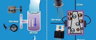
The field-effect transistor differs from other varieties in the features of its device. It can be one of two types:
- with control transition;
- with insulated shutter.
The first of them are n channel and p channel. The first of them are more common. They use the following operating principle. A semiconductor with n-conductivity is used as a basis.
The source and drain contacts are connected to it on opposite sides. In the middle part, on opposite sides, there are inclusions of a conductor with p-conductivity - they are a gate. The part of the semiconductor that is between them is a channel.
If a potential difference is applied to the source and drain of an n channel transistor, then current will flow. However, when a negative voltage is applied to the gate relative to the source, the channel width for electron movement will decrease. As a result, the current strength will become less.
Thus, by decreasing or increasing the width of the channel, it is possible to regulate the current strength between the source and drain or isolate them from each other. In p-channel transistors, the operating principle will be similar.
This type of FET is becoming less common, and is being replaced by those that use an insulated gate. They can be one of two types: npn or pnp. Their operating principle is similar. The first of them will be discussed here in more detail: npn.
In this case, a p-type semiconductor is used as the basis for the transistor. Two parallel strips of semiconductor with a different type of main charge carriers are built into it. An insulator is laid between them on the surface, and a layer of conductor is installed on top. This part is the gate, and the strips are the source and drain.
When a positive voltage is applied to the gate relative to the source, a positive charge is applied to the plate, creating an electric field. It attracts positive charges to the surface, creating a channel for current to flow between source and drain.
The higher the voltage applied to the gate, the higher the current flows between the source and drain. For all types of field-effect transistors, control occurs by applying voltage to the gate.
Types of electron and hole transitions.
What malfunctions occur
Field-effect transistors can be overloaded with current during testing and, as a result of overheating, become faulty.
Important! They are vulnerable to static voltage. During the work, you need to ensure that it does not fall on the part being tested.
When working as part of a circuit, a breakdown may occur, as a result of which the field-effect transistor becomes faulty and must be replaced. It can be detected by the low resistance of pn junctions in both directions.
You can determine how efficient a transistor is by testing it with a digital multimeter.
Pin assignment
This should be done as follows (for example, the widely used M-831 model is used, a field-effect transistor with an n-type channel is considered):
- The multimeter must be switched to diode test mode. It is marked on the panel with a schematic diagram of a diode.
- Two probes are attached to the device: black and red. There are three slots on the front panel. Black is set to the bottom, red to the middle. The first of them corresponds to the negative pole, the second to the positive pole.
- It is necessary to determine on the field-effect transistor being tested which outputs correspond to the source, gate and drain.
- Some models additionally have an internal diode that protects the part from overload. First you need to check how it works. To do this, the red wire is connected to the source, and the black wire to the drain.
You might be interested in Do-it-yourself generator from an asynchronous motor
Checking the diode in the forward direction
A value within the range of 0.5-0.7 should appear on the indicator. If the wires are swapped, the screen will indicate one, which means that no current flows in that direction.
Diode test in reverse direction
- Next, the functionality of the transistor is checked.
If you connect the probes to the source and drain, then the current will not pass through them. To open the shutter. A positive voltage must be applied to the gate. It must be taken into account that a positive potential is applied to the red probe from the multimeter. Now it is enough to connect it to the gate, and the black one to the drain or source, so that the transistor begins to pass current.
Channel opening
Now, if the red wire is connected to the source, and the black wire to the drain, then the multimeter will show a certain voltage drop value, for example, 60. If you connect it the other way around, the indicator will be approximately the same.
If a negative potential is applied to the gate, this will turn off the transistor in both directions, but the built-in diode will work. If the field switch does not close, this indicates its malfunction.
Checking the p-channel mofset is done in a similar way. The difference is that when testing where previously a red probe was used, a black one is now used and vice versa.
Operation of a field-effect MOS transistor
How to test a MOSFET using a transistormeter
If the above operations seemed complicated and unclear to you, there is the easiest way. But for this you will have to fork out 500-600 rubles. For this we need a Universal R/L/C/Transistor-meter. A device that most electronics engineers, both beginners and experienced, already have:
We stupidly insert the MOSFET into the crib and press the big green button
Well, isn't it a miracle? All parameters at a glance!
What can you see on the display?
1) Pinout (D – Drain, G – Gate, S – Source)
2) Location of the internal diode.
3) NE-MOS, tells us that this is an N-channel MOSFET
4) C – capacity of the Shutter, that is, the same capacity:
5)Vt – threshold voltage for opening the transistor. I talked about this parameter in the previous article. In the datasheet it is indicated as V(GS)th. Chinese, what else can I say).
Well, which method do you prefer? For me – the second ;-). Takes seconds and saves a lot of time. When checking a P-channel transistor with a multimeter, first of all we change the probes to the opposite ones and carry out the same operations. Do not forget to also remove static electricity from yourself when testing the transistor, otherwise you may damage it. Thanks to these methods, you can easily test the MOS transistor.
P-channel serviceability
The serviceability of the p-channel element is checked using the same method as for the n-channel type. The difference is that the red probe must be connected to the minus of the multimeter, and the black wire must be connected to the plus of the device.
Thus, the following conclusions can be drawn regarding field-effect transistor components and test procedures:
- Field elements of the MOSFET variety are widely used in radio electronics, technology and other areas related to practical electronics;
- Checking the performance of transistor elements is most convenient and best done using a multimeter - by following a certain step-by-step method;
- Testing p-channel and n-channel transistor components is carried out using the same methods, but it is necessary to reverse the polarity of the multimeter leads.
Field effect transistor components are very popular in various technical and electronic devices. But for high-quality and durable operation, periodic checking of mosfet transistors using a multimeter is required. By following all the methods described above, you can save significant financial costs associated with replacing and repairing field-effect transistors.
Basic types of transistors
There are two main types of transistors - bipolar and field-effect. In the first case, the output current is created with the participation of carriers of both signs (holes and electrons), and in the second case - only one. Testing the transistor with a multimeter will help determine the malfunction of each of them.
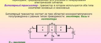
Bipolar transistors are essentially semiconductor devices. They are equipped with three pins and two pn junctions. The operating principle of these devices involves the use of positive and negative charges - holes and electrons. Flowing currents are controlled using a specially dedicated control current. These devices are widely used in electronic and radio engineering circuits.
In different types of transistors, holes and electrons - carriers of electricity - can have their own functions. The most common type is p-p-p due to the best parameters and technical characteristics. The leading role in such devices is played by electrons, which perform the main tasks of ensuring all electrical processes. They are approximately 2-3 times more mobile than holes, and therefore have increased activity. Qualitative improvements in devices also occur due to the collector junction area, which is significantly larger than the emitter junction area.
Each bipolar transistor has two pn junctions. When testing a transistor with a multimeter, this allows you to check the performance of the devices by monitoring the resistance values of the transitions when direct and reverse voltages are connected to them. For normal operation of the p-p-p-device, a positive voltage is applied to the collector, under the influence of which the base junction opens. After the base current occurs, the collector current appears. When a negative voltage occurs in the base, the transistor closes and the current flow stops.
The base junction in pnp devices opens when exposed to negative collector voltage. Positive voltage causes the transistor to turn off. All the necessary collector characteristics at the output can be obtained by smoothly changing the current and voltage values. This allows you to effectively test the bipolar transistor with a tester.
These devices are represented by modifications of the “p” or “p”-channel type. Channels can be located vertically or horizontally, and their configuration can be volumetric or near-surface. The latter option is also divided into inversion layers containing enriched and depleted ones. The formation of all channels occurs under the influence of an external electric field. Devices with near-surface channels have a metal-dielectric-semiconductor structure, which is why they are called MOS transistors.
Checking devices in the circuit
How to test a transistor with a multimeter without desoldering it, how to test a field-effect transistor - these questions arise among radio amateurs quite often. Removing a semiconductor device from a circuit requires great care and experience. It is necessary to have in your arsenal a low-voltage soldering iron with a thin tip and a bracelet that protects against static discharges. The conductors of the printed circuit board can overheat during operation, or even accidentally short-circuit with each other.
Although, if you have experience in such work, the task is completely solvable. Of course, you need to be able to read electrical diagrams and imagine the operation of each of its components.
Assessing the performance of low- and medium-power bipolar transistors differs little from checking these elements “on the table”, when all the terminals of the device are in a position accessible for testing.
It is more difficult to check directly in the circuit of high-power devices used in the circuits of output stages of amplifiers and switching power supplies. These circuits contain elements that protect transistors from reaching the maximum permissible modes. When checking the states of “p - n” transitions in these cases, you can get absolutely incorrect results. The solution is to solder the base output.
Checking field devices can give results that are far from the real state of affairs. The reason is the presence in the circuits of a large number of elements for correcting the operation of transistors, including low-resistance inductors.
There are still a large number of different types of transistors, to assess the condition of which it is necessary to use various special probes. But this is a topic for a separate article.
Instructions for checking with a tester
Testers differ by type of model:
- There are devices that are designed with devices that allow you to measure the gain of low-power microtransistors.
- Conventional testers allow testing in ohmmeter mode.
- The digital tester measures the transistor in diode test mode.
In any case, there is a standard instruction:
- Before starting the test, it is necessary to remove the charge from the bolt. This is done like this: literally for a few seconds the charge must be short-circuited with the source.
- In the case when a low-power field-effect transistor is being tested, then before picking it up, you must remove the static charge from your hands. This can be done by holding your hand on something metal that has a ground connection.
- When checking with a standard tester, you must first determine the resistance between drain and source. In both directions it should not make much difference. The resistance value with a working transistor will be small.
- The next step is to measure the junction resistance, first direct, then reverse. To do this, you need to connect the tester probes to the gate and drain, and then to the gate and source. If the resistance in both directions is different, the triode device is working properly.
A little about the design
The field effect transistor consists of the following elements:
- n-channel, which has a silicon substrate with p-conductivity;
- n-regions, which are obtained by adding impurities to the substrate;
- insulating the gate from the dielectric channel.
Pins are connected to n-areas. Current flows from source to drain through the transistor thanks to the power supply. The amount of current is controlled by the insulated gate of the transistor.
When working with a transistor component, you must consider its sensitivity to the effects of an electric field . Such elements should be stored with the terminals short-circuited with foil, and before soldering they will need to be short-circuited with wire. Soldering of transistor elements is carried out using a soldering station that provides protection against static electricity.
Before deciding how to test a mosfet with a multimeter, you need to determine its pinout. The imported device has marks corresponding to the terminals of the transistor. In this case, the letter G denotes the gate of the device, S is the source, and the designation D refers to the drain.
How to test a transistor without a multimeter
Testing a transistor without using a multimeter is not always possible. The use of light bulbs and power supplies in measurements can with a high probability damage the element being tested.
Checking a bipolar transistor can be done with a simple test using a 4.5 V battery, the negative of which is connected to a light bulb from a flashlight. Connect the “plus” and the second contact of the lamp to the terminals in pairs. If, when connected in any polarity to the “K-E” pair, the lamp does not light up, the transition is working. Connect through a limiting resistor “plus” to “B”. We alternately connect the lamp to terminals “E” or “K” and check these transitions. To test a transistor of a different structure, we change the polarity of the connection.
To test transistors, it is effective to use hand-made devices whose circuits are fairly accessible.
Simple transistor probes without desoldering from the circuit
There are many different circuits for testing transistors and measuring their parameters.
But in practice, most often you just need to quickly make sure that the transistor in the circuit is working, without going into the intricacies of its current-voltage characteristics. Below are two simple diagrams of such probes. They have a minimum of parts and do not require any special adjustment. At the same time, with their help you can easily and quickly test almost any transistor (except field-effect ones), both low-power and high-power, without removing it from the circuit. Also, using these circuits, you can experimentally determine the pinout of the transistor, the location of its terminals, if the transistor is unknown to you and there is no reference information on it. The currents through the transistor being tested in these circuits are very small, so even if you “reverse the polarity,” you will not damage the transistor.
The first circuit is assembled using a low-power transformer Tr1 (this can be found in almost any old pocket or portable transistor receiver, for example, Neva, Chaika, Sokol).
Such transformers are called transition transformers and serve to match the amplification stages in the receiver. The secondary winding of the transformer (it has a middle terminal) must be reduced to 150 - 200 turns.
The meter can be assembled in a suitable small-sized housing. The Krona type battery is located in the housing and is connected through the appropriate connector. Switch S1 - type “P2-K” or any other with two groups of contacts for switching. A capacitor can be taken with a capacity of 0.01 to 0.1 µF, and the tonality of the sound will change. Measuring probes “e”, “b”, “k” are made from pieces of wire of different colors, and it is convenient to make sure that the first letter of the wire color matches the letter of the transistor output. For example: Red – “ Collector ”, White – “ Base ”, Emitter – any other color (because there is no color starting with the letter “E”!). You need to solder small pieces of copper wire to the ends of the wires as tips. The probe can be assembled by mounted mounting by soldering a resistor and capacitor directly to the contacts of the switch and transformer.
If the transistor being tested is in good working order in the telephone capsule connected to the second winding of the transformer, a sound will be heard. It is necessary to use a high-impedance sound emitter (such as "DEMSH", for example), since the volume of its sound is sufficient for good audibility at a distance, so it can be located in the device body, and not taken outside. Low-impedance headphones and speakers will bypass the secondary winding of the transformer and the device may not work. You can turn on a telephone capsule as an emitter (take it out of an old handset. Although a new one will also work). If there is no suitable sound emitter with high resistance at all, then you can use an LED by connecting it instead of a capsule through an additional resistance (select the resistance taking into account the output voltage on the transformer so that its brightness is sufficient), then if the transistor is working properly, the LED will light up.
The second probe circuit is transformerless. The device and principle of operation are similar to the previous diagram
I have been using a similar circuit for many years and is capable of testing any transistors. Transistors of the old MP-40 type were used as T1 and T2, which can be replaced with any of this series (MP-39, -40, -41, -42). These are germanium transistors, the opening current of which is noticeably lower than that of silicon ones (such as KT-361, KT-3107, etc.) and when testing transistors without desoldering them from the circuit, no problems arise (the effect on the active elements of the circuit being tested is minimal). It is quite possible that modern silicon transistors will be suitable, but I personally have not tested this option in practice.
Checking the built-in freewheeling diode
In almost any modern field-effect transistor, with the exception of special types, an internal “protection” diode is connected in parallel to the drain-source circuit. The presence of this diode inside the field device is due to the peculiarities of the technology for producing high-power transistors. Sometimes it interferes and is considered parasitic, but most field-effect transistors cannot do without it, as part of the integral structure of the electronic component.
Therefore, in a working field-effect transistor, this diode should also be working. In an n-channel field-effect transistor, this diode is connected with the cathode to the drain, and the anode to the source, and in a p-channel field-effect transistor, the anode is connected to the drain, and the cathode is connected to the source. Turn the multimeter into diode testing mode. If the field-effect transistor is n-channel, then attach the red probe of the multimeter to its source (source), and the black one to the drain (drain).
Transistors are one of the most widely used radioelements. Despite their reliability, they often fail due to irregularities in their operation. At the same time, searching for a faulty element due to the specific design of the field-effect transistor causes certain difficulties.
Typically the drain is in the middle and connected to the conductive substrate of the transistor, and the source is the right pin (check this in the datasheet). If the internal diode is working properly, the multimeter display will display a direct voltage drop across it - around 0.4-0.7 volts. If the position of the probes is now reversed, the device will show infinity. If everything is so, then the internal diode is working.
Measurement order.
Checking the drain-source circuit
The field effect transistor is controlled by the electric field of the gate. And if the gate-source capacitance is charged, then the conductivity in the drain-source direction will increase. So, if the transistor is n-channel, apply the black probe to the gate and the red one to the source, and after a second, reverse the orientation of the probes - red to the gate and black to the source. So we probably first discharged the shutter, and then charged it. The gate is usually on the left and the source is on the right.
Now move the red probe from the gate to the drain, and let the black probe remain at the source. If the transistor is working properly, then as soon as you move the red probe from the gate to the drain, the multimeter will show that there is a voltage drop at the drain - this means that the transistor has switched to a conducting state.
Now the red probe is on the source, and the black probe is on the gate (we discharge the gate with the opposite polarity), after which again the red probe is on the drain, and the black probe is on the source. The device should show infinity - the transistor has closed. For a p-channel field-effect transistor, the probes are simply swapped.
Checking the transistor without soldering.
If the device beeps
If at the drain-source testing stage the device beeps, this may be quite normal, because modern field-effect transistors have very low drain-source resistance when open. Alternatively, you can connect the gate to the source and in this position ring drain-source (for n-channel, red to drain, black to source), the device should show infinity.
The main thing is that there is no gate-source and drain-source ringing, especially at the moment when the gate is charged with the opposite polarity.
Instructions for dialing without soldering
To check whether the field-effect transistor is working, you need to unsolder it and test it with a multimeter. However, situations may arise when you need several such parts in the circuit and it is not known which of them are working and which are not. In this case, it is useful to know how to test a field-effect transistor with a multimeter without desoldering.
Digital multimeter
In this case, a test without desoldering is used. It gives an approximate result.
Important! After the presumably faulty element has been identified, it is disconnected and checked, obtaining accurate information about its performance. If it functions normally, it is installed in its original place.
Testing without desoldering is performed as follows:
- Before testing the field-effect transistor with a digital multimeter, disconnect the device from the electrical outlet or from the batteries. The latter are removed from the device.
- If the red probe is connected to the source, and the black probe to the drain, then you can expect that the multimeter will show 500 mV. If you can see this figure or one that exceeds it on the indicator, this indicates that the transistor is fully functional. If this value is much less - 50 or even 5 mV, then in this case a malfunction can be assumed with a high probability.
You might be interested in: Features of a two-zone meter
With control pn junction
- If the red multimeter probe is moved to the gate, and the black one is left in the same place, then the indicator will show 1000 mV or more, which indicates the serviceability of the field-effect transistor. When the difference is 50 mV, this raises concerns that the part is damaged.
- If the black probe of the tester is placed on the source, and the red probe is placed on the gate, then for a working transistor you can expect 100 mV or more on the display. In cases where the figure is less than 50 mV, there is a high probability that the part being tested is inoperative.
It must be taken into account that the conclusions obtained without soldering are probabilistic in nature. These data allow us to draw preliminary conclusions about the field-effect transistors used in the circuit.
To check, they need to be unsoldered, checked and installed if the functionality is confirmed.
Preparing for work
Bipolar
How to test a bipolar transistor with a multimeter? First of all, you need to find out which of the two subtypes - npn or pnp it belongs to. To do this, let’s remember what a bipolar transistor is.
This is a semiconductor element in which the so-called npn or pnp junction is implemented. Npn is the transition "electron - hole - electron", pnp, respectively, on the contrary, "hole - electron - hole".
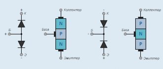
Structurally, it consists of three parts - emitter, collector and base. In fact, a bipolar is two conjugated ordinary diodes, in which the base is the common connection point.
In the pnp circuit, the transistor differs from its npn counterpart in the direction of the arrow in the circle - the arrow of the emitter junction. For a pnp circuit it is directed towards the base, for an npn circuit it is directed vice versa.
You need to know this difference to check the bipolar transistor. A Pnp circuit is opened by applying a negative voltage to the base, and an Npn one by applying a positive voltage. But before this, it is necessary to find out which of the contacts of the transistor being tested is the base, which is the emitter, and which is the collector.
The instructions here could be as follows:
- the red (positive) probe is connected to the first terminal that comes across, for example the left one, the black (negative) probe alternately touches the central and right ones. Fix the value “1” on the central one, and 816 Ohms, for example, on the right;
- The red probe of the multimeter is short-circuited with the central contact, the black one - alternately with the side ones. The device displays “1” on the left and some value, say 807, on the right;
- when the red probe of the multimeter contacts the right terminal, and the black probe contacts the left and center, we get “1” in both cases. This means that the base is defined - this is the right contact of the transistor. And the transistor itself is PNP type.
In principle, this is enough to say that the transistor is working. Now, to check its structure and the specific location of the emitter and collector, we short-circuit the black (negative) probe of the multimeter with the base, and the red one in turn with the left and center contacts.
The contact that gives a lower resistance value will be a collector contact (in our case, 807 Ohms). The larger one - 816 Ohms - is the emitter one.
Testing an NPN type transistor occurs in the same way, only the positive contact is applied to the base.
This is a way to test pn junctions between base and collector and base and emitter. The multimeter readings may vary depending on the type of transistor, but will always be within the range of 500-1200 Ohms.
To complete the test, touch the emitter and collector probes. A working element will produce infinitely high resistance, regardless of its type, no matter how you change the polarity. If the value on the screen differs from “1”, one of the transitions is broken, the part is unusable.
Checking the functionality of the field-effect transistor
This type of semiconductor elements is also called mosfet and mosfet components. Figure 4 shows the graphic designation of n- and p-channel field switches in circuit diagrams.
To test these devices, we connect the probes to the multimeter in the same way as when testing bipolar semiconductors, and set the test type to “continuity”. Next, we proceed according to the following algorithm (for an n-channel element):
- We touch the black wire to the “c” pin, and the red wire to the “i” pin. The resistance on the built-in diode will be displayed, remember the reading.
- Now you need to “open” the transition (this will only be possible partially), for this we connect the probe with the red wire to terminal “z”.
- We repeat the measurement carried out in step 1, the reading will change downwards, which indicates a partial “opening” of the field worker.
- Now you need to “close” the component, for this purpose we connect the negative probe (black wire) to the “z” leg.
- We repeat steps 1, the original value will be displayed, therefore, “closing” has occurred, which indicates the serviceability of the component.
To test p-channel elements, the sequence of actions remains the same, with the exception of the polarity of the probes, it must be reversed.
Note that insulated gate bipolar elements (IGBT) are tested in the same way as described above. Figure 5 shows the SC12850 component in this class.
Fig 5. IGBT transistor SC12850
For testing, it is necessary to perform the same steps as for a field-effect semiconductor element, taking into account that the drain and source of the latter will correspond to the collector and emitter.
In some cases, the potential on the multimeter probes may not be enough (for example, to “open” a powerful power transistor); in such a situation, additional power will be needed (12 volts will be enough). It must be connected through a resistance of 1500-2000 Ohms.
Expert opinion
Viktor Pavlovich Strebizh, lighting and electrical expert
Any questions ask me, I will help!
For bipolar PNP conductivity devices, the open state will correspond to the connection of the negative black probe of the tester to the base terminal. If there is something you don’t understand, write to me!
Where to begin?
Before checking any element with a multimeter for serviceability, be it a transistor, thyristor, capacitor or resistor, it is necessary to determine its type and characteristics. This can be done by marking. Once you know it, it won’t be difficult to find a technical description (datasheet) on thematic sites. With its help, we will find out the type, pinout, main characteristics and other useful information, including replacement analogues.
For example, the scanning on the TV stopped working. Suspicion is raised by the line transistor marked D2499 (by the way, a fairly common case). Having found a specification on the Internet (a fragment of it is shown in Figure 2), we receive all the information necessary for testing.
Figure 2. Specification fragment for 2SD2499
There is a high probability that the datasheet found will be in English, no problem, the technical text is easy to understand even without knowledge of the language.
Having determined the type and pinout, we solder the part and begin testing. Below are the instructions with which we will test the most common semiconductor elements.
Main causes of malfunction
The most common reasons for a triode element in an electronic circuit to fail to operate are as follows:
- Break in the transition between components.
- Breakdown of one of the transitions.
- Breakdown of the collector or emitter section.
- Power leakage under voltage.
- Visible damage to the terminals.
Characteristic external signs of such a breakdown are blackening of the part, swelling, and the appearance of a black spot. Since these shell changes occur only with high-power transistors, the issue of diagnosing low-power ones remains relevant.
Source
Checking the bipolar transistor
This procedure for bipolar transistors begins with proper setup of the device. The device is switched to semiconductor testing mode; one should appear on the display. The terminals are connected in a similar way to the resistance measurement mode. A black wire is connected to the COM port, and a red wire is connected to the output to measure voltage, resistance and frequency. If the multimeter does not have a corresponding mode, then the process should be carried out in resistance measurement mode when set to maximum.
It is also important that the multimeter battery is fully charged and the probes are in good working order. When connecting the tips, serviceability is indicated by the squeak of the device and zeros on the screen
The procedure in this case follows the following steps:
- We correctly connect the leads of the multimeter and the transistor. We determine the location of the base, collector and emitter. The probes are swapped until the voltage drops. We check using base-emitter or base-collector pairs.
- The base-collector pair means that the red probe is connected to the base, and the black probe is connected to the collector. The connection operates in diode mode and conducts current in only one direction.
- When testing through a base-emitter connection, the black wire is connected to the emitter. The current also flows exclusively in the forward direction.
- The emitter-collector junction is operational if the resistance on the screen tends to infinity.
- We connect the multimeter to each pair of contacts in both directions in the opposite direction, connect the black probe to the base. The results obtained are compared.
- The functionality of the device is confirmed by the presence of finite resistance; reverse polarity shows one.
As a result, there is no need to solder the element to ensure its serviceability. If you want to use light bulbs and other elements to test, it is not recommended to do this, since there is a risk of permanently damaging the bipolar transistor.
Checking digital transistors
A digital transistor is no different in appearance from a regular one, but the results of its “diagnosis” can confuse even an experienced technician. For many they were “incomprehensible” and remain so. In some articles you can find the statement - “testing digital transistors is difficult.
The best option is to replace it with a known-good transistor.” Undoubtedly, this is the most reliable method of verification. Let's try to figure out if this is really so. Let's figure out how to properly test a digital transistor and what conclusions to draw from the measurement results.
In the forward direction, the base-collector circuit of the transistor in question consists of a series-connected resistor R1 and the resistance of the base-collector junction itself. The junction resistance, since it is significantly less than the resistance of resistor R1, can be neglected.
This measurement will give a value approximately equal to the resistance value of resistor R1, which in our example is 10 kOhm. In the opposite direction, the junction remains closed and no current flows through this resistor. The avometer needle should show “infinity”.
The base-emitter circuit is a mixed connection of resistors R1, R2 and the resistance of the base-emitter junction itself (VD2 in Fig. 4 on the left). Resistor R2 is connected in parallel to this junction and practically does not change its resistance.
Therefore, in the forward direction, when the junction is open, the ampere-volt-ohmmeter will again show a resistance value approximately equal to the resistance value of the base resistor R1. When the polarity of the tester is changed, the base-emitter junction remains closed. Current flows through resistors R1 and R2 connected in series. In this case, the tester will show the sum of these resistances. In our example it will be approximately 32 kOhm.
As you can see, in the forward direction, a digital transistor is tested in the same way as a conventional bipolar transistor. The difference is that the arrow of the device shows the resistance value of the base resistor.
From the difference in the measured resistances in the forward and reverse directions, you can determine the resistance value of resistor R2.
Now let's look at testing the emitter-collector circuit. This circuit consists of two back-to-back diodes, and with any polarity of the tester, its arrow should show “infinity”. However, this statement is only true for a conventional silicon transistor.
In the case under consideration, due to the fact that the base-emitter junction (VD2) turns out to be shunted by resistor R2, it becomes possible to open the base-collector junction with the corresponding polarity of the measuring device. The transistor resistance measured in this case has some scatter, but for a preliminary assessment you can focus on a value that is approximately 10 times less than the resistance of resistor R1.
When changing the polarity of the tester, the resistance of the base-collector junction should be infinitely large. For a direct conduction transistor, the arrow will indicate “-” on the measuring device. As a measuring device, it is necessary to use pointer (analog) AVOmeters with a head deflection current of about 50 μA (20 kOhm/V).
Multifunction tester.
It should be noted that the above is somewhat idealized, and in practice, there may be situations that require logical interpretation of the measurement results. Especially in cases where the digital transistor turns out to be defective.
How to solder field-effect transistors correctly and safely: 5 tips
I recommend that beginners pay close attention to this issue. Then you will not be disappointed with the work done.
Where is the ambush hidden or why is static dangerous for electronics?
In everyday life, we rarely feel static electricity, for example, when combing our hair with a plastic comb, getting out of the car after a trip, or in some other cases.
Usually, static causes minor troubles to our body that are simply annoying. But with semiconductors things are different.
MOSFETs have a very thin layer of insulation between the gate and the channel material. It forms a capacitive coupling between gate-source and gate-drain. Moreover, the dielectric itself creates this effect, working as a capacitance.
We know that any capacitor is manufactured to operate at a certain voltage. If it is exceeded, an insulation breakdown occurs. Ten volts are usually enough to damage the oxide film of the field grass, and sometimes less.
Now I’m showing with photographs what dangers we can create for transistors with our own hands if we don’t follow the rules for soldering them.
I took my favorite Moment transformer soldering iron, plugged its power cord into the outlet, but did not press the power button. I placed one end of the multimeter wire through an alligator clip onto the sting, and the other just leaned it against my finger. Set the AC voltmeter mode.
The device shows 28 volts. This is the kind of interference that is created even when the transformer is de-energized.
I continue the experiment. I left the black probe in the same place, and leaned the red one against the dielectric surface of the stool, where all the instruments are located.
Almost 6.4 volts. When I separated the red probe with air space, the reading became 8 volts.
But these are completely random measurements, the results of which depend on many factors, which means: the voltage can be significantly more or less.
We may not even feel this static, but its random discharge can burn out the thin semiconductor junction of the crystal.
To prevent this, it is important to follow the mandatory recommendations.
How to avoid hidden dangers and work safely with a soldering iron: 5 recommendations
Tip #1: Bypassing the leads
Damage to semiconductor junctions during storage and operation can be prevented by keeping microcircuits, transistors, and integrated electronics products in a layer of foil.
A similar result, in particular, is obtained if you wrap the contacts of their terminals with thin copper wire without insulation.
Tip #2: removing static from operating equipment
It is best to work with a professional soldering station with a grounded tip. If it is not there, then ground the soldering iron tip and the circuit board with separate conductors. Shunt the transistor leads with a thin wire, which will be removed after soldering.
A grounding bracelet on your hand or other part of the body allows you to remove the dangerous potential of static from tweezers and the tool you will be working with. Its 1 MΩ resistance eliminates the possibility of dangerous static discharge.
Tip No. 3: preparing the workplace
The dry air of northern latitudes, especially in winter, contributes to the accumulation of static on surrounding objects. Humidifiers and air washes successfully combat this phenomenon.
An antistatic mat immediately and reliably removes static potentials and the effects of electrical noise from the environment.
Tip #4: professional mixtures
A special flux of the FluxOff brand not only perfectly washes away rosin and traces of corrosion, but actually removes static. They just need to wet the board.
Tip #5: Quick soldering
Choose the minimum required soldering iron power, but work quickly with it. Experienced repairmen manage to heat up the tip, take solder with it, turn off the power to the soldering iron and then solder the part in place.
Some modern microcircuits and transistors are protected against static, but this does not eliminate the need to follow the rules of safe soldering with all other products.
How a field-effect transistor works: 6 types - brief information
The classification shown in the picture below, where their types are structured, will help us deal with a specific field grass and understand its structure.
JFET and MOSFET have different structure. In JFET, the gate (Gate) is directly built into the cross section of the channel and works as a control pn junction.
For mosfet:
- there is an additional fourth pin connected internally to the housing. It is not used when connecting to external circuits;
- The gate output region is separated by a layer of silicon dioxide (dielectric) from the channel semiconductor. It works as a plate capacitively coupled capacitor. Due to this modification, it is called an “insulated gate” or MOS transistor.
MIS stands for metal-dielectric-semiconductor and MOS stands for metal-oxide-semiconductor. The difference between them for a novice electrician is not significant, practically absent.
In the diagrams, mosfet and jifet are designated in different ways. MOSFET is drawn with:
- the fourth pin, which is not connected anywhere;
- a shutter separated from the main channel.
Mosfets are manufactured with different substrates (channels), which can be depleted or enriched in major charge carriers.
I will not describe and describe in more detail the differences between each type of these semiconductors for a novice electrician: there is not much point.
Below are just typical schedules of their work. They will give a general idea of behavior, and you will need to take specific data from the datasheet - technical documentation.
The amount of current flowing through the drain depends on the applied voltage between gate and source, as well as the ambient temperature.
The output drain current characteristics depend on the magnitude of the applied voltage between drain-source and gate-source.
This is how a MOS transistor with a built-in channel works. The current slope increases with increasing voltage Usi, Uzi.
And here are the characteristics of transistors with an induced channel.
Before any check of each transistor, it is necessary to clarify its technical capabilities according to the factory documentation.
Such graphical images and dependencies of electrical engineering processes, due to their clarity, have better information content.
6 features of electronic devices using MOSFETs
Recently, we are increasingly working with mosfet-type field devices with a channel of any conductivity.
Let us briefly analyze such a scheme and its properties.
Point No. 1: which shoulder to place the load on?
When the semiconductor junction is completely open, a very small resistance of tens or hundreds of milliOhms (Ropen) is created between the drain and the source, which forms a low voltage drop in this section (In · Roopen), where In is the value of the load current.
The voltage potential applied to the gate may not be sufficient to fully open the semiconductor. Therefore, the load is turned on higher on the drain side in an n-type field switch, and on the source side in a p-type field switch when the circuit is powered from a single source.
If the device uses additional voltage sources, then this requirement is not necessary.
Point No. 2: tricks for connecting a field worker to microcontrollers
For reliable operation of the MOSFET, it is necessary to apply a threshold voltage value between its gate and source (gate-source), which is indicated in the datasheet. It is usually around 10 volts. Still, digital devices work up to five: their power supply is not enough, you will need to add a level.
You can solve the problem in one of three ways:
- a key with bipolar transistors supplies the necessary power to the gate;
- connect a special driver (chip) to generate a control signal. They are designed for both the upper and lower shoulder to accommodate the load. Moreover, the high-side driver often uses a circuit to increase the output voltage;
- use a specialized low-level field operator (logic level). However, acquiring it can be problematic.
Point No. 3: how to avoid the influence of electrical interference
The appearance of any interference potential at the output of a transistor often leads to its unauthorized switching and disruption of electronic operating algorithms.
Therefore, the gate is always “pulled” to power or ground through a certain resistance, even when connected through a microcontroller. It should not be left in a free state, accessible to the penetration of extraneous interference.
Point No. 4: combating surge current when turned on
The natural presence of capacitance at the gate pin leads to a “current surge” each time the transistor is turned on. This can lead to damage to the semiconductor junction.
The problem is solved by introducing a resistor of sufficient value into the gate circuit. However, its value must be selected taking into account the increase in the key opening time.
Feature No. 5: inrush current protection when disconnecting inductive loads
A protective high-speed TVS diode, connected in parallel between the source and drain, reliably shunts the pulses created by disconnecting inductive loads.
When operating at high frequencies in bridge or half-bridge circuits of switching power supplies or induction heaters of hobs, a Schottky diode is connected counter-currently to the drain output, blocking the parasitic diode, because it increases the closing time, which can damage the semiconductor.
Point No. 6: additional MOSFET
Safe operation of a high-speed high-frequency switch in the switching mode of powerful inductive loads is ensured by its connection to snubber circuits. They:
- aperiodic currents created by transient processes close on themselves;
- reduce heating of semiconductors;
- protect the field switch from unauthorized opening during a rapid increase in voltage between drain and source.
Device diagram
The probe designer consists of only 7 electronic components + printed circuit board. It assembles quickly and starts working absolutely without any setup.
The circuit is assembled on a K155LN1 containing six inverters. When the leads of a working transistor are correctly connected to it, one of the LEDs lights up (HL1 with an NPN structure and HL2 with a PNP structure). If faulty:
- broken, both LEDs flash
- has an internal break, both do not ignite
The diodes being tested are connected to terminals “K” and “E”. Depending on the polarity of the connection, HL1 or HL2 will light up.
There are not many components of the circuit, but it is better to make a printed circuit board; it is troublesome to solder the wires to the legs of the microcircuit directly.
And try not to forget to put a socket under the chip.
You can use the probe without installing it in the case, but if you spend a little more time on its manufacture, you will have a full-fledged, mobile probe that you can already take with you (for example, to the radio market). The case in the photo is made from the plastic case of a square battery, which has already served its purpose. All that was needed was to remove the previous contents and saw off the excess, drill holes for the LEDs and glue a strip with connectors for connecting the transistors being tested. It would be a good idea to “dress” the connectors with identification colors. A power button is required. The power supply is a AAA battery compartment screwed to the case with several screws.
The fastening screws are small in size, it is convenient to pass them through the positive contacts and tighten them with the obligatory use of nuts.
The tester is in full readiness. It would be optimal to use AAA batteries; four 1.2 volt batteries will give the best supply voltage of 4.8 volts.
For complete convenience, crocodile extension cords are desirable. Then certainly not a single transistor will accidentally fall out and is guaranteed not to be lost, especially important when using the tester in “field” conditions.