Good day everyone, in today’s article we will begin a discussion of a very important and extensive topic dedicated to transistors. We will analyze the theoretical aspects, structure, types, consider the principle of operation using practical examples, the methodology for calculating circuits, in general, we will try to touch on it as much as possible.
To make the discussion as structured and understandable as possible, the material will be divided into clear sections and different articles. And, since transistors can immediately be divided into two large classes, namely bipolar and field-effect , then we’ll do just that - we’ll start with a detailed analysis of bipolar ones and, having studied them completely, we’ll move on to field ones.
What is a bipolar transistor
Transistors can be thought of as switches of sorts, just like many electronic components such as relays or vacuum tubes.
Transistors are used in various circuits, and rarely is a circuit complete without them, even now with the widespread use of microcircuits. There are two main types of bipolar transistors - npn and pnp, they differ in conductivity. Two similar transistors of different conductivities are called a complementary pair. If in some circuit, for example, in an amplifier, you replace transistors of one type with transistors of another type with similar parameters (not forgetting to change the polarity of the supply voltages, electrolytic capacitors and semiconductor diodes), then the circuit will work exactly the same, with the exception Microwave range, since npn transistors are higher frequency than pnp, and here it may not be possible to select a complementary pair.
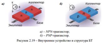
A bipolar transistor is a three-electrode semiconductor device, a type of transistor. The electrodes are connected to three successively arranged semiconductor layers with alternating types of impurity conductivity.
Most often, transistors of the NPN structure are used in circuits. This is due to the fact that in the circuits the emitters of the transistors are connected to a negative power supply.
Accordingly, the common wire of the circuit will also be connected to the negative terminal of the power supply, which is a generally accepted standard.
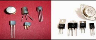
Transistors are available in various cases, but they all have three terminals (high-frequency transistors sometimes have a fourth terminal connected to a metal case - a screen):
- The base is the control output;
- The collector is under positive potential (for an NPN transistor);
- The emitter is at negative potential (for an NPN transistor).
NPN transistor operation:
Now that the n side of the diode has the most electrons and the p side has the most holes, all voltage connections are arranged as forward and reverse bias respectively. The emitter base junction is configured as reverse bias and the collector base junction is configured as forward bias. The depletion region of this emitter-base region is narrower compared to the depletion region at the collector-base intersection.
Since the junction is reverse biased (emitter), the holes flow from the power supply to the N junction. The electron then moves towards p. Here some electron is neutralized. The remaining electrons move towards n. The voltage drop relative to the emitter and base is VBE as the input side.
In N-type emitters, the charge carriers are mainly electrons. Consequently, electrons are transferred through the N-type emitters to the P-type base. The current will flow through the emitter-base or EB junction. This current is known as emitter current (Ie). Here, the emitter current (IE) flows from the output side and flows in two directions; one is IB and the other is IC. So we can write:
It will be interesting➡ What is a phase, how to determine phase and zero in electricity
IE=IB+IC
However, the base region is relatively thin and lightly doped. Consequently, most of the electrons pass through the base region and only a few of them recombine with the available holes. The base current is minimal compared to the emitter current. Typically this is up to 5% of the total emitter current.
The current flowing from the rest of the electrons is called collector current (IC). YC is relatively high compared to baseline (IB).
Bipolar transistor device
According to standard circuits, the letter “B” is called “Base” - the inner layer of the device, its foundation, which leads to the conversion or change of the current signal. The arrow in the circle shows the movement of current charges in “E”.
“E” - “Emitter” - the internal main component of the transistor, designed to transfer charged elementary particles to “B”.
“K” - “Collector” is the second component of the transistor device, which collects the same charges that pass through “B”.
The “Base” layer is structurally very thin due to the recombination of charged particles that go through the base layer with the constituent particles of this layer. At the same time, the “Collector” layer is designed as wide as possible for high-quality collection of charges.
How to choose a MOSFET transistor
The example above uses an N-channel FET. P-channel FETs work the same way, only the current flows in the opposite direction and the gate-source voltage must be negative.
There are thousands of different FETs to choose from. But if you want to build the circuit above, then you can use BS170 or IRF510.
There are two things to consider when choosing a field effect transistor:
- Gate-source threshold voltage. A higher voltage is required to turn on the transistor.
- Continuous drain current. This is the maximum current that can flow through the transistor.
There are other important parameters to keep in mind, depending on the application. But this is beyond the scope of this article. Keep these two parameters in mind and you'll have a good starting point.
Types of bipolar transistors
Bipolar transistors are classified into the following types: 1. Based on the source material - germanium or silicon. 2. According to production technology - alloy, epitaxial-planar, conversion, etc. 3. According to the mechanism of movement of charge carriers - drift and diffusion. 4. By power dissipation - low power (up to 0.3 W), medium power (from 0.3 to 3 W) and high power (more than 3 W). 5. According to the range of operating frequencies - low frequency (up to 3 MHz), medium (from 3 to 30 MHz), high (from 30 to 300 MHz), ultra-high frequency (more than 300 MHz).
Features of the transistor device
The NPN transistor includes three regions:
- emitter;
- the base is very thin, which is made of a lightly doped semiconductor, the resistance of this area is high;
- collector - its area is larger in size than the emitter area.
Metal contacts are soldered to each area, which serve to connect the device to the electrical circuit.
The collector and emitter conductivities are the same and opposite to the base conductivities. In accordance with the type of conductivity of the areas, pnp or npn devices are distinguished. The devices are asymmetrical due to the difference in contact area - between the emitter and base it is much lower than between the base and collector. Therefore, it is impossible to swap K and E by changing polarity.
The principle of operation of a bipolar transistor
Now we will try to figure out how a transistor works. I will not go into details of the internal structure of transistors as this information will only confuse. Better take a look at this drawing.
This image best explains the working principle of a transistor. In this image, a person controls the collector current using a rheostat. He looks at the base current; if the base current increases, then the person also increases the collector current, taking into account the gain of the transistor h21E. If the base current drops, then the collector current will also decrease - the person will correct it using a rheostat.
This analogy has nothing to do with the actual operation of a transistor, but it makes it easier to understand the principles of its operation.
For transistors, rules can be noted to help make things easier to understand. (These rules are taken from the book “The Art of Circuit Design” by P. Horowitz W. Hill).
- The collector has a more positive potential than the emitter
- As I already said, the base-collector and base-emitter circuits work like diodes
- Each transistor is characterized by limiting values such as collector current, base current and collector-emitter voltage.
- If rules 1-3 are followed, then the collector current Ik is directly proportional to the base current Ib. This relationship can be written as a formula.
From this formula we can express the main property of a transistor - a small base current controls a large collector current.
- current gain.
It is also denoted as
Based on the above, the transistor can operate in four modes:
- Transistor cutoff mode - in this mode, the base-emitter junction is closed, this can happen when the base-emitter voltage is insufficient. As a result, there is no base current and therefore there will be no collector current either.
- The active mode of a transistor is the normal mode of operation of the transistor. In this mode, the base-emitter voltage is sufficient to cause the base-emitter junction to open. The base current is sufficient and the collector current is also available. The collector current is equal to the base current multiplied by the gain.
- Transistor saturation mode - the transistor enters this mode when the base current becomes so large that the power of the power source is simply not enough to further increase the collector current. In this mode, the collector current cannot increase following an increase in the base current.
- Inverse transistor mode - this mode is used extremely rarely. In this mode, the collector and emitter of the transistor are swapped. As a result of such manipulations, the gain of the transistor suffers greatly. The transistor was not originally designed to operate in such a special mode.
To understand how a transistor works, you need to look at specific circuit examples, so let's look at some of them.
Transistor in switch mode
A transistor in switch mode is one of the cases of transistor circuits with a common emitter. The transistor circuit in switching mode is used very often. This transistor circuit is used, for example, when it is necessary to control a powerful load using a microcontroller. The controller leg is not capable of pulling a powerful load, but the transistor can. It turns out that the controller controls the transistor, and the transistor controls a powerful load. Well, first things first.
The main idea of this mode is that the base current controls the collector current. Moreover, the collector current is much greater than the base current. Here you can see with the naked eye that the current signal is amplified. This amplification is carried out using the energy of the power source.
Recommended reading: Stepper motor control
The figure shows a diagram of the operation of a transistor in switching mode.
For transistor circuits, voltages do not play a big role, only currents matter. Therefore, if the ratio of the collector current to the base current is less than the gain of the transistor, then everything is okay.
In this case, even if we have a voltage of 5 volts applied to the base and 500 volts in the collector circuit, then nothing bad will happen, the transistor will obediently switch the high-voltage load.
The main thing is that these voltages do not exceed the limit values for a specific transistor (set in the transistor characteristics).
Well, now let's try to calculate the value of the base resistor.
As far as we know, the current value is a characteristic of the load.
Those. I=U/R
We don't know the resistance of the light bulb, but we know the operating current of the light bulb is 100 mA. In order for the transistor to open and allow such current to flow, you need to select the appropriate base current. We can adjust the base current by changing the value of the base resistor.
Since the minimum value of the transistor gain is 10, then for the transistor to open, the base current must become 10 mA.
The current we need is known. The voltage across the base resistor will be This voltage value across the resistor is due to the fact that 0.6V-0.7V is dropped at the base-emitter junction and we must not forget to take this into account.
As a result, we can easily find the resistance of the resistor
All that remains is to choose a specific value from a number of resistors and it’s done.
Now you probably think that the transistor switch will work as it should? That when the base resistor is connected to +5 V the light bulb lights up, when it is turned off the light bulb goes out? The answer may or may not be yes.
The thing is that there is a small nuance here.
The light bulb will go out when the resistor potential is equal to the ground potential. If the resistor is simply disconnected from the voltage source, then everything is not so simple. The voltage on the base resistor can miraculously arise as a result of interference or some other otherworldly evil spirit
To prevent this effect from happening, do the following. Another resistor Rbe is connected between the base and emitter. This resistor is chosen with a value at least 10 times larger than the base resistor Rb (In our case, we took a 4.3 kOhm resistor).
When the base is connected to any voltage, the transistor works as it should, the resistor Rbe does not interfere with it. This resistor consumes only a small portion of the base current.
In the case when voltage is not applied to the base, the base is pulled up to the ground potential, which saves us from all kinds of interference.
So, in principle, we have figured out the operation of the transistor in the key mode, and as you can see, the key mode of operation is a kind of voltage amplification of the signal. After all, we controlled a voltage of 12 V using a low voltage of 5V.
Emitter follower
An emitter follower is a special case of common-collector transistor circuits.
A distinctive feature of a circuit with a common collector from a circuit with a common emitter (option with a transistor switch) is that this circuit does not amplify the voltage signal. What went in through the base came out through the emitter, with the same voltage.
Indeed, let’s say we applied 10 volts to the base, while we know that at the base-emitter junction somewhere around 0.6-0.7V is dropped. It turns out that at the output (at the emitter, at the load Rн) there will be a base voltage of minus 0.6V.
It turned out 9.4V, in a word, almost as much as went in and out. We made sure that this circuit will not increase the voltage for us.
“What is the point then of turning on the transistor like this?” you ask. But it turns out that this scheme has another very important property. The circuit for connecting a transistor with a common collector amplifies the signal in terms of power. Power is the product of current and voltage, but since the voltage does not change, the power increases only due to the current! The load current is the sum of the base current plus the collector current. But if you compare the base current and the collector current, the base current is very small compared to the collector current. It turns out that the load current is equal to the collector current. And the result is this formula.
Now I think it’s clear what the essence of the emitter follower circuit is, but that’s not all.
The emitter follower has another very valuable quality - high input impedance. This means that this transistor circuit consumes almost no input current and creates no load on the signal source circuit.
To understand the principle of operation of a transistor, these two transistor circuits will be quite sufficient. And if you experiment with a soldering iron in your hands, the epiphany simply won’t keep you waiting, because theory is theory, and practice and personal experience are hundreds of times more valuable!
Why do you need a transistor?
I often have a question: why do we need a transistor? Why not connect the LED and resistor directly to the battery?
The advantage of a transistor is that you can use a small current or voltage to control a much larger current and voltage.
This is very useful if you want to control things like motors, high power LEDs, speakers, relays and more using a microcontroller/Raspberry Pi/Arduino. The output of the microcontroller can only provide a few milliamps at 5V. So if you want to control, for example, a 230V street light, you cannot do it directly with the microcontroller
You can use a relay instead. But even a relay usually requires more current than the microcontroller output can provide. Therefore you will need a transistor to drive the relay:
It will be interesting➡ What is automatic reserve entry and how does ATS work? Basic ATS schemes and their features.
Advantages and disadvantages of bipolar transistors
The advantages of bipolar transistors in comparison with analogues include:
- control of electrical charges;
- reliability in operation;
- resistance to frequency interference;
- low noise characteristics;
The disadvantages include:
- has a low input resistance, due to which the signal amplification characteristics deteriorate;
- severe sensitivity to static charges;
- the connection diagram assumes the presence of 2 power supplies;
- At high temperatures the transistor may be damaged.
Content
- 1 Operating principle of a transistor
- 2 Operating modes of a bipolar transistor 2.1 Normal active mode
- 2.2 Inverse active mode
- 2.3 Saturation mode
- 2.4 Cut-off mode
- 3.1 Connection diagram with a common base
How to test a bipolar transistor
Since a bipolar transistor consists of two pn junctions, checking it with a digital tester is quite simple.
It is necessary to set the tester operation switch to the diode test position, connecting one probe to the base, and the second - alternately to the emitter and collector.
Essentially, we are simply sequentially checking the health of the pn junctions.
Such a transition can be either open or closed.
Then you need to change the polarity of the probes and repeat the measurements.
In one case, the tester will show a voltage drop at the emitter-base and collector-base junctions of 0.6 - 0.7 V (both junctions are open).
In the second case, both transitions will be closed, and the tester will record this.
It should be noted that in operating mode, most often one of the transitions of the transistor is open and the second is closed.
Let's look at the differences between the PNP type in the connection diagram with a common base
Indeed, it can be seen that the collector current IC (in the case of an NPN transistor) flows from the positive terminal of battery B2, passes through the collector terminal, penetrates into it and must then exit through the base terminal to return to the negative terminal of the battery. In the same way, looking at the emitter circuit, you can see how its current from the positive terminal of battery B1 enters the transistor through the base terminal and then penetrates into the emitter.
The base terminal thus carries both the collector current IC and the emitter current IE. Since they circulate in opposite directions along their circuits, the resulting base current is equal to their difference and is very small, since IC is slightly smaller than IE. But since the latter is still larger, the direction of flow of the difference current (base current) coincides with IE, and therefore a PNP-type bipolar transistor has a current flowing out of the base, and an NPN-type one has an inflowing current.
Measuring the current gain of a bipolar transistor
If the tester has the ability to measure the current transfer coefficient, then you can check the operation of the transistor by installing the transistor leads into the corresponding sockets.
We recommend reading: Varistor: principle of operation, main characteristics, designation on the diagram
Current transfer coefficient is the ratio of the collector current to the base current.
The higher the gain, the more collector current can be controlled by the base current, all other things being equal.
The pinout (pin name) and other data can be taken from the data sheets (reference data) for the corresponding transistor. Data sheets can be found on the Internet through search engines.
The tester will show on the display the current transfer (gain) coefficient, which must be compared with the reference data.
The current transfer coefficient of low-power transistors can reach several hundred.
For powerful transistors it is significantly smaller - several units or tens.
However, there are powerful transistors with a transfer coefficient of several hundred or thousand. These are the so-called Darlington pairs.
A Darlington pair consists of two transistors. The output current of the first transistor is the input current for the second.
The overall current transfer coefficient is the product of the coefficients of the first and second transistors.
The Darlington pair is made in a common housing, but it can also be made from two separate transistors.
Applications of PNP transistors:
- PNP transistors are used as switches i.e. analog switches, emergency buttons, etc. They are used when emergency shutdown is required.
- These types of transistors are used in current source circuits, i.e., by taking advantage of the characteristics of the current flowing from the collector.
- Used in amplification circuits.
- They are used in paired Darlington circuits.
- PNP transistors are used in heavy-duty motors for current control and in various robot and microcontroller development applications.
Next
MiscellaneousWhat is active power?
Built-in diode protection
Some transistors (power and high voltage) can be protected from reverse voltage by a built-in diode.
Thus, if you connect the tester probes to the emitter and collector in diode testing mode, it will show the same 0.6 - 0.7 V (if the diode is forward biased) or a “blocked diode” (if the diode is reverse biased) .
If the tester shows some small voltage, and in both directions, then the transistor is definitely broken and must be replaced. A short can also be determined in resistance measurement mode - the tester will show low resistance.
There is (fortunately, quite rarely) a “mean” malfunction of transistors. This is when it works at first, but after some time (or after warming up) it changes its parameters or fails altogether.
If you unsolder such a transistor and check it with a tester, it will have time to cool before the probes are connected, and the tester will show that it is normal. The best way to verify this is by replacing the “suspicious” transistor in the device.
In conclusion, let’s say that the bipolar transistor is one of the main “pieces of hardware” in electronics. It would be nice to learn to find out whether these “pieces of iron” are “alive” or not. Of course, I have given you, dear readers, a very simplified picture.
In fact, the operation of a bipolar transistor is described by many formulas, there are many varieties of them, but it is a complex science. For those wishing to dig deeper, I can recommend the wonderful book by Horowitz and Hill, “The Art of Circuit Design.”
Transistor operating mode
It has three operating modes according to the offset, namely:
- Active mode
- Shutdown mode
- Saturation mode
Shutdown mode
- The transistor operates as an open circuit.
- At cutoff, the two junctions are reverse biased.
- No current will be allowed to flow.
Saturated mode
- The transistor is made in a closed circuit.
- Both transitions are configured for forward bias only.
- Since the base-emitter voltage is relatively high, current flows from the collector to the emitter.
Active mode
- At this time, the transistor operates as a current amplifier circuit.
- In the active mode of the transistor, the BE junction is forward biased and the C -B junction is reverse biased.
- Current flows between the emitter and collector, and the magnitude of the current is proportional to the applied base available.
Bipolar transistor connection circuits
A bipolar transistor has three terminals: emitter, collector and base. A signal comes to two of them, and from the other two it is removed, because one of them is common for entry and exit. So, which electrode is connected to the common bus, so is the connection diagram: with a common emitter (CE), a common base (CB) or a common collector (CC).
a) The connection circuit for a bipolar transistor with an OE is used most often in practice. In the above circuit, the input signal is supplied between the base and emitter through a decoupling capacitor Cp in order to cut off the DC voltage from the previous stage and not affect the power supply to the next stage. The amplified alternating voltage is removed from the collector and common terminal. This connection circuit provides both current and voltage gain. Such a connection will have a high output resistance (up to tens of kiloohms and depends on the value of Rk), but a low input resistance (500-1000 Ohms).
b) The following diagram shows switching on with OK. The bipolar transistor in this case works as a current amplifier and the voltage values at the input and output are almost the same. A feature of this connection is the high input resistance (from 10 kOhm to 500 kOhm), which provides good matching with the signal source stage. Also, the phase of the output voltage coincides with the phase of the input (there is no “flip” of the output signal, as in a circuit with an OE). Therefore, such a connection is called an emitter follower. But its output resistance is low, which greatly depends on the load resistance Re.
c) In the circuit with OB, we “ground” the base to the common wire through the capacitor Sat. In this case, the transistor only amplifies voltage, but there is no current amplification. Its input resistance is small (tens of ohms), and such a connection is used mainly in generators.
Connection diagram with a common base.
This circuit is very good when using high frequency signals. In principle, this is what switching on the transistor is used for in the first place. Very big disadvantages are the low input resistance and, of course, the lack of current amplification. See for yourself, at the input we have the emitter current I_e, at the output I_k.
I_e = I_k + I_b
That is, the emitter current is greater than the collector current by a small amount of the base current. This means that there is not just no current gain, moreover, the output current is slightly less than the input current. Although, on the other hand, this circuit has a fairly large voltage transfer coefficient. These are the advantages and disadvantages, let’s continue...
Connection diagram for a bipolar transistor with a common collector
This is what the wiring diagram for a bipolar transistor with a common collector looks like. Doesn't remind you of anything? If we look at the circuit from a slightly different angle, we will recognize our old friend here - the emitter follower. There was almost a whole article about it (here it is), so we have already covered everything related to this scheme. Meanwhile, we are waiting for the most commonly used circuit - with a common emitter.
Connection circuit for a bipolar transistor with a common emitter.
This circuit has earned popularity for its amplifying properties. Of all the circuits, it gives the greatest gain in current and voltage; accordingly, the increase in signal power is also large. The disadvantage of the circuit is that the amplification properties are strongly influenced by increasing temperature and signal frequency.
We got acquainted with all the circuits, now let’s take a closer look at the last (but not the least important) amplifier circuit based on a bipolar transistor (with a common emitter). First, let's depict it a little differently:
There is one minus here - the grounded emitter. When the transistor is turned on in this way, there are nonlinear distortions at the output, which, of course, must be combated. Nonlinearity occurs due to the influence of the input voltage on the emitter-base junction voltage. Indeed, there is nothing “extra” in the emitter circuit; the entire input voltage turns out to be applied precisely to the base-emitter junction. To cope with this phenomenon, we add a resistor to the emitter circuit. So we will receive negative feedback.
We recommend reading: LM358 microcircuit: datasheet in Russian, application, analogues, pin assignments
What is this?
In short, the principle of negative feedback is that some part of the output voltage is transferred to the input and subtracted from the input signal. Naturally, this leads to a decrease in the gain, since the input of the transistor, due to the influence of feedback, will receive a lower voltage value than in the absence of feedback.
Nevertheless, negative feedback is very useful for us. Let's see how it will help reduce the influence of the input voltage on the voltage between the base and emitter.
So, even if there is no feedback, an increase in the input signal by 0.5 V leads to the same increase in U_{be}. Everything is clear here. Now let’s add feedback! And in the same way we increase the input voltage by 0.5 V. Following this, U_{be} increases, which leads to an increase in the emitter current. And an increase in I_e leads to an increase in the voltage across the feedback resistor. It would seem, what's wrong with this? But this voltage is subtracted from the input! Look what happened:
The input voltage has increased - the emitter current has increased - the voltage across the negative feedback resistor has increased - the input voltage has decreased (due to the subtraction of U_{os}) - the voltage U_{be} has decreased.
That is, negative feedback prevents the base-emitter voltage from changing when the input signal changes. As a result, our amplifier circuit with a common emitter was supplemented with a resistor in the emitter circuit:
There is another problem with our amplifier. If a negative voltage value appears at the input, the transistor will immediately close (the base voltage will become less than the emitter voltage and the base-emitter diode will close), and nothing will happen at the output. This is somehow not very good... Therefore, it is necessary to create an offset. This can be done using a divisor as follows:
We got such a beauty. If resistors R_1 and R_2 are equal, then the voltage on each of them will be equal to 6V (12V / 2). Thus, in the absence of a signal at the input, the base potential will be +6V. If a negative value, for example -4V, comes to the input, then the base potential will be equal to +2V, that is, the value is positive and does not interfere with the normal operation of the transistor.
How else can we improve our circuit... Let us know what signal we will amplify, that is, we know its parameters, in particular the frequency. It would be great if there was nothing at the input except the useful amplified signal. How to ensure this? Of course, with the help of a high-pass filter! Let's add a capacitor, which in combination with a bias resistor forms a high-pass filter:
This is how the circuit, in which there was almost nothing except the transistor itself, was overgrown with additional elements. Perhaps we’ll stop there; soon there will be an article devoted to the practical calculation of an amplifier based on a bipolar transistor. In it we will not only draw up a circuit diagram of the amplifier, but also calculate the ratings of all elements, and at the same time select a transistor suitable for our purposes. See you soon!
Input characteristics for a common emitter circuit.
Let us depict the characteristics of the already considered transistor KT603A (Fig. 1.60).
Now the Earley effect manifests itself in the fact that as the voltage uke increases, the characteristics shift to the right. The differential resistance is now determined by the expression rdif= (dube/dib) |ib– given, uke= const
Output characteristics for a common emitter circuit
Let us depict these characteristics for the KT603A transistor (Fig. 1.61).
Let us turn to the previously obtained expression ik=αst·ie+iko In accordance with Kirchhoff's first law ie=ic+ib and taking into account the previous expression we obtain ikαst· (ic+ib) +icо from where ik=αst/ (1 -αst) ·ib + 1 / (1 -αst) iko
Let us introduce the notation: βst ≡ αst / (1- αst )
The coefficient αst is called the static transfer coefficient of the base current. Its value is usually tens - hundreds (this is a dimensionless coefficient).
It is easy to see that 1 / (1 -αst) = βst + 1 Let us introduce the designation i′ko ≡ (βst + 1) ·iko As a result, we obtain iк= βst ·ib+i′ko This expression, to a first approximation, describes the output characteristics in the active region work without taking into account the slope of the characteristics.
To take into account the slope, the expression is written in the form ik= βst ·ib+i′ko +ukb· ( 1 /r′к), where r′к =duke/dik|uke – given, ib=const
To a first approximation, r′k = ( 1 / 1 + βst) · rk (resistance rk is defined above). The so-called differential base current transfer coefficient β is often used.
To increase the collector current ∆iк and base current ∆ib, we can write:
∆iк ≈ β ∆ iб
By definition β=diк/diб|iк – given, uke=const
For the KT603A transistor at t = 25°C β = 10...80.
The value of β depends on the operating mode of the transistor. Let us present a typical graph of the dependence of β on the emitter current (it is almost equal to the collector current) for ukb = 2 V (Fig. 1.62).
For normal operation of the transistor at direct current, in addition to the condition Pk < Pk max discussed above, the conditions ik must be met
For the KT603A transistor discussed above, ik max = 300 mA, uke max = 30 V (at t < 70 ° C).
Let us schematically depict on the output characteristics for a circuit with a common emitter the so-called safe operation area in which the specified conditions are met (Fig. 1.63).
It is usually acceptable to assume (with some error) that the output characteristics for a circuit with a common emitter are located on straight segments fan-shaped from one point on the voltage axis (Fig. 1.64).
The voltage Ue (this is a positive value) is called the Early voltage. For transistor KT603A Ue ~ 40 V.
Step-by-step instructions for checking with a multimeter
Before starting the test, first of all, the structure of the triode device is determined, which is indicated by the emitter junction arrow. When the direction of the arrow points towards the base, then this is the PNP variant, the direction opposite to the base indicates NPN conductivity.
Testing a PNP transistor with a multimeter consists of the following sequential operations:
- We check the reverse resistance; to do this, we connect the “positive” probe of the device to its base.
- The emitter junction is tested; for this we connect the “negative” probe to the emitter.
- To check the collector, move the negative probe onto it.
The results of these measurements should show a resistance within the value of “1”.
To check direct resistance, swap the probes:
- We attach the “negative” probe of the device to the base.
- We alternately move the “positive” probe from the emitter to the collector.
- On the multimeter screen, the resistance readings should be from 500 to 1200 Ohms.
These readings indicate that the transitions are not broken, the transistor is technically sound.
Many amateurs have difficulty identifying the base, and, accordingly, the collector or emitter. Some advise starting to determine the base, regardless of the type of structure, in this way: alternately connecting the black probe of the multimeter to the first electrode, and the red probe alternately to the second and third.
The base will be detected when the voltage across the device begins to drop. This means that one of the transistor pairs has been found - “base-emitter” or “base-collector”. Next, you need to determine the location of the second pair in the same way. The common electrode of these pairs will be the base.
It will be interesting➡ Connection diagrams for a three-phase electric motor
Verification methods
Any repair of electronics and electrical equipment begins with an external inspection, and then proceeds to measurements. This approach allows you to localize most faults. To find a varistor on the board, look at the figure below - this is what varistors look like. Sometimes they can be confused with capacitors, but can be distinguished by their markings.
If the element is burnt out and the markings cannot be read, look at this information on the device diagram. On the board and in the diagram it can be designated by the letters RU. The conventional graphic symbol looks like this.
There are three ways to test a varistor quickly and easily:
- Visual inspection.
- Call. This can be done with a multimeter or any other device that has a continuity test function.
- Resistance measurement. This can be done with a high-range ohmmeter, multimeter or megger.
A varistor fails when a large or prolonged current passes through it. Then the energy is dissipated in the form of heat, and if its amount is greater than that determined by the design, the element burns out. The housing of these components is made of a hard dielectric material, such as ceramic or epoxy coating. Therefore, when it fails, the integrity of the outer coating is most often damaged.
You can visually check the varistor for functionality - there should be no cracks on it, as in the photo:
The next method is to check the varistor with a tester in continuity mode. This cannot be done in the circuit, because the dialing can work through parallel-connected elements. Therefore, you need to unsolder at least one of its legs from the board.
Important: you should not check the elements for serviceability without desoldering them from the board - this may give false readings from the measuring instruments. Since in the normal state (without voltage applied to the terminals) the resistance of the varistor is high, it should not ring through. The test is performed in both directions, that is, by swapping the multimeter probes twice
The test is performed in both directions, that is, by swapping the multimeter probes twice
Since in the normal state (without voltage applied to the terminals) the resistance of the varistor is high, it should not ring through. The test is performed in both directions, that is, by swapping the multimeter probes twice.
On most multimeters, the continuity mode is combined with the diode testing mode. It can be found by the diode icon on the mode selector scale. If there is a sound indication sign next to it, it probably also has a dial tone.
Another way to test a varistor for breakdown with a multimeter is to measure the resistance. You need to set the device to the maximum measurement limit, in most devices this is 2 MOhms (megaohms, designated as 2M or 2000K). The resistance must be equal to infinity. In practice, it can be lower, within 1-2 MOhm.
Interesting! The same can be done with a megaohmmeter, but not everyone has one. It is worth noting that the voltage at the megohmmeter terminals should not exceed the classification voltage of the component being tested.
This ends the available methods for checking a varistor. This time, the multimeter will help the radio amateur find the faulty element, as in a large number of other cases. Although in practice a multimeter is not always needed in this matter, because the matter rarely goes beyond a visual inspection. Replace the burnt element with a new one, designed for voltage and with a diameter no less than the burnt one, otherwise it will burn out even faster than the previous one.
Calculation of a switch for a transistor
Let's add a payload in the form of an LED to the circuit. Resistor R_k remains in place, it will limit the current through the load and ensure the required operating mode:
Suppose that to turn on the LED you need to apply a voltage of 3V (U_d) to it. In this case, the diode will consume a current equal to 50 mA (I_d). Let's set the transistor parameters (in real circuits, these values are taken from the documentation for the transistor used):
- Current gain h_{21e} = 100…500 (the range is always specified, not a specific value)
- The voltage drop across the base-emitter junction required to open this junction: U_{be} = 0.6 medspace V.
- Saturation voltage: U_{ke medspace us} = 0.1 medspace V.
We take specific values for calculations, but in practice everything is somewhat different. As you remember, the parameters of transistors depend on many factors, in particular on the operating mode, as well as on temperature. And the ambient temperature, of course, can change. It is not so easy to determine clear values from the characteristics, so you need to try to ensure a small margin. For example, when calculating, it is better to take the current gain equal to the minimum of the values given in the datasheet. After all, if the coefficient in reality is higher, then this will not disrupt the operation of the circuit; of course, the efficiency will be lower, but nevertheless the circuit will work. And if we take the maximum value of h_{21e}, then under certain conditions it may turn out that the real value turned out to be less, and it is no longer sufficient to ensure the required operating mode of the transistor.
So, let's return to the example. The input data for the calculation, among other things, are the voltages of the sources. In this case:
- E_{in} = 3.3medspace Q. I chose a typical value that is found in practice when developing circuits on microcontrollers. In this example, this voltage is turned on and off by switch S_1.
- E_{out} = 9medspace B.
First of all, we need to calculate the resistance of the resistor in the collector circuit. The voltages and currents of the output circuit in the on state are related as follows:
U_{ke medspace us} + U_{R_k} + U_d = E_{out}
In this case, according to Ohm's law:
U_{R_к} = I_к R_к
And we have a given current, since we know how much current the load (in this case, a diode) consumes when it is on. Then:
U_{R_k} = I_d R_kU_{ke medspace us} + I_d R_k + U_d = E_{out}
So, in this formula we know everything except the resistance, which needs to be determined:
R_к = frac{E_{out} medspace — medspace U_д medspace — medspace U_{ке medspace us}}{I_д} enspace= frac{9 medspace B medspace — medspace 3 medspace B medspace — medspace 0.1 medspace B}{0.05 medspace A} medspaceapprox 118 medspace Ohm.
It will be interesting➡ What is a PID controller?
We select an available resistance value from the standard range of ratings and get R_{к} = 120medspace Ohm. Moreover, it is important to choose a larger value. This is due to the fact that if we take a value slightly larger than calculated, then the current through the load will be slightly less. This will not lead to any malfunctions. If you take a smaller resistance value, this will lead to the fact that the current and voltage at the load will exceed the specified ones, which is worse
Let's recalculate the collector current value for the selected resistance value:
I_к = frac{U_{R_к}}{R_к} medspace = frac{9 medspace V medspace — medspace 3 medspace V medspace — medspace 0.1 medspace V}{120 medspace Ohm} medspaceapproxmedspace 49.17 medspace mA
It's time to determine the base current; for this we use the minimum gain value:
I_b = frac{I_к}{h_{21е}} = frac{49.17 medspace mA}{100} = 491.7 medspace μA
And the voltage drop across resistor R_b:
U_{R_b} = E_{in} medspace — medspace 0.6 medspace B = 3.3 medspace B medspace — medspace 0.6 medspace B = 2.7 medspace B
Now we can easily determine the resistance value:
R_b = frac{U_{R_b}}{I_b}medspace = frac{2.7 medspace V}{491.7 medspace μA} approx 5.49 medspace KOhm
Again we turn to a number of acceptable denominations. But now we need to choose a value less than the calculated one. If the resistor resistance is greater than the calculated value, then the base current will, on the contrary, be less. And this can lead to the fact that the transistor does not open completely, and when it is on, most of the voltage will drop across the transistor (U_{ke}), which, of course, is undesirable.
Therefore, we select a value of 5.1 KOhm for the base resistor. And this stage of calculation was the last! Let's recap, our calculated denominations were:
- R_{b} = 5.1medspace KOhm
- R_{k} = 120medspace Ohm
By the way, in a transistor switch circuit, a resistor is usually added between the base and emitter, with a nominal value of, for example, 10 KOhm. It is needed to tighten the base when there is no signal at the input. In our example, when S1 is open, the input simply hangs in the air. And under the influence of interference, the transistor will randomly open and close. Therefore, a pull-up resistor is added so that in the absence of an input signal, the base potential is equal to the emitter potential. In this case, the transistor will be guaranteed to be closed.
Today we went through the classical scheme, which I try to adhere to, that is, from theory to practice. I hope that the material will be useful, and if you have any questions, write in the comments, I will be happy to help!