To perform logical operations, the binary number system is used. It is used to operate automated power supply protection units and supercomputers that perform weather forecast calculations. A trigger is a typical component of simple and complex control, management, and computing systems. Devices in this category maintain a specific state (0 or 1), which changes with the appropriate combination of input signals. Using a special mechanism, it resets the “memory” to its original or undefined state.
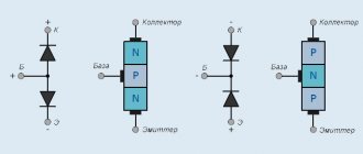
Symmetrical trigger assembled according to a standard circuit using bipolar transistors
In this publication, in addition to types of triggers, hardware and software are discussed. Examples of typical circuit solutions will be useful for creating workable structures with your own hands.
Story
A functional trigger can be created from a conventional relay with an electromechanical drive. By properly setting the control circuit contacts, the power group is turned on after a certain combination of input signals. A separate key performs a reset.
RS trigger circuit on one relay
Electronic analogues were assembled at the beginning of the last century from lamp devices. The current schemes were first published by Russian and English scientists in 1918-20. Later, semiconductor transistors began to be used. Nowadays, corresponding devices are created using microelectronic technologies.
Definitions
Voltage unit
Given the excessive diversity, the terminology used should be clarified. The following list contains correct answers to the question what is a trigger:
- a device for recording (storing) data that supports two equilibrium states;
- base memory cell;
- switching element with several stability positions;
- a logical component capable of transitioning to the “1” or “0” state with direct and reverse (inverse) output.
Classification
Capacitor energy
Products in this category are divided into two main groups based on the principle of control signals. In the first, a specified sequence of output signals is generated if the state is set to “1”. After moving to “0”, generation stops. The second is capable of switching the output voltage accordingly. Typically, "1" roughly corresponds to the power supply level.
Triggers are also distinguished according to the following parameters:
- synchronization of work cycles;
- static (dynamic) control methods;
- complexity of logic circuits;
- one- or two-stage.
Triggers on logic elements and on an operational amplifier
An amplifier circuit with two stages is well suited for implementing static triggers. The connection between them is organized directly or with limiting resistors in the corresponding circuits.
Trigger on logical elements
Schmitt Trigger
Products in this category can be created using different element bases. This section discusses the Schmitt trigger on transistors. It is controlled by changing an analog signal. Depending on the voltage level, the memory state is switched to the corresponding position “0” or “1”.
Schmidt trigger on transistors with a connected load
Symmetrical trigger. Principle of operation
Fig. 1 Symmetrical flip-flop circuit and diagram.
Figure 1 shows a circuit of a static symmetrical trigger using pnp transistors and a diagram of voltages on the collectors and bases. In each state of stable equilibrium, one of the transistors is open (in saturation mode), the other is closed (in cutoff mode).
Let transistor T1 be open and T2 be closed. In this case, the potential at the collector of transistor T1 is close to zero; and on the collector T2 is close to -Ek. A current is drawn from the base of transistor T1 through resistor R1″, keeping this transistor in a saturation state.
Transistor T2 is closed, since a positive bias voltage is formed at its base due to the source Ecm. Capacitor C1′ is practically discharged, and C1″ is charged to a voltage close to Ek. Due to the fact that the current gain of transistors in cutoff and saturation mode is zero, the total gain in the feedback loop is also zero. This ensures the stability of the described state.
The transition of a trigger from one stable state to another (i.e., its switching or overturning) is carried out by the action of an external trigger pulse on the bases or collectors of the transistors. (For more information about trigger triggering, see below.) Moreover, the parameters of the trigger signal must ensure that the transistors are brought into the active operating mode, when the current gain of the transistors is restored and positive feedback between the switches operates during the rollover time.
After tilting, a negative potential close to -Ek is established on the collector of transistor T1, and a potential close to zero is established on the collector T2. Capacitor C1′ is charged, and C1″ is discharged, and at the base of transistor T1, a positive potential is established, approximately equal to Ecm, and at the base of T2 a small negative potential is established (see diagram). The new stable state of the trigger is maintained until the next triggering pulse arrives.
Trigger what is it
The general principles of storage elements are presented above. A trigger is a device that can maintain 2 or more stable states that change under the influence of input signals. In fact, we are talking about a way to store the minimum amount of information - 1 bit.
What is measured in farads
Any trigger machine consists of two main blocks. The first one is intended for comparison or other type of processing of input signals. The second one provides data storage and status display with corresponding output signals:
- “1” – high level, straight, Q;
- “0” – low voltage, reverse (inverter), /Q.
As a rule, feedback is organized between functional blocks. Input signals are also divided into groups:
- informational – R, T, S;
- managers – V, C.
For your information. Operating cycles are described in tabular form, which clearly shows the state of the memory for different combinations of input signals.
Schmitt trigger operating principle
In an ideal case, the transfer characteristic of a Schmitt trigger has the form shown in the figure above. If the input voltage of the trigger does not exceed the response voltage U1 (UIN < U1), then the trigger is in one of the stable states, and the output voltage is at level E0 (UOUT = E0). When the input voltage exceeds the operating threshold (UBX > U1), the trigger will instantly switch to another stable state and the output voltage will become equal to the operating voltage of the trigger E1 (UOUT = E1). After this, the input voltage can change within certain limits, but the output will remain constant and equal to the operating voltage E1.
To return the Schmitt trigger to its original state, the input voltage must decrease to a certain level, called the trigger release threshold. As soon as the input voltage decreases to a certain voltage level U2 (UIN < U2), the trigger will jump to its original state, at which the output voltage will be equal to E0 (UOUT = E0).
The voltage values of the threshold levels of activation and release of the trigger are completely determined by the elements of the electronic circuit of this type of trigger.
As a rule, currently Schmitt triggers are manufactured in an integral design, the parameters of which are satisfactory in most cases. But in some cases, this type of triggers is also manufactured in discrete versions, for example, in experimental or high-voltage industries. Let's look at a discrete Schmitt trigger circuit using transistors.
Trigger Types
The following sections introduce the operating principles of standard devices. They can work independently or in various combinations. Combinations of flip-flops in electronics are used to build complex logic circuits.
What is trigger RS type
These elements are divided into groups according to control methods. For convenience, hereinafter the explanations are made using logical components. If necessary, you can assemble a similar trigger using relays or transistors.
RS trigger asynchronous
A workable circuit can be assembled from two standard NAND elements.
Circuitry, state table, signal graphs
RS trigger synchronous
In this scheme, when “1” is applied to C, the device provides “transparency” mode. Changes at the R and S inputs are reflected at intermediate points /R and /S with minimal internal delay. After setting the control signal to “0”, data storage is enabled.
Switching states occurs only in the presence of a control (clock) signal
D-triggers
Devices in this category are characterized by a time delay in the operating cycle.
D-flip-flop synchronous
The operation graphs show that a change in the output signal occurs only if there is a “1” at input C. The data is stored in an unchanged state until the next synchronization pulse arrives. This cycle ensures unhindered data flow.
These devices have a separate input for information signals
D-trigger two-stage
As in the previous example, one data channel is used here - D. The diagram shows how a more complex device is created from two single-stage blocks.
Two-stage latch with clock control
T-triggers
These devices perform the functions of elementary counters.
T-flip-flop asynchronous
Implementation of a counter using “AND-NOT” elements
T-flip-flop synchronous
Such devices are suitable for halving the frequency. The picture shows counters assembled on the basis of RS and D type triggers.
One output signal is generated for every two clock pulses
JK trigger
The operating cycles of this device are similar to the RS type trigger discussed above. The main difference is the change in the output signal to the opposite value (inversion) of the output signal after applying “1” to K and J simultaneously. It should be emphasized that there are no prohibited combinations in information channels.
Circuit assembled using “AND-NOT” elements
Universal trigger (JK trigger)
Such a trigger has information inputs J and K, which in their influence are similar to the inputs S and R of a clocked RS trigger:
- when J=1, K=0, the clock pulse trigger is set to state Q=1;
- when J= 0, K=1 – switches to state Q=0;
- when J=K=0 – stores previously received information.
But unlike a synchronous RS flip-flop, the simultaneous presence of logical 1s at the information inputs is not a prohibited combination for a JK flip-flop and leads the flip-flop to the opposite state.
JK flip-flop transition table
| K | J | C | Q(t) | Q(t+1) |
| 1 | ||||
| 1 | 1 | 1 | ||
| 1 | 1 | 1 | ||
| 1 | 1 | 1 | 1 | |
| 1 | 1 | |||
| 1 | 1 | 1 | ||
| 1 | 1 | 1 | 1 | |
| 1 | 1 | 1 | 1 |
Digital electronics – YB-triggers with dominant Y-input
The presence of forbidden combinations for clocked &Y flip-flops gave rise to the idea of building a trigger that forcibly sets Qx to 0 at S = 1 and R = 1 when a clock pulse is applied. This becomes possible thanks to a special connection of the inputs. In Fig. Figure 7.35 shows such a connection of inputs. When S = 1 and R = 1, the 1-signal cannot affect the flip-flop, since the output of the element is NOT 0. The AND-element is locked. 1-signal on R allows reset. The setting mode with S = 1 and R = 0 remains possible, since now the output of the NOT element is 1 and the AND element has a 1 at the output.
Interesting article: What is a solid state relay?
Such a trigger is called an .RS'-trigger with a dominant /?-input, or a ^trigger. The rule of its operation follows from the symbol in Fig. 7.36 (see also section 7.1). It says: if both inputs of the trigger S, R and input T have level 1, then with a synchronization signal 1 Q{ is set to 0, and Q2 is set to 1. The truth table of a clocked LU flip-flop with a dominant R-input is shown in Fig. 7.37. Of course, there is also a clocked RS flip-flop with a dominant ^-input (see reference test).
It will be interesting➡ What is a short circuit
Synchronous and asynchronous triggers
These groups are created on the principle of dependence of output states on clock pulses.
Asynchronous triggers
Products of this type change the state of stored information after receiving the corresponding input data. The slight delay is explained by the time it takes for the signal to travel through the chain of switching elements of the circuit.
Synchronous triggers with dynamic clocking
This group contains products controlled by synchronizing pulses. State switching is performed on a rising or falling edge. When there is no activity in C, the data is stored in an unchanged state, regardless of the arrival of new information.
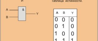
1) Combination logic, basic elements (and, or, not), their circuits on CMOS transistors.
Combination circuit
– a logical circuit whose output signal is determined only by the signal levels at its inputs. This approach to constructing circuits is called combinational logic.
Logic elements
– devices designed to process information in digital form (sequences of signals of high “1” and low “0” levels).
Basic logic elements
| 1) Valve I (AND) | If at least one input is “0”, then the output is “0” |
| 2) OR valve | If at least one valve is “1”, then the output is “1” |
| 3) NOT valve – inverter | Nowadays almost everything is built using inverters. If we take NAND or NOR, then by connecting the inputs we get an inverter |
Circuits based on CMOS transistors
Repetition on the topic FIELD TRANSISTORS
0 – blocks n-channel transistor 1 – opens the n-channel transistor (with p-channel it’s the other way around) | n-channel – arrow to gate p-channel – shutter arrow |
The LE on the DC are based on inverters (switches). Let's consider the logical elements AND-NOT and NOR-NOT, as well as an inverter.
1) NAND
(and + inverter) on CMOS transistors
( NAND )
| Example: At input A and B “1”: Tr1 – closed; Tr2 – closed; Tn1 – open; Tn2 – open, so the output is “0” Truth table: |
2) NOR
(or + inverter) on CMOS transistors
( NOR )
| Example: At input A and B “1”: Tr1 – closed; Tr2 – closed; Tn1 – open; Tn2 – open, so the output is “0” Truth table: |
3) NOT gate on CMOS transistors
| 1. At input “1”, VT1 is closed; VT2 is open, so the output is “0” 2. At the input “0”, VT1 is open; VT2 is closed, so the output is “1” |
Explanation of how the inverter works (pictures C and D):
2) RS trigger. The simplest trigger on bipolar transistors. RS flip-flop based on logical elements AND-NOT, OR-NOT. Synchronous RS trigger.
Trigger
– a device that has the ability to remain in one of 2 stable states for a long time and alternate them under the influence of external signals.
The property of “memorizing” binary information is the ability to remain in one of two states (remembers “1” or “0”)
When power is turned on, the trigger unpredictably assumes one of two states.
Bipolar transistor trigger
The device circuit consists of cascades made of transistors. The input of each of them is connected to the output of the opposite one.
Let VT2 be closed at the initial moment of time. Under the influence of voltage on its collector, a current flows through Rb3, holding VT1 in the open state. At the same time, open VT1 short-circuits the base circuit of transistor VT2 with resistor Rb4. The closed state of VT2 corresponds to the output value Q=1. Open state VT1 =0. The voltage at the collector of a closed transistor (Q=1) is equal to: UQ=Up×Rb3/(RK2+Rb3) | In order to change the trigger state to the opposite one, it is necessary to apply signals to the R or S input. Input signals are usually pulsed. The presence of voltage at the S input (S=1) sets Q=1, and the presence of voltage at the R input (R=1) sets Q=0. Simultaneous supply of a signal to inputs S and R is prohibited, because the trigger in this case ceases to be a trigger (there will be no opposite state Q and ). |
| Diagrams of operation in the presence of input pulse signals. During the interval between pulses at the S and R inputs, the trigger remembers the state to which it was set by these inputs, i.e. trigger is a memory element. |
Trigger on logical elements
The RS trigger is named after its inputs.
Input S (Set – installation) allows you to set the output of trigger Q to a single state (write one). Input R (Reset) allows you to reset the output of the trigger Q to the zero state (write zero).
The trigger has two outputs Q – direct and – inverse. The state of the trigger is determined by the state of the direct output.
The RS flip-flop is assembled on the basis of two logical elements: OR-NOT and NAND. The difference is that the trigger on the
AND-NOT is transferred to another state by the potential of logical zero ( active level - low ). A trigger assembled on OR-NOT is activated by a logical unit ( active level - high ).
To describe the operation of the trigger, a table of states (transitions, truth) is used.
Let us describe the operating principle of an RS flip-flop assembled using NOR elements.
If we apply an active level to R, then the output will be “0”
If we apply an active level to S, then the output will be “1”
State 0-0 – storage of the previous state State 1-1 – uncertainty | Q(t) – state of the trigger before the arrival of control signals (changes at inputs R and S); Q(t+1) – trigger state after changes at inputs R and S. |
Let R=0, S=1. The lower logical element performs the logical OR-NOT function, i.e. “1” at any of its inputs leads to the fact that its output will be logical zero = 0. The output Q will be “1”, because zeros are supplied to both inputs of the upper element (one zero from input R, the other from output). The trigger is in the single state
.
If we now remove the setting signal (R=0, S=0), the situation at the output will not change, because Although the lower input of the lower logic gate will receive a 0, its upper input will receive a 1 from the output of the upper logic gate. The trigger will be in the single state until a reset signal is received at the R input
.
Let now R=1, S=0. Then Q=0, a =1. The trigger switched to "0".
If after this you remove the reset signal (R=0, S=0), then the trigger will still not change its state.
Let us describe the operating principle of an RS flip-flop assembled using NAND elements.
Inputs R and S are inverse (active level “0”). The transition (switching) of this trigger from one state to another occurs when one of the inputs is set to “0”. The combination R=S=0 is prohibited.
Synchronous
RS flip-flop
Since control signals can come as they please, a synchronous RS flip-flop was proposed (a synchronization circuit was added), i.e. switching will only occur if there is a synchronized signal.
3) Static D trigger, circuit, operating principle. Truth table of D flip-flop. Schematic diagram of a static D flip-flop using AND-NOT, NOR-NOT elements. Dynamic D triggers. Timing diagrams of the D flip-flop.
A D-flip-flop is a flip-flop with one information input that operates in such a way that the output signal after switching is equal to the signal at input D before switching, i.e. Qn+1=Dn The main purpose of D-flip-flops is to delay the signal applied to input D. It has an information input D (data input) and a synchronization input C. The synchronization input C can be static (potential) and dynamic. For flip-flops with a static input C, information is recorded during the time at which the signal level C = 1. In flip-flops with dynamic input C, information is recorded only during the voltage drop at input C. The dynamic input is depicted in diagrams as a triangle. If the vertex of the triangle is facing towards the microcircuit (direct dynamic input), then the trigger is triggered by the edge of the input pulse, if away from it (inverse dynamic input) - by the edge of the pulse. In such a flip-flop, the output information can be delayed by one clock cycle relative to the input information.
If the signal level at input C = 0, the trigger state is stable and does not depend on the signal level at information input D. When a level C = 1 is applied to the synchronization input, the information at the direct output will repeat the information supplied to input D. Therefore, when C = 0 Qn+1=Qn, and for C=l Qn+1=Dn.
My comments:
- The line / or \ at the C-input of the trigger means that the dynamic trigger operates either on the edge of the input pulse (beginning) or on the edge (end). More often, similar images of a triangle are used, turned towards the trigger or away from it.
- Figure 1 shows the circuit of a D-trigger in the AND basis, we do not need it, the necessary circuits are indicated in Figures 2 and 3.
- Transparent latch is the same as a static flip-flop. A delay flip-flop is an alternative name to a dynamic flip-flop.
- Excerpt from the synopsis: can store 1 bit of information, a register can be assembled from several D-triggers.
Figure 1 – Timing diagrams of the D-flip-flop, truth table, symbol of a dynamic D-flip-flop (it differs from a static one by the “/” line at the C-input)
Figure 2 – D-flip-flop circuit in the NAND basis
Figure 3 – D-flip-flop circuit in the NOR basis
4) T-trigger (counting trigger). T flip-flop circuit (based on D flip-flop). 4-bit summing counter based on T-flip-flops, its timing diagram. 4-bit subtractive counter based on T-flip-flops, its timing diagram.
Abstract: A D flip-flop with a dynamic C input can work as a T flip-flop. To do this, you need to connect input C to the inverse output of the trigger /Q. A counter can be assembled from a T-flip-flop. Knowing the pulse duration, you can adjust the time intervals (LED blinking)
Figure 4 – Conversion of a D-trigger into a T-trigger and its timing diagram
From a dynamic D-flip-flop, you can assemble a T-flip-flop: the trigger input is clock (C), and the data input (D) is combined with an inverted output. Such a flip-flop has only one input
. When the input clock pulse is applied, the output switches on the falling edge.
Figure 5 – Schematic representation of a T-flip-flop
Working principle of T-flip-flop
After a pulse arrives at input T, the state of the trigger changes to the exact opposite. It is called counting because the T-flip-flop counts the number of pulses received at its input.
The only pity is that this trigger can only count up to one. When the second pulse arrives, the T-trigger is reset to its original state again.
| Q switches on the falling edge of C. This is a kind of “frequency (signal) divider” |
Figure 6 – What is a front (just in case)
A counter is a device, a set of signals at the output of which in a certain code displays the number of pulses received at its input.
By combining T-flip-flops we get counters (either adding or subtracting). Triggers are connected in series, so that the output of the previous one is connected to the input of the next one.
Number of counted pulses NMAX = 2m, m – number of triggers.
4-bit sum counter based on T-flip-flops, its timing diagram
The counter circuit, which allows you to count any number of pulses less than sixteen, is shown in the figure below. The number of pulses received at the input can be found by connecting to the counter outputs Q0 ... Q3. This number will be represented in binary code.
Figure 7 – 4-bit summing counter based on T-flip-flops
Let the initial state of all counter triggers be zero. We see this state in timing diagrams. Let's write it in Table 1. After a clock pulse (which is perceived at the falling edge) arrives at the input of the counter, the first trigger changes its state to the opposite, that is, one. Let's write the new state of the counter outputs into the same table.
Since upon arrival of the first pulse the state of the first trigger changed, this trigger contains the least significant bit of a binary number (one). In the table we will place its value at the very right place, as is customary when writing any multi-digit numbers.
Let's apply another clock pulse to the counter input. The value of the first trigger will again change to the exact opposite. This time, a falling edge will form at the output of the first trigger, and therefore at the input of the second trigger. This means that the second trigger will also change its state to the opposite.
Continuing to analyze the timing diagram, we can determine that numbers from 0 to 15 appear sequentially at the outputs of the above counter circuit. These numbers are written in binary form. When the next pulse arrives at the counting input of the counter, the contents of its triggers increase by 1. Therefore, such counters are called summing binary counters.
Table 1 – Change in levels at the output of the summing counter when pulses arrive at its input.
4-bit subtractive counter based on T flip-flops, its timing diagram
Counters can not only increase their value by one when pulses arrive at the counting input, but also decrease it. Such counters are called subtractive counters. To implement a subtractive counter, it is enough for the T-flip-flop to change its state at the leading edge of the input signal.
You can change the working edge of the input signal by inverting this signal.
Figure 8 – 4-bit subtractive counter based on T flip-flops
The diagram shows that when the first pulse arrives at the input of the counter, the maximum number possible for a four-bit counter appears at the outputs. When the next pulses arrive, the counter contents are decreased by one.
This is because when the rising edge of the clock pulse arrives, the first flip-flop goes into the one state. As a result, a leading edge is also formed at its output. It enters the input of the second trigger, which leads to the recording of one in this trigger as well. Exactly the same situation occurs with all triggers of the counter, that is, all triggers will go into the single state.
The next clock pulse will lead to a change in the state of only the first trigger, since at the same time a falling edge of the signal will be formed at its output. Please note that with the arrival of each subsequent pulse, the contents of the counter built according to the analyzed circuit are reduced by one.
Table 2 – Change in levels at the output of the subtractive counter when pulses arrive at its input.
5) Registers based on D-flip-flops. Parallel registers, serial (shift) registers. Timing diagram of the shift register operation.
The shift register is built on four D flip-flops with dynamic input blocking. To manage the register, the following are formed:
- input C - synchronization input
- input R - general register reset.
Registers based on D flip-flops
Based on dynamic D-flip-flops, we can assemble registers.
A single D-trigger is the simplest memory cell that can store 1 bit of information. Therefore, it makes sense to combine dynamic D-flip-flops into assemblies of 4, 8 (there will be so many bits, a 4-bit register, etc.).
Figure1 – left-parallel, right-sequential
Parallel registers
- All D-flip-flops are combined in parallel
- We provide information at all inputs
- Clock pulse writes new information
- Inf appears on the outputs
- Until a new clock pulse appears, a new portion of data will be saved
Sequential (shift) registers.
Data is supplied only to the 1st dynamic D-trigger
A serial input shift register is a device in which data is input serially.
Used to convert serial data into parallel format.
Figure2 – Typical 4-bit register with serial input
In this case, D-triggers are used. The register works as follows.
- In the initial position, a reset pulse (logical 0) is applied to the “Set to 0” input, setting outputs Q0-Q3 to 0.
- Next, the first bit of data is applied to the serial input.
- When exposed to the rising edge of the first clock pulse, Q0 takes on a value equal to D1.
- D2 is then applied to the serial input.
- When exposed to the rising edge of the second clock pulse, Q0=D2 and Q1=D1.
- After four clock pulses we have Q0=D4, Q1=D3, Q2=D3, Q3=D1.
The data output can be either serial or parallel. In the latter case, the shift register operates as a serial-to-parallel converter. Obviously, for shift registers that have a large number of bits (more than eight), parallel outputs are not practical due to the large number of outputs in the IC package. There are shift registers with more than 1000 bits.
Physical implementations of triggers
The base element is created from semiconductor devices using modern technological processes to miniaturize functional products.
Logic element based on MOS transistors
Triggers with thyristors
To increase the power of the connected load, you can assemble a trigger using thyristors. Input S is connected to the control electrode, and input R is connected to the gate. To maintain a constant voltage at the anode, a transistor connected to the appropriate circuit is suitable.
Triggers on relay-contactor base
Despite the general trends of miniaturization, it is quite possible to create a functional trigger from a relay. Such solutions, in particular, are used to protect power circuits when turning on powerful electric drives.
Advantages of using flip-flop logic circuits
Having figured out what a trigger means, it’s easy to use the knowledge gained to solve practical problems. Using logical elements:
- automate the operation of lighting systems;
- provide safe connection of machines and other powerful loads;
- prevent dangerous conditions using signals from external sensors.
To create a high-quality device based on triggers, it is recommended to use the presented information in combination. The actual operating conditions must be taken into account in order to select suitable functional components of the design.