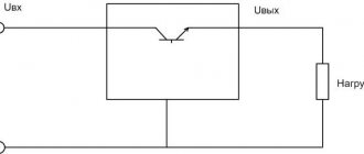
For the correct functionality of many electrical devices, it is necessary to maintain certain operating parameters of the power supply network. If the voltage goes beyond the normal range, it is accompanied by a deterioration in efficiency. Pulse interference causes malfunctions. A current stabilizer on a field-effect transistor, the circuit of which is presented in this publication, will help correct the situation.
Powerful field-effect transistor power supply
Operating principle (current stabilizer operation)
Let our load be R, we will assume that its resistance almost does not change (R = const), we want the current unchanged (I = const), and what remains for us is only the output voltage at the current source, this is what the circuit will select , and not just from the bulldozer, but precisely one in which exactly the current I for which the device is designed will flow through the above-mentioned load R.
And here is an analysis of the operation of the circuit itself:
after connecting the power source, the field-effect transistor opens through resistor R1, current flows through resistor R2—the open drain-source channel VT1—and the load (LED). The higher the current, the more the voltage across the resistor will drop, and when it reaches the opening value of VT2 (for silicon bipolar approximately 0.60-0.75 V), it will open, current will flow through its EC from the minus to the gate of VT1, thereby closing it, but not completely, because R1 is not going anywhere.
Note. Parts for this instance were taken from old boards, in particular, a powerful field-effect N-channel transistor MTD20N06V in DPAK (TO-252) version from the motherboard, it has an open channel resistance of 65 mOhm, and a maximum long-term applied gate-source voltage of 20 Volts, which powers the circuit from the power supply 12 Volts (voltage surges no more than a few Volts), so a Zener diode is not needed. The bipolar transistor is the well-known BC847A in a SOT-23 package. Resistor R1 = 11 kOhm , R2 = 2 Ohm , size 1205 and power 0.25 W. This instance is designed for stabilized current:
Istab = UBE * R2 = 0.6 V / 2 Ohm = 300 mA
Current stabilization principle
The purpose of the special circuit is to regulate the power source in automatic mode to maintain stable parameters of the load circuits. The main component is a fairly powerful semiconductor device, a current limiter at the output of the power supply.
Requirements for the control element
Selection criteria can be formulated if the current parameters (amperes) are known. However, even without a specific technical specification, it is easy to list the basic requirements:
- the current in the control circuit is maintained with a certain accuracy;
- differences in power consumption should be compensated;
- corrective changes must be made quickly enough;
- To automatically adjust the optimal mode and improve protection against interference, feedback is needed.
The essence of stabilization
To clarify the functionality of the control element, it is necessary to note the features of a typical load. The emission intensity of an LED, for example, significantly depends on the temperature during operation. The power consumption changes accordingly. As the current increases, the voltage decreases.
Important! If feedback (negative) is established, the noted change will regulate the operating mode of the control device. In particular, as the voltage between the gate and drain of the FET increases, the current through the source decreases. Thus, stabilization of the source’s output parameters is ensured without any other additional actions.
Trial
The tracks were drawn with a marker, so the board is slightly different from the designed one; fastenings for the screws were not made.
We connect the device to a power source (I had a 12V transformer with a diode bridge and a capacitor), now knowing that the current is relatively small, I stupidly shorted the output with an ammeter designed to measure direct current up to 20A, the readings are below: This is an adequate result for such a circuit. Next, two 10 W LEDs with different supply voltages were connected in turn. For an LED with one crystal, the voltage output was Uout = 2.72 V at a current Iout = 0.31 A, while at the input Upit = 10.88 V, i.e. dissipates approximately:
P1 = (Upit - Uout)*Iout = (10.88-2.72)*0.31 = 8.16*0.31 = 2.53 W
For the second LED, in which three crystals are connected in series Uout = 10.32 V, Iout = 0.29 A at Upit = 11.22 V, we obtain:
P2 = (Upit - Uout)*Iout = (11.22-10.32)*0.31 = 0.9*0.31 = 0.279 W
When the input voltage differs as little as possible from the required supply voltage to provide the required current, then high efficiency is achieved (with a second LED η = 92%) with ease of implementation.
Let's replace the resistor that determines the output current of the current source with 470 Ohms, then we get the output current:
Iout = UBE/R2 = 0.6 / 471 = 1276 µA
Ammeter test:
Thus, with a 12 V power supply, we connect a 5 mm LED, a current of ~1.3 mA passes through it, through two/three LEDs the current will be the same, because the supply voltage is enough for this.
I also made a small graph of the dependence of the output stable current on the supply voltage of the current stabilizer. First, the rated current is reached (when the supply voltage is not enough for Ist), and then everything is fine, when the voltage changes three times (from 10 to 30 V), the current changes by only 0.64 mA or 4.22%.
Selecting a connection scheme
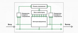
In practice, different engineering solutions are used. In particular, manufacturers offer switching power supplies to connect LED lamps. These devices perform their functions using frequency conversion and signal modulation. Microchips are installed to control the key. A throttle is used for measured energy storage.
Pulse current stabilizer
For simplicity, this article considers linear stabilization. Devices created according to this scheme do not create strong electromagnetic interference. This is the main difference from pulse analogues.
Increased stability
During operation, part of the energy is dissipated, the board and circuit components heat up, the parameters fluctuate, and most importantly, the saturation voltage (UBE) of transistor VT2 changes, the same ~0.7 V will change, which will lead to a change in the output current.
TKN ( Temperature Voltage Coefficient pn junction of the transistor is negative; with increasing temperature, UBE will decrease . For thermal stabilization, we introduce an additional element with a positive TKN - a zener diode (with Ust > 6.5 V), then when heated, the voltage on one component (VT2) will decrease, and on the other (D1) will increase, thus compensation is obtained. Ideally, the TKN of both devices should be equal in magnitude and opposite in sign, and heating should occur equally (that is why they are located next to each other on the board).
Another transistor VT3 has also been added, which acts as a current source for VT2, which will give even greater stability, because when the supply voltage changes within a certain range, the base current of VT2 will hardly change.
Design and operation of a field-effect transistor
DIY 220V voltage stabilizer circuit
To study the functionality of a field-effect transistor, you can consider two connection diagrams. In the first option, the source and gate are connected with a conductor, leveling the corresponding potential: Uzi = 0. By increasing the voltage Usi (drain-source), current flows in the working area.
Voltage is zero
In the state shown in the figure, the device functions as a typical conductor. The specific name on the graph “Ohmic region” defines the zone of proportional increase in current strength as the potential difference increases. When entering the saturation mode, the number of free charges is not enough to maintain the noted change.
Reducing gate potential
In this figure, the charge passage channel is narrowed by an additional power source, which reduces Uzi<0. At a certain level (cut-off voltage) no current flows.
Field effect transistor device
The figure shows p and n type zones. By adjusting the voltage Usi, the channel resistance (current strength) is changed. As shown above, this circuit can be closed if necessary.
Printed circuit boards
Silkscreen only: pcb_current_source_silk.pdf Tracks only: pcb_current_source_solder.pdf Tracks and silkscreen: pcb_current_source_solder_silk.pdf Silkscreen only: pcb_current_source_silk.pdf Tracks only: pcb_current_source_improved_solder.pdf Tracks and silkscreen: pcb_current_source_improved_solder_silk.pdf
Everything fits on a small piece (3 by 2 cm) of foil PCB, heat is removed by attaching the entire board to a piece of aluminum with screws, it is designed with M2 fasteners in mind to easily and reliably fix it or simply glue it to the heat sink with heat-conducting glue (Stars 922) . If necessary, it can be easily reduced by almost half.
A simple two-polar voltage regulator on LM317.
The device is based on the circuit described above, and a negative voltage stabilization arm is added.
Characteristics and advantages of a two-polar stabilizer
- stabilization voltage from 1.2 to 30 V;
- maximum current up to 5 A;
- a small number of elements are used;
- simplicity in choosing a transformer, since you can use the secondary winding without a central tap;
The parts are installed on one-sided fiberglass. Transistor VT1, VT2 and microcircuits LM317 and LM337 should be installed on radiators. When installing on a common radiator, insulating gaskets and bushings should be used.
List of components
| Designation | Description | Buy on Aliexpress |
| VT1 | Powerful field effect transistor | 10pcs 2SK3919 TO-252 K3919 TO252Price: 0.98$ + 0.32$ = 1.3$ |
| VT2 | Low power transistor | 100pcs/lot BC847B SOT-23 BC847 SOT SMD 847B SOT-23Price: 0.79$ |
| R1, R2 | Resistors 1205 0.25 W (pack of 660 pcs.) | 1206 SMD Resistor Kit Assorted Kit 1ohm-1M ohm 1% 33valuesX 20pcs=660pcsPrice: 3.20$ |
| Thermally conductive adhesive Stars 922 | Star-922 Thermal Paste Thermal Grease Silicone Price: 1.54$ |
12V linear voltage regulator circuit
Linear stabilizers use KREN chips, as well as LM7805, LM1117 and LM350. It should be noted that the KREN symbol is not an abbreviation. This is an abbreviation of the full name of the stabilizer chip, designated as KR142EN5A. Other microcircuits of this type are designated in the same way. After the abbreviation, the name looks different - KREN142.
Linear stabilizers or DC voltage regulators are the most common. Their only drawback is the inability to operate at a voltage lower than the declared output voltage.
For example, if you need to get a voltage of 5 volts at the output of the LM7805, then the input voltage must be at least 6.5 volts. When less than 6.5V is applied to the input, a so-called voltage drop will occur, and the output will no longer have the declared 5 volts. In addition, linear stabilizers get very hot under load. This property underlies the principle of their operation. That is, voltage higher than stabilized is converted into heat. For example, when a voltage of 12V is applied to the input of the LM7805 microcircuit, then 7 of them will be used to heat the case, and only the necessary 5V will go to the consumer. During the transformation process, such strong heating occurs that this microcircuit will simply burn out in the absence of a cooling radiator.
In the end
Such a conditional current source can be used as a current stabilizer for LEDs in a car (12 V-14.4 V), using it to connect lasers to some kind of transformer or UPS with a jumping voltage of several volts, or use it in charger circuits. But, as you understand, this device can be used with any other load that requires a stable electric current. This stabilizer dissipates “extra” energy in the form of heat, which may be unacceptable in situations where the voltage difference is large and the flowing current is not small, but, for example, in conditions where the input voltage does not greatly exceed the output voltage and the stabilization current is small, why not? ?
An example of a field-effect transistor stabilizer
When creating radio devices using lamps, a typical anode power supply does not provide the necessary stability of output parameters. Adding a resistor to the circuit increases losses and does not allow accurate adjustment of power changes in the load.
Electrical circuit of a simple stabilizer
It is not difficult to assemble this current stabilizer on a field-effect transistor with your own hands. With its help, the accuracy of the specified parameters is ensured in a range of no more than 6% of the nominal value.
Stabilized regulated power supply with overload protection
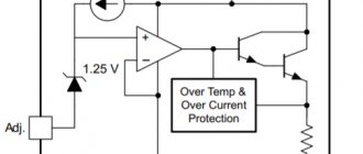
Many amateur radio power supplies (PS) are made on KR142EN12, KR142EN22A, KR142EN24, etc. microcircuits. The lower limit of adjustment of these microcircuits is 1.2...1.3 V, but sometimes a voltage of 0.5...1 V is necessary. The author offers several technical power supply solutions based on these microcircuits.
The integrated circuit (IC) KR142EN12A (Fig. 1) is an adjustable voltage stabilizer of the compensation type in the KT-28-2 package, which allows you to power devices with a current of up to 1.5 A in the voltage range 1.2...37 V. This integrated stabilizer has thermally stable current protection and output short circuit protection.
Fig.1. IC KR142EN12A
Based on the KR142EN12A IC, you can build an adjustable power supply, the circuit of which (without a transformer and diode bridge) is shown in Fig. 2. The rectified input voltage is supplied from the diode bridge to capacitor C1. Transistor VT2 and chip DA1 should be located on the radiator. Heat sink flange DA1 is electrically connected to pin 2, so if DA1 and transistor VD2 are located on the same radiator, then they need to be isolated from each other. In the author's version, DA1 is installed on a separate small radiator, which is not galvanically connected to the radiator and transistor VT2.
Fig.2. Adjustable power supply on IC KR142EN12A
2.06. Transistor current source
CHAPTER 2. TRANSISTORS
SOME BASIC TRANSISTOR CIRCUITS
Subsections: 2.02 2.03 2.04 2.05 2.06 2.07 2.08 2.09
Although current sources are not as well known, they are no less useful and important than voltage sources. Current sources are an excellent means of biasing transistors, and are also indispensable as resistive loads for high-gain amplifier stages and as emitter supplies for differential amplifiers. Current sources are necessary for the operation of devices such as integrators and sawtooth voltage generators. In amplifier and stabilizer circuits, they provide a wide range of voltages. And finally, direct current sources are required in some areas that are not directly related to electronics, for example, in electrochemistry and electrophoresis.
Rice. 2.20.
Connecting a resistor to a voltage source. The circuit of the simplest current source is shown in Fig. 2.20. Provided that Rн » R (in other words, Un » U), the current remains almost constant and is approximately equal to I = U/R. If the load is a capacitor, then, provided that Ucond » U, it charges at an almost constant rate determined by the initial portion of the exponential characteristic of a given RC circuit.
The simplest resistive current source has significant disadvantages. In order to get a good approximation to the current source, higher voltages must be used, and in doing so, more power is dissipated in the resistor. In addition, the current of this source is difficult to control over a wide range using a voltage generated elsewhere in the circuit.
Exercise 2.6.
Let's say we need a current source that would provide an accuracy of 1% in the load voltage range from 0 to +10 V. Which voltage source should be connected in series to the resistor?
Exercise 2.7.
Let's say that in the previous exercise you need to receive a current of 10 mA from a source. How much power will be dissipated by the resistor? How much power is transferred to the load?
Rice. 2.21. Transistor current source: basic idea.
How much power is transferred to the load? Transistor current source. A very good current source can be built based on a transistor (Fig. 2.21). It works as follows: a base voltage Ub > 0.6 V maintains the emitter junction in the open state: Ue = Ub - 0.6 V. In this regard, Ie = Ue / Re = (Ue - 0.6 / Re. So as for large values of the coefficient h21eIe ≈ Ik, then Ik ≅ (Ub - 0.6 V)/Re regardless of the voltage Uk until the transistor goes into saturation mode (Uk > Ue + 0.2 V).
Mixing in the current source. The base voltage can be generated in several ways. A good result is achieved by using a voltage divider if it provides a fairly stable voltage. As in previous cases, the resistance of the divider should be significantly less than the resistance of the circuit on the base side for direct current h21еRe. You can also use a Zener diode and use the Ucc power supply for biasing, or you can take several diodes, forward biased and connected in series, and connect them between the base and the corresponding emitter power supply. In Fig. Figure 2.22 shows examples of bias circuits. In the last example (Fig. 2.22.6), a pnp-type transistor supplies current to a grounded load (it is a current source). The remaining examples (in which n-p-n transistors are used) would be more correctly called “sinks” of current, but it is customary to call all circuits of this type current sources. [The names "sink" and "source" are related to the direction of the current; if current flows to any point in the circuit, then this is the source, and vice versa]. In the first circuit, the resistance of the voltage divider is approximately 1.3 kOhm and is very small compared to the resistance on the base side, which is ≅100 kOhm (for h21e = 100). Any change in β due to a change in collector voltage will not significantly affect the output current, since the corresponding change in base voltage is very small. In the other two designs, the resistors in the bias circuit are chosen so that the current flowing is a few milliamps, enough to keep the diodes open.
Working range. The current source supplies direct current to the load only up to a certain final voltage across the load. Otherwise, the current source would be capable of generating infinite power. The range of output voltage over which the current source behaves as expected is called the operating range. For the transistor current sources just discussed, the operating range is determined from the fact that the transistor must be in the active operating mode. So, in the first circuit, the voltage on the collector can be lowered until saturation mode is reached, i.e., up to +12 V. The second circuit, with a higher voltage on the emitter, retains the properties of the source only up to the value of the voltage on the collector, equal to approximately + 5.2 V.
In all cases, the collector voltage can vary from the saturation voltage to the supply voltage. For example, the latter circuit operates as a current source over a load voltage range limited to 0 and +8.6 V. If the load uses batteries or its own power supplies, the collector voltage may be greater than the power supply voltage. When using such a scheme, it is recommended to keep an eye on it. so that a breakdown of the transistor does not occur (the voltage Uke should not exceed the value Ukeprob - the breakdown voltage of the collector-emitter junction) and excess power is not dissipated (determined by the value of the product IkUke). In Sect. 6.07 you will see that for high-power transistors the safe operating area is specifically defined.
Exercise 2.8.
The circuit has two stabilized voltage sources: +5 and 15 V. Design a current source circuit based on an npn transistor - a type that would provide a current of +5 mA. Use a +5 V source as the voltage source for the base. What is the operating range in such a circuit?
In a current source, the base voltage does not have to be fixed. If we provide for the possibility of changing the voltage Ub, we obtain a programmable current source. If the output current should smoothly track changes in the input voltage, then the swing of the input signal uin (we remind you that we agreed to denote changes with lowercase letters) should be small, such that the voltage at the emitter never decreases to zero. In such a current source, the change in output current will be proportional to changes in the input voltage.
Disadvantages of current sources. How much does a transistor current source differ from an ideal one? In other words, does the current in the load change when, say, voltage changes, i.e. does the current source have an equivalent resistance of finite value (Req
1. For a given collector current, both the voltage Ube and the coefficient h21e (Early effect) change slightly as the collector-emitter voltage changes. A change in voltage Ube associated with a change in voltage across the load causes a change in the output current, since the voltage at the emitter (and therefore the emitter current) changes, even if the base voltage is fixed. Changing the value of the coefficient h21e leads to small changes in the output (collector) current at a fixed emitter current, since Ik = Ie - Ib; in addition, the voltage at the base changes slightly due to a possible change in the resistance of the mixing source due to changes in the coefficient h21e (and, consequently, the base current). These changes are minor. For example, a change in the output current for the circuit shown in Fig. 2.22, a, is approximately 0.5% for a 2N3565 type transistor. In particular, when the load voltage changes from 0 to 8 V, the Early effect causes a change in current by 0.5%, and heating of the transistor by 0.2%. Changing the coefficient makes an additional contribution to the change in output current - 0.05% (for a rigid voltage divider). All these changes result in a current source that performs worse than ideal: the output current varies slightly with voltage and therefore its resistance is not infinite. In the future, you will learn that there are methods that can overcome this disadvantage.
2. Voltage Ube and coefficient h21e depend on temperature. In this regard, when the ambient temperature changes, a drift of the output current occurs. In addition, the junction temperature changes as the load voltage changes (due to changes in the power dissipated by the transistor) and causes the source to perform less than ideally. The change in voltage and Ube depending on the ambient temperature can be compensated using the circuit shown in Fig. 2.23. In this circuit, the voltage drop between the base and emitter of transistor T2 is compensated by the voltage drop across the emitter junction T1, which has the same temperature characteristics. Resistor R3 plays the role of a load for T1, necessary to set the inflowing current of the base of transistor T2.
Rice. 2.23. One of the methods of temperature compensation of a current source.
Improving the characteristics of the current source. Generally speaking, the change in voltage Ube caused by both the influence of temperature (the relative change is approximately -2 mV/°C) and the dependence on voltage Ube (the Earley effect is estimated at ΔUbe ≈ -0.001 ΔUke) can be minimized by setting the voltage on the emitter is large enough (at least 1 V), then a change in voltage Ube by tenths of a millivolt will not lead to a significant change in the voltage across the emitter resistor (remember that the circuit maintains a constant voltage at the base). For example, if Ue = 0.1 V (i.e., a voltage of 0.7 V is applied to the base), then a change in voltage Ue by 10 mV causes a change in the output current by 10%, if Ue = 1.0 V, then the same a change in Ube causes a change in current by 1%. However, don't go too far. Let us recall that the lower limit of the operating range is determined by the voltage at the emitter. If in a current source operating from a +10 V power supply, the emitter voltage is set to +5 V, then the output range will be slightly less than 5 V (the collector voltage can vary from Ue + 0.2 V to Ucc, i.e. . from 5.2 to 10 V).
Rice. 2.24. Cascode current source with increased resistance to load voltage changes.
In Fig. Figure 2.24 shows a circuit that significantly improves the characteristics of the current source. The current source T1 operates as before, but the collector voltage is fixed by the emitter T2. The current flowing into the load is the same as before, since the collector (for T2) and emitter currents are approximately equal to each other (due to the large value of h21e). In this circuit, the voltage Uke (giving T1) does not depend on the voltage at the load, which means that changes in the voltage Ube caused by the Early effect and temperature are eliminated. For 2N3565 type transistors, this circuit gives a current change of 0.1% when the load voltage changes from 0 to 8 V; In order for the circuit to provide the specified accuracy, stable resistors with a tolerance of 1% should be used. (By the way, this circuit is used in high-frequency amplifiers, where it is known as a “cascode”). In the future, you will become familiar with current source circuits that use operational amplifiers and feedback, and in which the problem of eliminating the influence of changes in Ube on the output current is also solved.
The influence of the h21e coefficient can be weakened if you select a transistor with a large h21e value, then the base current will make a small contribution to the emitter current.
Rice. 2.25. Transistor current source using voltage Ube as a reference.
Figure 2.25 shows another current source in which the output current is independent of the supply voltage. In this circuit, the voltage Ube of transistor T1, falling across resistor R1, determines the output current regardless of the voltage Ucc
Uout = Ube/R2U2.
Using resistor R1, the bias of transistor T2 and the collector potential of T1 are set, and this potential is less than the voltage Ucc by twice the voltage drop across the junction; thereby reducing the influence of the Early effect. There is no temperature compensation in this circuit; the voltage across R2 decreases by approximately 2.1 mV/°C and causes a corresponding change in output current of 0.3%/°C).
Subsections: 2.02 2.03 2.04 2.05 2.06 2.07 2.08 2.09
Ebers-Moll model for basic transistor circuits
Are you here
Home › Design engineer › 3. Electrical equipment, electrical installations › 3. Section 3.
To obtain a more constant voltage across the load when the current consumed changes, a stabilizer is connected to the output of the rectifier, which can be made according to the circuit shown in Fig. 1. This device uses zener diode V5
and control transistor
V6
.
The calculation will allow you to select all elements of the stabilizer based on the specified output voltage Un
and maximum load current
In
.
However, both of these parameters should not exceed the parameters of the already calculated rectifier. And if this condition is violated, then the stabilizer is first calculated, and then the rectifier and power transformer. The stabilizer is calculated in the following order.
1. Determine the input voltage required for the stabilizer to operate (Uvyp)
at a given output
(Un)
:
Uvyp = Un + 3
,
Here, number 3, which characterizes the minimum voltage between the collector and emitter of the transistor, is taken based on the use of both silicon and germanium transistors. If the stabilizer is connected to a ready-made or already calculated rectifier, in further calculations it is necessary to use the real value of the rectified voltage Uvyp
.
2. Calculate the maximum power dissipated by the transistor:
Pmax = 1.3 (Uvyp - Un) In
,
3. Select a control transistor. Its maximum permissible power dissipation must be greater than the Pmax
, the maximum permissible voltage between the emitter and the collector is greater than
Uvyp
, and the maximum permissible collector current is greater than
In
.
4. Determine the maximum base current of the regulating transistor:
Ib.max = In / h21E min
,
where: h21Emin is the minimum current transfer coefficient of the selected (according to the reference book) transistor.
.
5. Select a suitable zener diode. Its stabilization voltage must be equal to the output voltage of the stabilizer, and the value of the maximum stabilization current must exceed the maximum base current Ib max
.
6. Calculate the resistance of resistor R1
:
R1 = (Uvyp - Ust) / (Ib max + Ist min)
,
Here R1 is the resistance of resistor R1, Ohm; Ust — zener diode stabilization voltage, V; Ib.max - calculated value of the maximum base current of the transistor, mA; Ist.min is the minimum stabilization current for a given zener diode, indicated in the reference book (usually 3...5 mA).
.
7. Determine the power dissipation of resistor R1
:
PR1 = (Uvyp - Ust)2 / R1
,
It may happen that a low-power zener diode is not suitable for the maximum stabilization current and you will have to choose a zener diode of significantly higher power - this happens with high consumption currents and using a transistor with a low h21E
.
In this case, it is advisable to introduce an additional low-power transistor V7
(Fig. 2), which will reduce the maximum load current for the zener diode (and therefore the stabilization current) by approximately
h21E
times and, accordingly, use a low-power zener diode.
The calculations presented here do not correct for changes in mains voltage, and also omit some other clarifications that complicate the calculations. It is easier to test the assembled stabilizer in action by changing its input voltage (or mains voltage) by ± 10% and more accurately select resistor R1 based on the greatest stability of the output voltage at maximum load current.
How to make a current stabilizer for LEDs yourself
Making a stabilizer for LEDs with your own hands is carried out in several ways. It is advisable for a beginner to work with simple circuits.
Driver based
You will need to choose a chip that is difficult to burn out - LM317. It will act as a stabilizer. The second element is a variable resistor with a resistance of 0.5 kOhm with three terminals and an adjustment knob.
Assembly is carried out according to the following algorithm:
- Solder the conductors to the middle and extreme terminals of the resistor.
- Set the multimeter to resistance mode.
- Measure the parameters of the resistor - they should be equal to 500 Ohms.
- Check connections for integrity and assemble the circuit.
The output will be a module with a power of 1.5 A. To increase the current to 10 A, you can add a field switch.
Stabilizer for car lighting
Stabilizer L7812
To operate, you will need a linear device in the form of an L7812 microcircuit, two terminals, a 100n capacitor (1-2 pcs.), textolite material and a heat-shrinkable tube. Manufacturing is carried out step by step:
- Selecting a circuit for L7805 from the datasheet.
- Cut out the required size piece from the PCB.
- Mark the paths by making notches with a screwdriver.
- Solder the elements so that the input is on the left and the output is on the right.
- Make a housing from a thermal tube.
The stabilizing device can withstand up to 1.5 A load and is mounted on a radiator.
The car body is used as a radiator by connecting the central terminal of the body to the negative terminal.
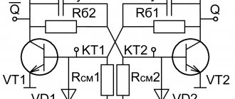
Assembling a current stabilizer from two transistors
In this circuit, the sensor functions are performed by resistor R2. Its value when connecting LEDs is selected using the formula:
0.6/In (load current).
An increase in In opens VT2, which, in turn, locks the transition of transistor VT1.
Experts consider a significant voltage drop across the main transistor to be a disadvantage of the circuit. There are no problems when connecting several LEDs. However, as the load increases, it is necessary to place VT1 on a large radiator to ensure effective ventilation of the working volume. Such solutions are used to create powerful chargers.