The bipolar power supply proposed by V. Oreshkin largely meets the mutually exclusive requirements for the UMZCH supply voltage stabilizer [1, 2]. This note describes a modified circuit that allows, by simple means, to increase the stabilization coefficient and reduce the output resistance while maintaining a small time constant of the aperiodic process. The modification came down to replacing ballast resistors in compensation stabilizers with current sources and taking into account the recommendations of Texas Instruments for constructing power supplies for UMZCH.
↑ Schematic diagram of the upgraded UMZCH power supply
The diagram of a bipolar power supply is shown in Fig. 1.
Fig.1. Bipolar power supply UMZCH
It consists of two galvanically unconnected rectifiers VD1, C1, C2, C5, C6, C9, C11, C13 and VD2, C3, C4, C7, C8, C10, C12, C14, two parametric stabilizers made on zener diodes VD3, VD4 and current sources on transistors VT5, VT6, and emitter followers on transistors VT1, VT3 and VT2, VT4. The stabilization coefficient is increased due to the supply of the reference voltage source of one stabilizer from the output voltage of the other and the use of current sources instead of resistors.
The rectifiers are assembled on diode bridges VD1, VD2, consisting of double Schottky diodes with a common cathode 16CTQ100. The diodes are connected in parallel.
Capacitors C1...C8; C9, C10 and RC - chains R9, C23 and R10, C24 are installed in accordance with the recommendations of Texas Instruments for the construction of power supplies for UMZCH [3].
To reduce noise, each zener diode VD3, VD4 is shunted by a pair of capacitors - oxide and film (C15, C17 and C16, C18, respectively).
Current sources on transistors VT5, VT6 contain parametric stabilizers HL1, C19, C21, R8 and HL2, C20, C22 in the bases of the transistors.
The current of each source is equal to: IVD4=(UHL1-UbeVT5)/R4=(1.76-0.56)/0.13=9.2 mA, IVD3=(UHL2-UbeVT6)/R7=9.2 mA.
Resistors R5, R6 reduce the power dissipated on the collectors of the current source transistors.
The collectors (cases) of powerful transistors VT1, VT2 are connected to the common wire of the power supply, which makes it possible to do without heat-conducting gaskets, thereby improving heat dissipation at high load currents.
To reduce the dynamic resistance of the power supply, its outputs are shunted with pairs of oxide-film capacitors (C25, C27 and C26, C28, respectively). Ballast resistors with green LEDs serve for indication (HL3, R11 and HL4, R12).
Resistor R2 is designed to trigger the bipolar stabilizer when the power is turned on.
The stabilizer has protection against short circuits in the load. If there is a short circuit in any arm, both stabilizers are switched off.
Main technical characteristics:
Stabilizer output voltage, V…. ±15 Maximum load current, A…. 20 Stabilization coefficient, not less than…. 1500 Output impedance, no more, Ohm.... 0.01 Voltage on the step-down windings of the power transformer, V.... 2×20
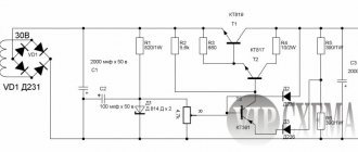
Powerful bipolar voltage stabilizer for UMZCH
The author offers a bipolar supply voltage stabilizer suitable for amplifiers with a power of up to 50-100 W per channel. The device is made of powerful field-effect transistors capable of operating under multiple short-term current overloads. The use of such stabilizers is largely justified in amplifiers with high sensitivity to changes and ripples in the supply voltage, which is especially characteristic of simple amplifiers without general feedback.
As you know, to power the powerful output stage of the UMZCH, a number of designs use a separate power source, and the rest of the amplifier is powered by a voltage stabilizer. Most of these power supplies are unstabilized and consist of two full-wave rectifiers (for voltages of positive and negative polarity) with a midpoint with smoothing capacitors. This unstabilized voltage is not used by the rest of the amplifier if it has additional nodes and a signal source switch (a complete, “integrated” amplifier). In addition, the general feedback used in most UMZCHs significantly reduces sensitivity to supply voltage ripples. And if the depth of the overall feedback is small or non-existent, supply voltage ripples can be heard through acoustic systems.
A fundamental way to suppress ripple and instability is to power the output stages of the amplifier with a stabilized voltage, however, the use of integrated stabilizers also encounters a number of problems. The fact is that such stabilizers have a relatively large voltage drop. In addition, they usually have built-in current and power limiters, which can generally negate the advantages of the stabilizer. You can, of course, use a high-power integrated stabilizer (for example, with an output current of 10 A), but its cost, in my opinion, is unacceptable. An alternative to solving this problem may be to use powerful field-effect transistors in the supply voltage stabilizer. These transistors, by the way, are inexpensive and have a low open-channel resistance (hundredths of an ohm) and a maximum current of up to 70 ... 100 A, which makes it possible to design stabilizers with a very low voltage drop (no more than 0.25 V) at a current of up to 20 A. Parameters of the described stabilizer are as follows. With an output voltage of 27 V, its maximum current reaches 4.5 A. With such a load current, the minimum operating voltage between input and output does not exceed 0.25 V. The difference between the output voltage of the stabilizer without load and the voltage at a load current of 4.5 A is no more than 0.15 V, at a current of 6 A this difference does not exceed 0.16 V. Such parameters of the stabilizer are ensured by the powerful field-effect transistors used in it - IRF4905 (p-channel) with a maximum drain current of 74 A and an open channel resistance of 0.02 Ohm and IRL2505 (p-channel), with a corresponding current of 104 A and a resistance of 0.008 Ohm.
Rice. 1
A bipolar stabilizer consists of two independent voltage sources of positive and negative polarity (Fig. 1). The upper part of the circuit refers to the positive polarity stabilizer, and the lower part refers to the negative polarity stabilizer. For ease of comparison, the numbering of the corresponding elements differs only in the prefixes 1 and 2. First, about some features of the stabilizer. It contains three critical elements - capacitors C2 and SZ and a zener diode VD1. The capacitance values of capacitors C2 and SZ indicated in the diagram are in a sense a compromise: when they are reduced, the possibility of self-excitation of the stabilizer arises. Increasing their capacitance to 1 µF leads to ripples, which are always present in the rectified voltage, penetrating the output of the stabilizer. Now a few words about why the VD1 zener diode (BZX55-C7V5) with a stabilization voltage of 7.5 V was chosen. It is advisable to choose a zener diode whose differential resistance is minimal (it affects the properties of the entire stabilizer). Of all the zener diodes in the BZX55 series, the zener diodes BZX55-C7V5 and BZX55-C8V2 have the lowest differential resistance (7 Ohms). If the input voltage of the stabilizer is less than 20...25 V, it is advisable to use a zener diode with a voltage of no more than 3.3 V (for example, BZX55-C3V3). The negative polarity stabilizer circuit with minor modifications was borrowed from [1] and was already used by me once to control the rotation speed of a drill (with a current reserve of 20...30 A). Compared to the circuit from [1], in the circuit in Fig. 1, the values of some capacitors and resistors were changed, a zener diode VD2 was added to protect the VT2 gate from breakdown, and a zener diode (VD1) was used for a different stabilization voltage (7.5 V). The positive polarity stabilizer circuit is a mirror image of the negative polarity stabilizer circuit. Instead of an n-channel one, it uses a p-channel field-effect transistor IRF4905 in a TO-220 (VT2) package; instead of a bipolar transistor of the pnp structure, a transistor of the npn structure is used. BC337-40 or KT503B (VT1), and the load of the parallel stabilizer DA1 (TL431CZ in the TO-92 package) is included in its anode circuit. Although this connection of the load is less known, it is most common in switching power supplies for computers. A few notes on how the described stabilizer can be modified for use with a supply voltage of +/-35...45 V. In this case, the resistance of resistor R4 (620 Ohms) must be increased to 0.9.. 1 kOhm so that the current through the stabilizer DA1 ( TL431CZ) did not exceed half of its maximum current of 50 mA. Instead of a complementary pair of transistors BC327/BC337 (Uke max = 45 V, Iktah = 0.8 A, PKmax = 0.6 W), you should use a pair with a slightly higher voltage Uke max. for example, 2SA1284/2SC3244 (UK3max = 100 V, lKmax = 0.5 A, PKmax = 0.9 W). It is advisable to install field-effect transistors on heat sinks with a large cooling area. It should also be added that to set the required stabilization voltage, you will need to change the values of resistors R5, R6 and R7. It is advisable to use a zener diode for a stabilization voltage of 7.5 V (BZX55-C7V5). I recommend purchasing the TL431CZ chip from National Semiconductor, Texas Instruments, Vishay, Motorola. All resistors, except for tuning R6 (SPZ-19A) have a power of 0.25 W, ceramic capacitors have a voltage of 50 V.
Rice. 2
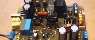
Since I needed two bipolar stabilizer boards (one for each channel of the UMZCH), using the Sprint Layout 5.0 program I laid out the printed circuit board (Fig. 2, printed its drawing on tracing paper intended for printing with a laser printer, and made it using the method described by me in [2, 3]. The appearance of the mounted board is shown in Fig. 3
Rice. 3
To test the operation of the stabilizer, I used three digital multimeters, two of which measured the input and output voltages of the stabilizer, and the third, in ammeter mode, measured its output current. Here it is necessary to add that the diagram in Fig. 4 was used to test a positive voltage stabilizer. The properties of a negative voltage stabilizer were tested in a similar way.
Rice. 4
A ceramic resistor SQP with a power of 20 W with a resistance of 1 Ohm was used as a load (R1), and a PE-75 resistor with a power of 75 W with a resistance of 5 Ohm was used as R2. Thus, the total load resistance (6 Ohms) of the stabilizer corresponded to a total power of 95 W. and the current is 4.5 A. When testing the stabilizer, I used a modified stabilized power supply unit B5-47 as a power source, in which the output voltage (up to 30 V) is provided at a load current of up to 4 5 A (up to 3 A without modification). To increase the current limit limit to 4.59 A, it is necessary to install jumpers in the remote control connector located on the rear wall of the unit between contacts 23, 24, 26 and 50, and on the front panel set the maximum current value to 2.99 A. The results of testing the operation of the stabilizers are complete confirmed their parameters. The stabilizers have a significant current reserve, and the load power of each stabilizer corresponds to 121.5 W, for a total of 243 W.
If the power of one amplifier channel is P = 35 W, and the load resistance is R = 4 Ohms, then the amplitude of the signal voltage U » 17 V and the current lm = 4.25 A. This means that if the stabilizer is bipolar and consists of stabilizers positive and negative polarity, each of them must provide a maximum current of 4.25 A. If the output voltage of the stabilizer is 27 V and the current in the load is 4.25 A, then the equivalent load corresponds to a resistance ReKB = 6.35 Ohms. That is why the load resistance of the stabilizer was chosen to be 6 ohms. During testing, a real power supply rectifier with a high current and a high ripple level was also used (storage capacitor with a capacity of 10000 μF and rectifier diodes DSS 60-0045V (Uobp = 45 V, lmax = 60 A, Upr = 0.35 V/10 A), connected via a bridge circuit.
The described stabilizer is also resistant to short-term overloads. I used it to adjust the rotation speed of a drill, in which the motor starting current reaches 20 A. Thus, the stabilizer has a significant current reserve, allowing it to be used with large heat sinks and in more powerful UMZCH. Now a few words about installing and adjusting the stabilizer in amplifier First of all, it is necessary to evaluate, using an oscilloscope, the minimum values of the supply voltage of the output stages of the UMZCH at maximum load. To do this, connect a resistor with a nominal value equal to the AC resistance (4 or 8 Ohms) and a power corresponding to the maximum for the UMZCH to the output of the UMZCH. Apply a signal with a frequency of 20...30 Hz from generator 34 to the input of the amplifier, and use the volume control to set the signal level corresponding to the maximum power amplifier Next, you need to determine the minimum absolute value (taking into account the ripple amplitude) of the supply voltages and set the stabilization voltage with trimming resistor R6 to approximately 1 V less than this minimum value in each of the stabilizers. Before installing two boards of such stabilizers in each of the channels in the amplifier (“Idol U-001”), I replaced the KD208A diodes (Unp = 1 V/1.5 A) in the bridge rectifiers of the power supplies with MBR10100 Schottky diodes (Unp = 0.45 V/1 .5 A) and KD209A diodes in a 30 V voltage stabilizer with HER503 diodes. In addition, the capacity of the smoothing capacitors was doubled (both in the rectifiers of the output stages and in the 30 V stabilizer).
After installing the stabilizers in the case and turning on the amplifier, it is necessary to check and adjust the balance of the output stages with respect to direct current, and then the quiescent current of powerful transistors. Having adjusted the operating modes of the transistors of the output stages of the UMZCH with installed stabilizers, I found a noticeable decrease in the background even at maximum sensitivity in the absence of an input signal.
Literature
1 Nechaev I. Powerful voltage stabilizer module on a field-effect transistor. - Radio, 2005, No. 2. p. 30. 31 2 Kuzminov A. Photo reproduction method for making a photomask of printed circuit boards at home. - Technologies in the electronic industry, 2010 No. 5-7 3 Kuzminov A. Manufacturing devices on printed circuit boards with high resolution at home. — Technologies in the electronic industry, 2010. No. 8-10
Author: A. Kuzminov, Moscow
↑ Parts and analogues
The parts list (BOM) is below.
Details:
VD1, VD2 Schottky diode 16CTQ100 IR (100V, 16A) - 8 pcs., VD3, VD4 Zener diode BZX55C16 (16V, 0.4W), glass - 2 pcs., HL1, HL2 LED FYL-3014HD red d= 3 mm - 2 pcs., HL3, HL4 LED BL-B2141Q G green.d=3 - 2 pcs., VT1 Transistor KT827A (20A; 100V), housing TO-3 - 1 pc., VT2 Transistor KT825A (20A; 100V), case TO-3 - 1 pc., VT3 Transistor BD140, case TO-126 - 1 pc., VT4 Transistor BD139, case TO-126 - 1 pc., VT5 Transistor 2SA1013, case TO-92mod - 1 pc., VT6 Transistor 2SC2383, TO-92mod housing - 1 pc., R1, R3 Resistor -0.25-3.3 kOhm - 2 pcs., R2 Resistor -2-470 Ohm - 1 pc., R4, R7 Resistor -0.25- 130 Ohm - 2 pcs., R5, R6 Resistor -0.25-220 Ohm - 2 pcs., R8 Resistor -0.25-9.1 kOhm - 1 pc., R9, R10 CHIP resistor F2512-1 Ohm, 1W 1% - 2 pcs., R11, R12 Resistor -0.5-2.7 kOhm - 2 pcs., C1...C8 Capacitor 0.1/250V K73-17 - 8 pcs., C9, C10, C23, C24 Capacitor CHIP 1812 0.1µF/100V X7R 10% - 4 pcs., C11...C14 Capacitor 10000/50V 3035+85°C - 4 pcs., C15, C16 Capacitor 47/63V 0611+105°C - 2 pcs., C17 …C20 Capacitor 0.1/63V K73-17 - 4 pcs., C21, C22 Capacitor 47/16V 0511+105°C - 2 pcs., C25, C26 Capacitor 470/35V 0820+105°C - 2 pcs. C27, C28 Capacitor 1/63V K73-17 - 2 pcs., Radiator for VT1, VT2 Printed circuit board 150×70×2 mm - 1 pc.
The power supply uses MLT or foreign MF output resistors with the power indicated on the circuit diagram (Fig. 1).
Capacitors C1 - C8, C17 - C20, C27, C28 type K73-17, imported oxide capacitors. Capacitors C17 - C20 can be replaced with better results with CBB21/MPP made of metallized polypropylene (for example, 0.15 µF, 100 V from the Datagorsk fair). For C27, C28, 1 µF, 100 V (Suntan, polyester) is suitable.
Transistors KT825A and KT827A can be replaced with composite ones (KT819G + KT815G and KT818G + KT814G), while the emitter junctions of powerful transistors KT819G and KT818G must be shunted with resistors with a resistance of 100 - 150 Ohms. It is possible to replace high-power composite transistors with MJ11032 and MJ11033. With a maximum load current of 5 - 7 A, transistors TIP142 and TIP147, as well as BDW42G BDW47G, are suitable.
Transistors VT1, VT2 are mounted on a heat sink with a cooling surface area of 900 sq. cm without heat-insulating gaskets using heat-conducting paste ALSIL-3.
Instead of transistors BD139 and BD140, 2SC3502 and 2SA1380 or BF471 and BF472 are suitable. When replacing, be sure to check the pinout of the transistors.
Transistors VT5, VT6 type 2SA1013, 2SC2383 can be replaced with domestic KT502E, KT503E; KT6116, KT6117 or imported 2N5401, 2N5551; 2SA1145, 2SC2705 and others.
Schottky diodes in bridges VD1, VD2 are replaceable with MBR20200CTG (200 V, 10 A) with a common cathode, or with SR10100 (10 A, 100 V, TO-220-2). In the latter case, the printed circuit board will need to be adjusted.
For consumption currents of more than 2 A, it is necessary to equip the diodes with small radiators and (or) provide them with fan cooling.
With relatively low current consumption (up to 2 A) in diode bridges, you can use high-performance diodes HER505 (5 A, 1000 V), ultra-fast diodes SF56 (5 A, 400 V) or ultrafast STTH5R06FP (5 A, 600 V, TO-220- 2).
The maximum voltage stabilizer current is determined by the power transformer. For example, in the one shown in Fig. In diagram 1, transformer T1 type TPP321 provides a maximum current of no more than 4 A.
Water-cooled bipolar voltage regulator
Compensating voltage stabilizers of continuous action of the series type have low efficiency, but a high stabilization coefficient and low output resistance. That's why they are still widely used. However, they are characterized by low reliability when overloaded or shorted in the load. This is especially dangerous for transistor devices, so it is necessary to introduce complex protection units with current sensors into the stabilizers. In the powerful bipolar voltage regulator discussed in this article, the output current is limited. The device is not afraid of overloads and can operate on high-capacity filter capacitors.
Analysis of UMZCH circuits allows us to conclude that continuous voltage stabilizers are rarely used to power their output stages. The reasons for this are the high cost of such stabilizers, large energy losses when using them, and most importantly - “it will do as is”, because it works without a stabilizer.
When there is no stabilizer, the amplifier supply voltage varies depending on the load over a wide range (in the Pioneer-714 AV receiver - 30...50 V). The fact is that the average output voltage of a rectifier with a capacitive filter strongly depends on the load current. Moreover, the filter capacitors are charged by pulses in each half-cycle of the mains voltage. The process may take several half-cycles, and this is partially transferred to the UMZCH load.
In amateur radio literature, the opinion has been repeatedly expressed about the need to power the UMZCH from a stabilized source to ensure a more natural sound. Indeed, at the maximum output power of the amplifier, the range of voltage ripples from an unstabilized source reaches several tens of volts. This is imperceptible at the peak values of high-frequency components of audio signals, but it affects the amplification of their high-level low-frequency components, the peaks of which have a long duration. As a result, the filter capacitors have time to discharge, the supply voltage decreases, and hence the peak output power of the amplifier. If the decrease in supply voltage is such that it leads to a decrease in the quiescent current of the amplifier's output transistors, this can cause additional nonlinear distortion.
The fundamental way to suppress ripple and instability of the supply voltage is to stabilize it. The stabilizer reduces voltage ripple on the power lines by one or two orders of magnitude, which makes it easy to obtain the maximum amplitude of the amplifier's output signal. In addition to reducing the background level with a frequency of 50 (100) Hz, nonlinear distortions and the likelihood of signal clipping at loudness peaks are also reduced. The margin for the maximum permissible parameters of the amplifier output stage transistors increases. The likelihood of network interference penetrating the amplifier output is reduced.
In addition, the use of a stabilizer makes it possible to simplify the amplifier, which has a beneficial effect on the sound. Another plus is that the function of protecting the amplifier output stage from overload can also be entrusted to the stabilizer.
Of the minuses, the implementation of a powerful and reliable continuous voltage stabilizer becomes a significant financial problem and a technically difficult task. In addition, there is a need to remove a large amount of heat from the power transistors of the stabilizer. The total efficiency and power dissipation of an amplifier together with a stabilizer are much worse than without it.
To improve the quality of the power source, it is advisable to use a network transformer with reduced induction. As is known, the inrush current of conventional transformers reaches values significantly exceeding the operating current. Reducing the induction amplitude in the magnetic circuit by half significantly increases reliability, reduces the dissipation flux of the transformer and reduces its starting current to a value not exceeding the rated no-load current. However, lower induction leads to an increase in the required number of winding turns and, as a consequence, to a deterioration in the weight and size parameters of the transformer, its cost and an increase in energy losses due to the active resistance of the windings. But we are talking about truly high-quality sound reproduction, right? And the sound of an amplifier powered by a stabilized voltage is significantly better compared to the sound of the same amplifier without a stabilizer.
A bipolar voltage stabilizer, the circuit of which is shown in the figure , is designed to power the UMZCH.
Main technical parameters
- Number of stabilization channels….2
- Output voltages, V….+41 and -41
- Maximum load current of each channel, A....4
- Ripple range at load current 4 A, mV ....4.7
- Power dissipation at maximum load current, W….180
It consists of two independent voltage stabilizers of positive and negative polarity relative to the common wire. The upper part of the circuit refers to the positive polarity stabilizer, and the lower part refers to the negative polarity stabilizer. The negative polarity stabilizer circuit is essentially a mirror image of the positive polarity stabilizer circuit. Therefore, we will consider in detail only the voltage stabilizer of positive polarity.
The alternating voltage removed from winding II of transformer T1 rectifies a full-wave rectifier using dual Schottky diodes VD3 and VD4 SR30100P, which have an insulated housing, so it is convenient to mount them on a common heat sink.
Through the noise-suppressing choke L1, the rectified voltage is supplied to smoothing and noise-suppressing capacitors C8-C16 and then to the equalizing emitter currents of parallel-connected transistors VT1-VT9 and resistors R3-R11. These resistors have a fairly high resistance, which contributes to the effective “isolation” of the collector circuits of transistors VT1 - VT9 from network noise.
Together with transistor VT20, transistors VT1-VT9 form a powerful composite transistor with a high current gain. The base current of transistor VT20 flows into the collector of transistor VT22. Transistor VT22 is controlled by voltage from the output of op-amp DA3.1.
Zener diodes VD13, VD14 connected in series are connected to the output of the stabilizer, the total stabilization voltage of which serves as a reference voltage for the stabilizer in question. Instead of zener diodes, you can install a resistor of such resistance that, together with resistor R29, it provides zero potential at the point of their connection at the rated output voltage of the stabilizer. But compared to zener diodes, this is a less effective option. The potential shifted by zener diodes or a resistor in the stabilization system represents a mismatch signal and is supplied to the inverting input of the op-amp DA3.1, the non-inverting input of which is connected to the “0” wire.
Keep in mind that the “0” and “Common” wires must be connected to each other and to the common wire of the device (amplifier) powered by the stabilizer on the latter’s board. This significantly reduces the level of interference and interference in the stabilized voltage. Resistor R21 ensures the operation of the stabilizer when no amplifier is connected to it.
During operation, the op-amp continuously compares the potential at its inverting input with the zero potential at the non-inverting input. Next, he controls the transistor VT22, and with it the composite transistor VT20, VT1-VT9, so that the specified voltage is maintained at the output of the stabilizer.
Suppose the voltage at the stabilizer output decreases due to an increase in load current. The potential at the inverting input of the op-amp DA3.1 will become negative relative to the non-inverting one, and the voltage at the output of the op-amp will increase. This will lead to an increase in the collector current of transistor VT22, and with it the base and emitter current of transistor VT20. As a result, the total collector current of transistors VT1-VT9 will increase, compensating for the increase in load current. The output voltage will return to its previous value.
The soft start device on transistor VT19 and relay K1 ensure a smooth increase in voltage across the battery of capacitors C28-C30, C34-C63 when the stabilizer (primary winding of transformer T1) is connected to the network. At this moment, current begins to flow through resistor R2, charging capacitor C27. When, after 30...35 s, the voltage applied to the zener diode VD9 reaches 36 V, it opens. This leads to the opening of transistor VT19 and activation of relay K1, which switches resistors that limit the output current of the stabilizer.
Until the relay is triggered, this current is limited by resistor R32 to 450...650 mA, which eliminates the surge charging current of the battery of capacitors C28-C30, C34-C63 with a total capacity of more than 100,000 µF. The triggered relay connects resistor R35 in parallel with resistor R32. From this moment on, the stabilizer can supply a current reaching 4 A to the load.
If the output of the stabilizer is accidentally shorted to the common wire, the current will also not exceed 4 A, but the power dissipated by transistors VT1-VT9 will increase sharply. However, it will not exceed 25 W per transistor. It follows from this that the voltage stabilizer is reliable and is not afraid of short circuits in the load.
To accurately set the current limit levels, it is necessary to temporarily replace resistor R32 with a variable resistor with a resistance of about 500 kOhm, and leave resistor R35 uninstalled. Move the variable resistor slider to the maximum resistance position. Having closed the stabilizer output with an ammeter, turn on the stabilizer and gradually reduce the resistance of the variable resistor, observing the ammeter readings. When the required safe starting current is reached, turn off the stabilizer, measure the introduced resistance of the variable resistor and replace it with a constant resistor of the same resistance.
Then, instead of resistor R35, connect a variable resistor with a resistance of 100 kOhm, and connect the maximum load to the output of the stabilizer through an ammeter. Turn on the stabilizer and wait for the relay to operate. After this, begin to gradually reduce the resistance of the variable resistor. When the rated stabilization voltage and the specified maximum load current are reached, turn off the stabilizer, measure the introduced resistance of the variable resistor and replace it with a constant one.
The same procedure must be performed with a negative voltage stabilizer. You cannot simply install resistors R33 and R36 of the same resistance as R32 and R35, respectively. The fact is that the current transfer coefficients of the transistors used in both stabilizers differ significantly. For example, for 2SA1943 transistors it is about 140, and for 2SC5200 it is only 85.
Transformers T1 and T2 are custom-made with low induction and secondary windings at 2x54 V (with middle terminals) with a load current of 5 A. The transformers are installed each on their side in the very bottom part of the heat exchanger (aqua block) of the stabilizer water cooling system. The water block serves as a kind of chassis on which all the components of the device are located. Before installing the transformers, ideally flat landing pads are molded for them using epoxy resin. Then the transformers are pressed against the water block using M12 threaded rods.
In idle mode, the voltage at the outputs of the rectifiers (inputs of the stabilizers themselves) is 76 V. When connected to the output of a load stabilizer with a resistance of 10 Ohms, it drops to 64 V. If a higher load current is required, for example 10 A, then the values of resistors R3-R20 should be reduced up to 10 ohms.
Suppressor diodes VD1 and VD2 are designed to suppress overvoltages during transient processes accompanying the inclusion of the stabilizer in the network.
With proper installation and assembly, the stabilizer starts working without any problems. With a continuous load of 4 A current, transistors VT1 - VT9 dissipate about 60 W of power (6 W for each transistor). Each of the resistors R3-R11 has 4 W. Together, voltage stabilizers of positive and negative polarity dissipate about 180 W. Two pairs of stabilizers for powering the amplifiers of the left and right stereo channels, installed on a common water block, dissipate 360 W.
The water block consists of two pieces of duralumin tire with a cross-section of 100×10 mm and a length of 1000 mm, tightened with screws along the perimeter. Automotive sealant was used to seal the joint between the tires. On the inner surface of each tire, two parallel grooves measuring 960x15x4 mm are milled, through which cooling water flows. The total cross-section of the water supply channel is 15x8 mm, its total length is 1920 mm, water flow is 0.75 l/min, the water temperature at the inlet of the water block is 24°C, at the outlet - 29°C. Water comes from the water supply through a single-stage filter.
Four years of experience in operating such an open water cooling system has shown the stability of its thermal parameters. But the system can also be made closed with the circulation of distilled water through an aqua block and an external car radiator.
Transistors VT1—VT18 are mounted on a printed circuit board with an aluminum substrate, pressed to the aquablock using thermal conductive paste. The board surface temperature is about 34°C. Transistors 2SA1943 and 2SC5200 heat up to a temperature of about 50°C. Tests showed that this temperature remained unchanged for three hours of operation.
The described cooling system is compact, efficient and absolutely silent. It allows you to remove about a kilowatt of thermal power. As a signaling device for the emergency absence of running water in the system, a pressure sensor DRD-40 is installed in the supply pipeline. It is ideal for standard plumbing. In the event of an emergency water shutdown, the contacts of this sensor open and disconnect the stabilizer from the electrical network.
In addition, it is necessary to install temperature sensors on one or more 2SA1943 transistors, which, as practice has shown, heat up more than 2SC5200 transistors. It is recommended to install the same sensors on transformers.
Author: V. FEDOSOV, Krasnodar
↑ Printed circuit board
The parts of the device, except for the power transformer T1 and powerful transistors VT1, VT2, are mounted on a printed circuit board measuring 150x70 mm (see Fig. 2), made of foil fiberglass laminate.
Rice. 2. Placement of parts on the printed circuit board. The tracks are shown “in the light”, smd elements C9, C10, C23, C24, R9, R10 are installed on the side of the printed tracks
It is advisable to additionally solder the “power” tracks on the printed circuit board on top with tinned mounting wire with a diameter of 0.5 - 0.7 mm.
↑ Conclusions
The use of two separate rectifier bridges in the device, in my opinion, is a disadvantage, since compared to one diode bridge we have a twice as high voltage drop across the rectifier diodes, therefore, a lower maximum power.
In addition, the design with two diode bridges has large dimensions. The presence of two independently operating secondary windings of the transformer puts forward the additional requirement that their output voltages be equal.
The only advantage of a circuit with two rectifier bridges is that the maximum voltage on the bridge diode is two times lower, which can play a positive role when choosing Schottky rectifier diodes that have a low reverse voltage, no more than 45 - 200 V.
The described device can be used not only as a power source for UMZCH, but also as a powerful power source for automation devices.
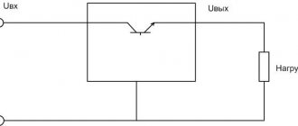
Transistor voltage stabilizer
- Stabilizer on one zener diode
- Stabilizer on one transistor
- Transistor stabilizer with short circuit protection
- Stabilizer with adjustable output voltage
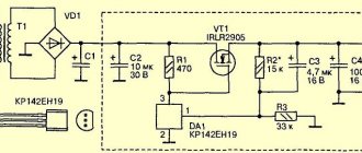
Stabilizer on one zener diode
To smooth out voltage ripples and constant current at the output of the power supply, stabilizers are used.
As a rule, the stabilizer is based on a zener diode. Zener diode is a semiconductor device with voltage stabilization properties. Unlike a conventional diode, it operates in reverse polarity (plus is supplied to the cathode), in avalanche breakdown mode. Due to this property of the zener diode, the voltage on it, and therefore on the load, practically does not change. The figure below shows a diagram of a simple stabilizer. This stabilizer is suitable for powering low-power devices.
The principle of operation of the stabilizer on a zener diode
A capacitor is needed to smooth out voltage ripples; it is called a filter. A resistor is needed to smooth out current ripples and is called a damping resistor. The zener diode stabilizes the voltage across the load. For normal operation of this circuit, the supply voltage must be greater than 40...50%. The zener diode should be selected for the voltage and current we need.
Stabilizer on one transistor
To power a higher power load, a transistor is added to the circuit. An example circuit is shown below.
The principle of operation of a stabilizer on a single transistor
The chain of R1 and VT1 is already familiar to us from the previous circuit; this is the simplest stabilizer; it sets a stabilized voltage based on transistor VT2. The transistor, in turn, performs the function of a current amplifier and is a control element in this circuit. For example, as the input voltage increases, the output voltage will tend to increase. This leads to a decrease in the voltage at the emitter junction of transistor VT2, which leads to its closure. In this case, the voltage drop in the emitter-collector section increases so much that the voltage on the zener diode decreases to the original level. When the voltage drops, the stabilizer reacts in the reverse order.
Transistor stabilizer with short circuit protection
In the practice of a radio amateur, mistakes occur and a short circuit occurs. To reduce the consequences of a short circuit, consider a stabilizer circuit for two fixed voltages and with short circuit protection.
As you can see, transistor V4, diodes V6 and V7 have been added to this circuit, and a parametric stabilizer consisting of resistor R1, diodes V2, V3 is equipped with switch S2.
Operating principle of stabilizer protection
This circuit is designed for a short-circuit response current of 250...300 mA; as long as it is not exceeded, the current will pass through a voltage divider consisting of diode V7 and resistor R3. By selecting this resistor, you can adjust the protection threshold. Diode V6 will be closed and will not have any effect on the work. When the protection is triggered, diode V7 will close, and diode V6 will open and bypass the zener diode connections, while transistors V4 and V5 will close. The load current will drop to 20...30 mA. Transistor V5 should be installed on the heat sink.
Stabilizer with adjustable output voltage
When repairing or adjusting electronic devices, it is necessary to have a power supply with an adjustable output voltage. A schematic diagram of voltage-regulated stabilizers is presented below.
The principle of operation of a stabilizer with voltage regulation
A parametric stabilizer consisting of R2 and V2 stabilizes the voltage across the variable resistor R3. The voltage from this resistor is supplied to the control transistor. This transistor is connected according to the emitter follower circuit, the load of which is resistor R4. The voltage from resistor R4 is supplied to the control transistor V4, the load of which is already our powered device. Voltage regulation is carried out by variable resistor R3; if the resistor slider is in the minimum position according to the circuit, then the voltage to open transistors V3 and V4 is not enough and the output will have a minimum voltage. When the engine rotates, the transistors begin to open, which increases the voltage across the load. As the load current increases, the voltage drop across resistor R1 and lamp H1 begins to light up; at a current of 250 mA, a dim glow is observed, and at a current of 500 mA and above, a bright glow is observed. Transistor V4 should be installed on the heat sink. With an increased load of more than 500 mA, you should turn off the power supply as quickly as possible, since under prolonged maximum load the diodes in the rectifier bridge and transistor V4 fail.
These circuits, when assembled correctly, do not require adjustment. They can also be upgraded to higher currents and voltages. By selecting radioelements with the parameters we need.
That's all. If you have comments or suggestions regarding this article, please write to the site administrator.
Good luck!
↑ Sources mentioned
1. Oreshkin V. Power stabilizer UMZCH // Radio, 1987, No. 8, p.
31. 2. A modified version of a low-noise bipolar power supply (see comments 32-36 to the article.) 3. Recommendations from Texas Instruments for constructing power supplies for UMZCH. Thank you for your attention!