Have a good time everyone. Let me introduce a power inverter for powering a powerful audio amplifier. Unfortunately, there are few such projects on the Internet, especially well-replicated ones. Therefore, it was decided to make such a power source from scratch. It took a lot of time to design, build and test this UPS. And now, having carried out the last tests (all tests were successful), we can say that the project is completed and it can be presented to the respected amateur radio audience of the site 2 Schemy.ru
The project of this inverter is excellent for UMZCH on 2x TDA7294, in fact, it was developed for it. The converter is not complicated and should be successfully assembled by not very advanced electronics engineers. You don't even need an oscilloscope to run it, but of course it would be useful. The basis of the power supply circuit is m/s TL494.
It is short circuit protected and should provide 250W of continuous power. The converter also has an additional output voltage of +/- 9..12 V, which will be used to power the preamplifier, fans, etc.
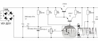
Switching power supply for an amplifier - circuit diagram
The converter is made in accordance with this scheme. Board dimensions 150×100 mm.
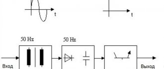
The inverter consists of several basic modules found in most similar power supplies, such as an ATX power supply. The fuse, thermistor and line filter consisting of C21, R21 and L5 go to the 220V AC power supply. Then the rectifier bridge D26-D29, inverter input capacitors C18 and C19 and power transistors Q8 and Q9 to switch the voltage at the transformer. Power transistors are controlled using an additional transformer T2 by one of the most popular PWM controllers - TL494 (KA7500). Current transformer T3 for measuring output power is connected in series with the primary winding. Transformer T1 has two separated secondary windings. One of them generates a voltage of 2×35 V, and the other 2×12 V. On each of the windings there are fast diodes D14-D17 and D22-D25, which in total form 2 rectifier bridges.
After loading the +/- 34 V line with a 14 ohm resistor, the voltage drops to +/- 31 V. This is a pretty good result for such a small ferrite core. After 5 minutes, diodes D22-D25, the main transformer and MOSFET heated up to a temperature of about 50C, which is quite safe. After connecting two channels of TDA7294, the voltage dropped to +/- 30 V. The inverter elements heated up like a resistive load. After experiments, the output circuit is equipped with 2200uF capacitors and 22uH/14A chokes. The voltage drop is slightly higher than in the case of 6.8uH, but their use clearly reduces the heating of the MOSFETs.
Output voltage under load of both outputs with 20 W bulbs:
Operating principle of a switching power supply
The 220 V voltage is rectified by a bridge with diodes D26-D29. The input capacitors C18 and C19 charge to a total voltage of 320V, and since the inverter operates in a half-bridge system, they divide them in half, resulting in 160V per capacitor. This voltage is further balanced by resistors R16 and R17. Thanks to this separation, it is possible to connect transformer T1 to one channel. The potential between the capacitors is then treated as ground, one end of the primary winding is connected to +160 V, the other to -160 V. The switching voltage of the primary winding of transformer T1 is carried out using a variable N-MOSFET transistor Q8 and Q9.
Capacitor C10 and the primary winding of current transformer T3 are located in series with the primary winding. The coupling capacitor is not needed for the operation of the circuit, but it plays a very important role - it protects against unbalanced energy consumption from the input capacitors and, therefore, before charging one of them to more than 200 V. The current transformer T3, also located in series with the primary winding, acts as short circuit protection. The current transformer provides galvanic isolation and allows you to measure the current value, reduced to the accuracy of its transmission. Its task is to inform the controller about the amount of current flowing through the primary winding T1.
In parallel with the primary winding of the main transformer there is a so-called pulse suppression circuit, which is formed by C13 and R18. It suppresses voltage surges generated when switching power transistors. They are not harmful to MOSFETs because their built-in diodes effectively protect against drain overvoltage. However, voltage surges can negatively affect the efficiency of the inverter, so it is important to eliminate them.
The power MOSFETs cannot be driven directly from the controller due to the change in the potential of the upper transistor source. The transistors are controlled using a special transformer T2. This is an ordinary pulse transformer operating in push-pull mode, opening power transistors. The control transformer T2 has at the input a set of voltage control elements on the windings, which, in addition to generating the voltage dictated by the controller, protect against the occurrence of core demagnetizing voltage. An uncontrolled demagnetization voltage would keep the transistor open. The elements directly responsible for eliminating the demagnetization voltage are diodes D7 and D9, as well as transistors Q3 and Q5. During idle time, when both MOSFETs are off, current flows through D7 and Q5 (or D9 and Q3) and maintains the demagnetization voltage around 1.4 V. This voltage is safe and cannot open the power transistor.
Voltage oscillogram at MOSFET inputs:
On the oscillogram you can clearly see the moment when the core stops being demagnetized by diodes D7 and D8 (D6 and D9) and begins to be magnetized in the opposite direction by transistors Q3 and Q4 (Q2 and Q5). During the core demagnetization phase, the voltage at the T2 gate reaches 18 V, and during the magnetization phase it drops to approximately 14 V. Why is one of the IR type drivers not used? First of all, the control transformer is more reliable, more predictable. IR drivers are very capricious and error prone.
An alternating voltage is generated on the secondary winding of the main transformer T1, so it needs to be rectified. The role of the rectifier is played by rectifying fast diodes, generating a symmetrical voltage. The output chokes are located behind the diodes - their presence affects the efficiency of the inverter, suppressing the surges that charge the output capacitors when one of the power transistors is turned on. Next are the output capacitors with preload resistors, which prevent the voltage from rising to too high values.
Practical Technique for Measuring Common Mode Interference
Special, especially certified equipment for measuring common mode interference is not always available to the engineer when examining power supply layouts during the design phase. However, more accessible tools, such as a digital oscilloscope, can be used to roughly estimate interference levels in the relatively low frequency region. The idea is to digitize the voltage waveforms across the test resistors, which are periodic signals, and then calculate their harmonic content through a Fourier transform.
In Fig. Figure 2 shows voltage oscillograms Umeas1 and Umeas2 relative to grounding (according to Fig. 1) for the RCA300.10240A unit [2] with the following parameters: Vin = 60 V, Vo = 24 V, Io = 1.25 A. This unit is powered from a DC network voltage, but includes a common mode noise filter. It also shows the spectral composition of the measured signals, calculated using the Fourier transform to a frequency equal to half the sampling frequency of the digitized signal (in this case, up to 12.5 MHz).
Rice. 2. Oscillograms and spectral composition of common mode interference of the RCA300.10240A block
In Fig. 2 shows the limiting curve for Class A in black, and in blue for Class B. As can be seen from the figure, the most critical range from the point of view of meeting the requirements of the standard is the first five harmonics of the conversion frequency (however, the first harmonic, just above 100 kHz, does not fall within still in the frequency range of interest to us). It should be noted that the difference in the oscillograms and spectra of signals recorded at different terminals of the block is due to the absence of a differential noise filter in its composition, so that the differential noise signal in the first case (oscillogram on the left) is subtracted from the common-mode noise signal, and in the second case ( right) stacks with it. However, in both cases, the block does not meet the requirements for Class B, but “passes” Class A.
Pulse IP controller
The controller is the basis of the inverter, so we will describe it in more detail. The inverter uses a TL494 controller with a set operating frequency the same as in ATX power supplies, that is, 30 kHz. The inverter does not have output voltage stabilization, so the controller operates with a maximum duty cycle of 85%. The controller is equipped with a soft start system consisting of elements C5 and R7. After starting the inverter, the circuit provides a smooth increase in the duty cycle starting from 0%, which eliminates the charging surge of the output capacitors. The TL494 can operate from 7 V, and this voltage supplying the buffer of the control transformer T2 causes the generation of a voltage at the gates of the order of 3 V. Such not fully open transistors will output tens of volts, which will lead to huge power losses and there is a high probability of exceeding the dangerous limit. To prevent this, protection is provided against too high a voltage drop. It consists of a resistor divider R4 - R5 and transistor Q1. After the voltage drops to 14.1 V, Q1 discharges the soft start capacitor, thereby reducing the charge to 0%.
Another function of the controller is to protect the inverter from short circuit. Information about the primary winding current is obtained by the controller through the current transformer T3. The current in the secondary winding T3 flows through resistor R9, across which a small voltage drops. Information about the voltage on R9 is sent via potentiometer PR1 to the error amplifier TL494 and compared with the voltage of the resistor divider R1 and R2. If the controller detects a voltage higher than 1.6 V on potentiometer PR1, it turns off the transistors before they cross the dangerous limit and is latched through D1 and R3. The power transistors remain off until the inverter is restarted. Unfortunately, this protection only works correctly on the +/- 35 V line. The +/- 12 V line is much weaker and in the event of a short circuit there may not be enough current for the protection to operate.
The controller's power supply is transformerless using capacitor resistance. The two capacitors C20 and C24 consume reactive energy from the mains and hence by causing current to flow, they charge the filter capacitor C1 through the rectifier D10-D13. Zener diode DZ1 protects against too high voltage on C1 and stabilizes them at 18 V.
Pulse transformers in power supply
The quality and performance of a pulse transformer affects the efficiency of the entire converter and the output voltage. However, the transformer not only performs the function of converting electricity, but also provides galvanic isolation from the 220 V network and thus has a great impact on safety.
Here's how to make such a transformer correctly. First of all there must be a ferrite core. It cannot have an air gap; its halves must fit perfectly together. Theoretically, a toroidal core can be used here, but making good insulation and winding will be quite difficult.
We recommend taking the main ETD34, ETD29 as a last resort, but then the maximum continuous power will be no more than 180 W. They don't cost much, so the best solution is to get a damaged ATX power supply. Burnt PC power supplies, in addition to all the necessary transformers, contain many more useful elements, including a surge protector, capacitors, diodes, and sometimes TL494 (KA7500).
Transformers must be carefully desoldered from the ATX power supply board, preferably using a hot air gun. After desoldering, do not try to disassemble the transformer because it will break. The transformer should be placed in water and boiled. After 5 minutes, you need to carefully grab the core halves through the fabric and separate them. If they don't want to separate, don't pull too hard - you'll break them! Place back and cook for another 5 minutes.
The process of winding the main transformer should begin with counting the amount of wire that will be wound. Due to the constant operating frequency and the specified maximum induction, the number of primary windings depends only on the cross-sectional area of the main ferrite core column. The maximum induction is limited to 250 mT due to half-bridge operation - here the magnetization asymmetry is simple.
Formula for calculating the number of turns:
n = 53 / Qr,
- where n is the number of windings of the primary winding,
- Qr is the cross-sectional area of the main core rod, given in cm2.
Thus, for a core with a cross-section of 0.5 cm2, you need to wind 106 turns, and for a core with a cross-section of 1.5 cm2, you will only need 35. Remember, do not wind half a turn - always round up to one plus. Calculating the number of secondary windings is the same as for any other transformer - the ratio of the output voltage to the input voltage is exactly equal to the ratio of the number of secondary windings to the number of primary windings.
The next step is to calculate the thickness of the winding wires. The most important thing to consider when calculating the thickness of the wires is the need to fill the entire core window with wire - this determines the magnetic connection of the transformer windings, and, consequently, the output voltage drop. The total cross-section of all wires passing through the core window should be about 40-50% of the cross-section of the main window (the main window is where the wire passes through the core). If this is your first time winding a transformer, you should get closer to this 40%. The calculations must also take into account the currents flowing through the cross-section of the windings. Typically the current density is 5 A/mm2 and this value should not be exceeded, the use of lower current densities is desirable. In the simulation, the primary side current is 220 W / 140 V = 1.6 A, so the wire cross-section should be 0.32 mm2, which means its thickness will be 0.6 mm. On the secondary side, a current of 220W/54V would be 4.1A, resulting in a cross-section of 0.82mm and an actual wire thickness of 1mm. In both cases, the maximum voltage drop during loading was taken into account. It should also be remembered that due to the skin effect of pulse transformers, the thickness of the wire is limited by the operating frequency - in our case at 30 kHz the maximum wire thickness is 0.9 mm. Instead of a 1mm thick wire, it is better to use two thinner wires. After calculating the number of coils and wires, check whether the calculated filling of the copper window corresponds to 40-50%.
Useful: High-quality headphone amplifier using op-amps and field-effect transistors
The primary winding of the transformer must be placed in two parts. The first part of the primary (of 35 turns) is wound like the first, on an empty frame. It is necessary to maintain the direction of the winding towards the frame - the second part of the winding must be wound in the same direction. After winding the first part, you need to solder the other end to an adapter, shortened pin, which is not included in the board. Then apply 4 layers of insulation tape on the winding and wind the entire secondary winding - this means the winding method. This improves the symmetry of the windings. The following +/- 12V secondary winding can be wound directly onto the +/- 35V winding in areas where a small amount of free space has been saved, and then completely insulated with 4 layers of electrical tape. Of course, it is also necessary to insulate the places where the ends of the windings are driven to the housing pins. As the last winding, wind the second part of the primary winding, always in the same direction as the previous one. After winding, you can insulate the last winding, but it is not necessary.
When the windings are ready, fold the core halves. The best and proven solution is to connect it with electrical tape and a drop of glue. We wrap the core with insulating tape several times.
The control transformer is made like any other pulse transformer. A small EE/EI obtained from ATX power supplies can be used as the core. You can also buy a TN-13 or TN-16 toroidal core. The number of windings depends, as usual, on the cross-section of the core.
In the case of toroids, the formula is:
n = 8 / Qr,
- where n is the number of windings of the primary winding,
- Qr is the cross-sectional area of the core, given in cm2.
The secondary windings should be wound with the same number of turns as the primary windings, only minor deviations are allowed. Since the transformer will only drive one pair of MOSFETs, the thickness of the wire is not important, its minimum thickness is less than 0.1 mm. In this case 0.3 mm. The first half of the primary winding must be wound in series - insulating layer - first secondary winding - insulating layer - second secondary winding - insulating layer - second half of the primary winding. The direction of the winding of the windings is very important, here the MOSFETs must be turned on one by one, and not simultaneously. After winding, we connect the core in the same way as in the previous transformer.
The current transformer is similar to the above. The number of coils here is arbitrary; in principle, the number of windings of the secondary winding is sufficient:
n = 4 / Qr,
- where n is the number of windings of the secondary winding,
- Qr is the cross-sectional area of the core circumference, given in cm2.
But since the currents here are very small, it is always better to use a larger number of turns. On the other hand, it is more important to maintain the appropriate ratio of the number of turns of both windings. If you decide to change this ratio, you will have to adjust the value of resistor R9.
Here is the formula for calculating R9 depending on the number of turns:
R9 = (0.9Ω * n2) / n1,
- where n2 is the number of windings of the secondary winding,
- n1 – number of windings of the primary winding.
With R9 changed, C7 also needs to be changed accordingly. The current transformer is easier to wind on a toroidal core, we recommend TN-13 or TN-16. However, you can make a transformer with an Sh-core. If you wind a transformer on a toroidal core, first wind the secondary winding with a large number of turns. Then insulating tape and, finally, the primary winding with 0.8 mm thick wire.
Add a link to a discussion of the article on the forum
RadioKot >Schemes >Power supply >Power supplies >
| Article tags: | Add a tag |
200 W switching power supply for UMZCH
Author: Alexey Malyshev Published 09/06/2012 Created with the help of KotoEd. Participant of the Competition “Congratulate the Cat as a Human Being 2012!”
Hello dear Cat! Happy birthday to you and all the best, so to speak! And as a gift, accept such a very useful thing as a power supply for an amplifier.
ATTENTION!
Some elements of this device are exposed to life-threatening mains voltage! Some elements retain a dangerous electrical charge after the device is unplugged! Therefore, when installing, setting up and working with the device, it is necessary to comply with electrical safety requirements. By repeating the device, you act at your own peril and risk. I, the author, do NOT bear any responsibility for any moral and material damage, damage to property, health and life caused as a result of repetition, use or inability to use this design.
So, let's begin.
Disputes about whether a switching power supply is good or bad for UMZCH (hereinafter referred to as SMPS) are beyond the scope of this article. Personally, I believe that a properly designed, soldered and adjusted SMPS is no worse (and in some respects even better) than a classic power supply with a network transformer.
In my case, the use of SMPS was necessary because I wanted to fit my amplifier into a flat case.
Before developing this SMPS, I studied many ready-made circuits available on the Internet and in the literature. Thus, among radio amateurs, different versions of the unstabilized SMPS circuit on the IR2153 chip are very popular. The advantage of these schemes is only one – simplicity. As for reliability, it is nonexistent - the IC itself does not have overload protection and soft start functions for charging output electrolytes, and the addition of these functions deprives the SMPS of its advantage - simplicity. In addition, the implementation of a soft start on this IC is extremely doubtful - it does not allow changing the pulse width, and methods based on changing the operating frequency of the IC are ineffective in a “regular” half-bridge SMPS and are applicable in resonant converters. I somehow didn’t really want to blast electrolytes and keys with huge currents when turning on the unit.
The possibility of using the well-known TL494 IC was also considered. However, upon deeper study, it turned out that for reliable operation around this IC you will have to hang a bunch of all sorts of transistors, resistors, capacitors and diodes. And this is no longer “our method”
As a result, the choice fell on a more modern and faster chip called UC3825 (Russian analogue of K1156EU2). A detailed description of this IC can be found in its Russian datasheet [1] and in the Radio magazine [2].
For those who are too lazy to read these sources, I will say that this is a high-speed PWM controller with the following capabilities:
- Control of powerful MOS transistors.
- Work in devices with voltage and current feedback.
- Operation at frequencies up to 1 MHz.
- The delay of the signal passing through the circuit is 50ns.
- Half-bridge outputs for current up to 1.5A.
- Wideband error amplifier.
- Presence of PWM latch.
- Current limitation in each period.
- Smooth launch. Limitation of the maximum output pulse duration.
- Undervoltage protection with hysteresis.
- Switching off the circuit by an external signal.
- Accurate voltage reference (5.1V +/- 1%).
- Housing “DIP-16”
Well, exactly what you need! Let us now consider the SMPS itself.
Specifications
Input voltage, V…………………………………………….. 176…265;
Rated total load power, W………………. 217.5;
The level of the control signal at which the power supply is turned on………Log. 1 CMOS;
Signal level at which the power supply is turned off…………………… <0.6 V or NC;
Efficiency at maximum load, %……………………………80;
Dimensions (LxWxH), mm………………………………………………………..212x97x45
Output voltages
| Output voltage, V | Minimum load current, A | Maximum load current, A |
| ± 25 | 0,24 | 4 |
| ± 15 | 0 | 0,5 |
| + 5 (on duty) | 0 | 0,5 |
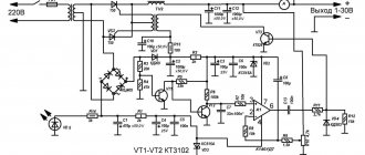
Schematic diagram
The schematic diagram of the SMPS is shown in the figure.
The architecture of this power supply is reminiscent of the SMPS of ATX format computers. The mains voltage is supplied through fuses FU1 and FU2 to the surge protector and standby power transformer. The use of two fuses is necessary for safety reasons - with one common fuse, in the event of a short circuit in the T1 winding, the current in its circuit will be insufficient to blow this fuse, and the power released by the failed transformer is sufficient to ignite it.
The surge filter contains a two-winding inductor L1, X-capacitors C1, C2 and Y-capacitors C3, C4 and has no special features. Varistor RV1 protects the SMPS from high-voltage surges in the network and when the network voltage exceeds the maximum permissible value.
NTC thermistor RK1 limits the charging current of capacitor C5 when the SMPS is connected to the network.
The voltage rectified by bridge VD1 and smoothed by capacitor C5 is supplied to a half-bridge inverter formed by MOS transistors VT1, VT2 and capacitor divider capacitors C6, C7. The separate construction of the input filter and capacitive divider makes it possible to facilitate the operation of the oxide filter capacitor, which has a relatively large ESR value. Resistors R5, R6 equalize the voltage on the divider capacitors.
The T4 power pulse transformer is included in the diagonal of the half-bridge.
The output circuits of the SMPS contain rectifiers using diodes VD5 - VD8, VD9 - VD12, a group stabilization choke (GS) L3 and U-shaped filters C11 - C16, L4, L5 and C17 - C22, L6, L7. Ceramic capacitors C13, C14, C17, C18 facilitate the operation of the corresponding electrolytes. Resistors R11 – R14 create the initial load necessary for normal operation of the SMPS at idle.
Chains C8, R7; C9, R9; C10, R10 – damping. They limit emissions of EMF, self-inductance, and leakage inductance and reduce the interference created by SMPS.
The control circuit did not fit on the main board, so it was assembled in the form of an A1 module on an additional board.
As you probably already guessed, its basis is the DA2 UC3825AN chip. It is powered by an integral stabilizer on the KRENK DA1. Capacitors C1 and C7 – power filter. They, as the DS says, should be located as close as possible to the corresponding DA2 pins. Capacitor C5 and resistor R8 are frequency-setting. With the ratings indicated in the diagram, the conversion frequency of the power supply is approximately equal to 56 kHz (the operating frequency of the IC is 2 times higher - after all, we have a push-pull SMPS). Capacitor C4 sets the duration of the soft start, in this case 78 ms. Capacitor C2 filters noise at the output of the reference voltage source. Elements C6, R9, R10 are the error amplifier compensation circuit, and R4, R6 are the output voltage divider of the power supply unit, from which the feedback signal is removed.
Overcurrent protection is implemented on current transformer T3. The signal from its secondary winding is rectified by a rectifier using diodes VD3, VD4 (main board). Resistor R8 (on the main board) is the current transformer load. The signal from R8 through the filter chain R7, C3 (in module A1) is supplied to the current limiting input DA2. This power supply unit implements clock-by-clock current limitation, i.e. the microcircuit does not allow the current through the switches to build up to dangerous values. When the voltage reaches 1 V at pin 9, the microcircuit limits the pulse width. If a short circuit occurs in the load and the switch current increases faster than DA2 has time to react to this, the voltage at pin 9 will exceed 1.4 V. The microcircuit discharges C4 and is switched off. The current in the primary winding circuit disappears and the microcircuit restarts. Thus, during a short circuit in the load, the SMPS goes into a “hiccupping” mode.
The gate control of field-effect transistors is implemented using transformer T2. Currently, the use of all sorts of bootstrap high-voltage drivers such as IR2110, etc. has become widespread. However, the disadvantage of such microcircuits is that if any element fails, the ENTIRE high-voltage part of the power supply and the galvanically connected nodes burn out (which is what I had to deal with encounter these microcircuits during experiments). In addition, these ICs do not provide galvanic isolation of the control circuit from the high-voltage part, which is unacceptable with the selected architecture. You can read about the features of gate control in [3], and in [4] you can download a program for calculating the control transformer.
Schottky diodes VD1 – VD4 in module A1 protect the driver outputs of the control chip. This is also facilitated by resistor R11.
The SMPS switch-off circuit is assembled on elements VT1, VT2, R1 – R5. The point of all this is to short-circuit C4, thereby putting the control chip into standby mode. Such bells and whistles are needed to ensure that the SMPS is turned off even if the shutdown input suddenly hangs in the air (the percentage in the control unit burns out, the wire breaks) or the standby power supply fails. In other words, the operation of DA2 will be blocked as long as power is supplied to it and the log level is not applied to the SMPS control input. 1.
The SMPS has a standby power supply that can be used to power the amplifier control unit with the remote switching function.
The basis of the standby power supply is transformer T1. The use of a “regular” 50-Hz transformer increases the reliability of the device compared to the pulsed flyback converters that are widely used in computer power supplies, which very often die, creating various pyrotechnic effects. After all, the duty room requires round-the-clock work. The voltage rectified by bridge VD2 and smoothed by capacitor C23 (about 15 V) is supplied to module A1 and to the Step-Down (step-down) pulse converter on the well-known MC34063 (Russian analogue of K1156EU5AR). You can read about this little thing in DS [5]. Someone will say, why such difficulties? What didn't you like about Krenka? The fact is that for normal operation the UC3825 requires a minimum of 12 V over the entire permissible range of network voltages. At the maximum voltage in the network (we must take everything into account), the output of the VD2 bridge can be as much as 18-20 V. Moreover, if your microprocessor unit consumes more than 50 mA, the Krenka will turn into a large stove.
The VD14 suppressor protects the duty load (your mega-complicated and super-sophisticated microcontroller control unit) in the event of a failure of the standby power supply (for example, if the MC34063 key fails, all 15 V may appear at its output).
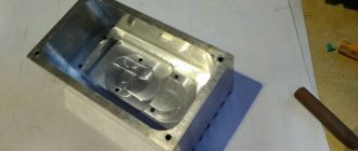
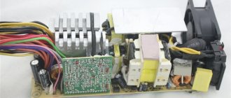
Construction and details
Since I don’t like “snot”, and this device loves correct wiring, the SMPS is assembled on a single-sided printed circuit board, the picture of which is given below: Two jumpers from MGTF wire are installed on the main board - J1 on the parts side and J2 on the track side. As noted above, the control circuit did not fit on the main board and is therefore assembled on an auxiliary board: The use of SMD elements here is caused not so much by the desire to make an ultra-small module and complicate the task of purchasing elements for radio amateurs from regions remote from Moscow, but by the requirements for wiring high-frequency circuits around the UC3825. Thanks to the use of SMD elements, it was possible to make all printed conductors of a minimum length. Anyone who wants can try to draw a beautiful scarf using ordinary details - I didn’t succeed =))
I will also note that I strongly do not recommend deviating too much from the given board layout, since the power supply may either start to “crap” on the air or will not work at all.
Now about the details. Many of them can be pulled out of faulty or outdated computer power supplies. The main board is designed to install resistors C2-23 (MLT, OMLT, etc.), resistors R10, R13 and R14 are imported (they are thinner than MLT). Ceramic capacitors - K10-17B or similar imported ones, C25 must be made of NPO dielectric or similar, C6, C7 - film K73-17.
Interference suppression capacitors C1, C2 must be of category X2, and C3 and C4 - Y2. For the latter, this requirement is mandatory, since the electrical safety of the SMPS depends on them. Capacitors C8 – C10 are imported high-voltage ceramic disk capacitors. You can install K15-5, but they are larger, you will have to adjust the board.
All oxide capacitors must be of Low Equivalent Series Resistance (Low ESR). Jamicon WL series capacitors are suitable. Jamicon HS is suitable for C5.
Throttle L1 is from a computer power supply, torn out from a similar place. Mine said “YX EE-25-02”. Chokes L2, L4, L5 are standard on dumbbells with a diameter of 9 mm, for example, the RLB0914 series. Choke L2 must be designed for a current of at least 0.8 A, L4, L5 - at least 0.5 A. Chokes L6 and L7 are wound on T72 rings (K18.3x7.11x6.60) from sprayed iron grade -26 (yellow- white). I used ready-made ones, so I don’t know how many turns there are, but if desired, the number of turns can be calculated in the “DrosselRing” program [6]. The measured inductance of my chokes is 287 µH.
Transistors VT1, VT2 are n-channel MOSFETs with a drain-source voltage of at least 500 V and a drain current of at least 8 A. You should select transistors with a minimum open channel resistance (Rds_on) and a minimum gate charge.
Bridge VD1 – any 800-1000 V, 6A, VD2 – any >50V, 1A. KD522 is suitable as VD3, VD4. Diodes VD5 - VD8 - Schottky for a voltage of at least 80 V and a current of at least 1 A, VD9 - VD12 - high-speed (ultrafast) for a voltage of at least 200 V, a current of 10...15 A and a reverse recovery time of no more than 35 ns (at most case 75...50 ns). It will be absolutely gorgeous if you find a Schottky for this voltage. Diode VD13 - any Schottky 40 V, 1A.
Module A1 uses SMD resistors and capacitors of size 0805. A jumper 0805 is installed at position J1. C5 must be made of an NPO dielectric or similar, C6 must be no worse than X7R. C1 – tantalum type C or D – pads on the board are designed for any of them. Transistors VT1, VT2 - any npn in a SOT23 package. Diodes VD1 - VD4 - any Schottky for a current of 3A in an SMC package. DA1 can be replaced with 7812.
XP3 – connector from ATX motherboard.
Transformer T1 type TP121-8, TP131-8. Any one with an output voltage under load of 15 V and a power of 4.5 VA will do. Winding data for other inductive elements is given below.
Control transformer T2
| Winding | Contact No. (N-K) | Number of turns | The wire |
| I | 4-2 | 16 | MGTF-0.08 |
| II | 10-9 | 16 | MGTF-0.08 |
| III | 6-7 | 16 | MGTF-0.08 |
| Magnetic core | Ferrite ring T90 (K22.9x14.0x9.53) green, u=4600 | ||
Each winding occupies 1 layer and is evenly distributed around the ring. First, winding I is wound and covered with a layer of insulation, for example, fluoroplastic tape or varnished cloth. The insulation on this winding determines the safety of the SMPS. Next, windings II and III are wound. The ring is glued vertically to a plastic socket with contacts, which is then soldered into the board. It should be noted that for normal operation this transformer must have a minimum leakage inductance, therefore the core for it must be toroidal and with maximum magnetic permeability. I tried to wind this trans on an E20/10/6 core from N67 - the pulses on the gates had emissions that slightly opened the second transistor of the half-bridge:
The blue graph is the pulses at the gate of VT2, the yellow graph is the voltage at the drain of VT2.
With a toroidal transformer wound as described above, the oscillogram looks like this: When installing the control transformer, it is necessary to observe the phasing of the windings! If the phasing is incorrect, the half-bridge transistors will burn out when turned on!
Current transformer T3
| Winding | Contact No. (N-K) | Number of turns | The wire |
| I | — | 1 | MGTF-0.35 |
| II | 1-2-3 | 2x75 | PEV-2 0.23 |
| Magnetic core | 2 rings K12x8x6 made of M3000NM ferrite | ||
Winding II is wound into 2 wires; after winding, the end of one half-winding is connected to the beginning of the other and contact 2. Winding I is a piece of wire passed through a ring in the shape of the letter “P”. To increase the electrical and mechanical strength of the insulation, a fluoroplastic tube is placed on the wire.
Power pulse transformer T4
| Winding | Contact No. (N-K) | Number of turns | The wire |
| I | 4 – 2 | 18+18 | 3xPEV-2 0.41 |
| II | 9 – 7 – 8 | 6+6 | PEV-2 0.41 |
| III | 10 – 11 – 12 | 9+9 | 5xPEV-2 0.41 |
| Magnetic core | EI 33.0/24.0/12.7/9.7 PC40 TDK ferrite | ||
The transformer is calculated using the ExcellentIT(5000) program [7]. The core is removed from the computer power supply. First, the first half of winding I is wound. An insulation layer is laid on top of it (I use lavsan film from photoresist) and a screen - an open turn of copper tape wrapped with tape. The screen is connected to terminal 2 of the transformer. Next, several layers of film or varnished fabric are placed and winding III is wound with a bundle of 10 wires. You need to wind it turn to turn, squeezing the bundle with your fingers so that all 10 wires are arranged in one row - otherwise it won’t fit. The end of one half-winding (5 wires) is connected to the beginning of the other and terminal 11 of the frame. Winding III is covered with one layer of lavsan film, on top of which winding II is laid similarly to III. After this, several more layers of film or varnished cloth are laid, an open turn of insulated copper foil connected to terminal 2, a layer of film, and the second half of the primary winding is wound.
This winding of the transformer makes it possible to reduce the leakage inductance by four times.
PTFE tubes are placed on all terminals of the primary winding.
Group stabilization throttle L3
| Winding | Number of turns | The wire | |
| L3.1 | 24 | PEV-2 0.457 | |
| L3.2 | 24 | PEV-2 0.457 | |
| L3.3 | 40 | PEV-2 0.8 | |
| L3.4 | 40 | PEV-2 0.8 | |
| Magnetic core | Ring T106 (K26.9x14.5x11.1) from sprayed iron -26 (yellow-white) | ||
GVD was calculated using the CalcGRI program [8].
First, windings L3.3 and L3.4 are wound simultaneously in 2 wires. They will take 2 layers. Windings L3.1 and L3.2 are similarly wound on top of them in one layer. When installing the DGS on the board, it is necessary to observe the phasing of the windings!
It is recommended to impregnate all winding products with PLASTIK-71 varnish.
Transistors VT1, VT2 are installed on an aluminum finned radiator with dimensions of 60x15x40 mm and a surface area of 124 cm2. Diodes VD9 – VD12 are installed on a similar radiator with dimensions of 83x15x40 mm and an area of 191 cm2. With the specified heat sink area, the power supply is capable of operating for a long time under a constant load of no more than 100 W! If the SMPS is intended to be used not for an amplifier, but to power a load with a constant power consumption of up to 200 W, the area of the radiators must be increased or forced cooling must be applied!
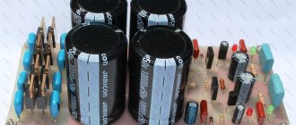
The assembled SMPS looks like this:
Assembly and configuration
First, all elements are installed on the board except VD1, VT1, VT2, T4, R7, C8, FU1. Connect the SMPS to the network and check for the presence of +5 V voltage on pin 11 of the XP3 connector. After this, connect pins 1 and 11 of connector XP3 and connect a two-beam oscilloscope in parallel with resistors R3 and R4 (oscillation ground to the lower ends of the resistors, signal probes to the upper ends. With transistors installed and power supplied, this cannot be done!!!). The oscillogram should look like this:
If suddenly your pulses turn out to be in phase, it means you made a mistake when unsoldering the windings of transformer T2. Swap the beginning and end of the lower or upper winding. If this is not done, then when you turn on the SMPS with the keys there will be a large and colorful fireworks display
If you do not have a dual-beam oscilloscope, you can check the shape and presence of pulses with a single-beam one at a time, but you can only rely on your own care when wiring the T4 transformer.
If you still haven’t exploded, haven’t gotten hot, the pulses are there and are phased correctly, you can solder in all the missing elements and turn it on for the first time. Just in case, I recommend doing this through a 150-watt Ilyich light bulb (if you can buy it :D). In a good way, in order not to burn anything, it must, of course, be included in the open circuit between plus C5 and the half-bridge. But since we have a printed circuit board, this is difficult to do. When plugged into a break in the network cable, it is of little use, but still somehow calmer)). We turn on the SMPS at idle and measure the output voltages. They should be approximately equal to nominal.
We connect a 100 W load between the “+25 V” and “-25 V” outputs. For these purposes, it is convenient to use a regular 220 V 2.2 kW kettle, having first filled it with water. One kettle loads the SMPS by approximately 90 - 100 W. We measure the output voltages again. If they differ significantly from the nominal values, we drive them within acceptable limits by selecting resistors R4 and R6 in module A1.
If the SMPS operates unstable - the output voltage fluctuates at a certain frequency, it is necessary to select feedback compensation elements C6, R9, R10. Increasing the capacitance of C10 increases the inertia of the SMPS and increases stability, however, an excessive increase in its capacitance will lead to a slowdown in the operating system and an increase in output voltage ripple. Now you can check the SMPS at maximum load. If the SMPS starts unstable under load or goes into a “hiccupping” mode, you can try to increase the capacitance of capacitor C3, but I don’t recommend getting too carried away with this - this will lead to a decrease in the speed of the current protection and an increase in shock overloads of the SMPS elements during a short circuit. You can also try reducing the R8 value. With the value indicated in the diagram, the protection is triggered when the current amplitude of the primary winding T4 is about 5 A. By the way, I will say that the maximum permissible drain current of the transistors used is 8 A.
If nothing has exploded, all transistors and capacitors remain in place, the power supply meets the characteristics given at the beginning of the article, and the kettle is warm, connect the amplifier to the power supply and enjoy the music while drinking freshly prepared tea
PS: I tested my SMPS together with an LM3886 amplifier. I didn’t notice any background in the speakers (which can’t be said about computer speakers with a “classic” transformer). I really liked the sound.
Happy building!
Literature
- Schemes of PWM controllers K1156EU2, K1156EU3 https://www.sitsemi.ru/kat/1156eu23.pdf
- Pulse width controllers of the KR1156EU2 and KR1156EU3 series. – Radio, 2003, No. 6, p. 47 – 50.
- Development and application of high-speed control circuits for power field-effect transistors https://valvolodin.narod.ru/articles/FETsCntr.pdf
- Calculation and application of GDT https://bsvi.ru/raschet-i-primenenie-gdt/
- DC-DC converter K1156EU5 https://www.sitsemi.ru/kat/1156eu5c.pdf
- Program "DrosselRing" https://radiokot.ru/forum/download/file.php?id=106660
- Program “ExcellentIT(5000)” https://radiokot.ru/forum/download/file.php?id=106659
- Program "CalcGRI" https://radiokot.ru/forum/download/file.php?id=106664
Files:
Board in Sprint Layout 5.0 format
All questions in the Forum.
| What do you think of this article? | Did this device work for you? | |
| 64 | 0 | 0 |
| 0 | 1 |
Description of circuit elements
Almost all elements can be found in an ATX power supply. Diodes D26-D29 with a breakdown voltage of 400 V, but it is better to take a little higher, at least 600 V. The finished rectifier can be found in the ATX power supply. It is also advisable to use diode bridges for powering the controller at least 600 V. But they can be cheap and popular 1N4007 or similar.
The zener diode that limits the controller supply voltage must withstand 0.7 W of power, so its power rating must be 1 W or more.
Capacitors C18 and C19 can be used with a different capacitance, but not less than 220 µF. Capacitances greater than 470 uF should also not be used due to the excessively increased current when the inverter is connected to the network and the large size - they may simply not fit on the board. Capacitors C18 and C19 are also found in each ATX power supply.
Power transistors Q8 and Q9 are very popular IRF840, available in most electronic stores for 30 rubles. In principle, you can use other 500V MOSFETs, but this will involve changing resistors R12 and R13. When set to 75 ohms, the gate open/close time is about 1 µs. Alternatively, they can be replaced with either 68 - 82 ohms.
Buffers in front of the MOSFET inputs and control transformer I, using BD135 / 136 transistors. Any other transistors with a breakdown voltage above 40 V can be used here, such as BC639 / BC640 or 2SC945 / 2SA1015. The latter can be torn out from ATX power supplies, monitors, etc. A very important element of the inverter is capacitor C10. This should be a polypropylene capacitor adapted to high pulse currents. This capacitor is found in ATX power supplies. Unfortunately, it is sometimes the cause of power supply failure, so you need to check it carefully before soldering it into the circuit.
The diodes D22-D25 that rectify +/- 35V are used UF5408 connected in parallel, but a better solution would be to use BY500/600 single diodes which have a lower drop voltage and higher current rating. If possible, these diodes should be soldered on long wires - this will improve their cooling.
Chokes L3 and L4 are wound on toroidal powder cores from ATX power supplies - they are characterized by a predominant yellow and white color. Cores with a diameter of 23 mm, 15-20 turns on each of them, are sufficient. However, tests have shown that they are not needed - the inverter works without them, reaches its power, but the transistors, diodes and capacitor C10 become hotter due to pulse currents. Reactors L3 and L4 improve inverter efficiency and reduce failure rates.
The D14-D17 +/- 12V rectifiers have a big impact on the efficiency of this line. If this line will power a preamp, additional fans, an additional headphone amplifier, and for example a level meter, diodes should be used at least 1 A. However, if the +/- 12 V line will only power the preamp, which pulls up to 80 mA , you can even use 1N4148 here. Chokes L1 and L2 are practically not needed, but their presence improves the filtering of interference from the power supply. As a last resort, you can use 4.7 Ohm resistors instead.
Voltage limiters R22 and R23 can consist of a series of power resistors connected in series or in parallel to produce a single higher power resistor and corresponding resistance.
Capacitors
A typical dependence of the impedance (impedance modulus) of an electrolytic capacitor with a capacity of 10,000 μF on frequency is shown in Figure 4 (according to the Nichicon company, I put the red dots on the graph). The dotted straight lines on the graph show the behavior of an ideal capacitor (line Xc) and an ideal inductor (line XL).
Rice. 4. Dependence of impedance (impedance modulus) of an electrolytic capacitor on frequency.
At low frequencies, the capacitor behaves “correctly”, and has the properties of a capacitor: as the frequency increases, its impedance decreases proportionally. This occurs to the left of point A in Figure 4 when the graph representing the properties of the capacitor coincides with the ideal line Xc. At higher frequencies (between points A and B), the capacitive properties of the capacitor deteriorate and its active resistance and inductance begin to affect. At point B, the capacitor is simply a resistor, but at higher frequencies (between points B and C) it is inductive. At even higher frequencies (to the right of point C), the capacitor is an inductance, where its properties coincide with the inductance line XL.
So the capacitor, whose characteristic is shown in Figure 4, works well at frequencies up to about 1 kHz, and at a frequency of 20 kHz it is practically a resistor. At higher frequencies it is an inductance. Capacitors with larger capacitances have an even lower maximum operating frequency.
In fact, not everything is as bad as it seems. Even at these high frequencies, the capacitor is able to store and release energy. That is, he works and does his job. But the fact that the capacitor exhibits the properties of inductance can cause unstable operation of the amplifier. Sometimes high-frequency oscillations occur in amplifiers (amplifiers self-excite) due to the inductive nature of the power supply circuit. Therefore, film capacitors of sufficiently large capacity are connected in parallel with electrolytic capacitors. They have a much higher maximum operating frequency and maintain capacitive operation in the audio and ultrasonic ranges, compensating for the inductive nature of electrolytic capacitors.
To be honest, film capacitors are not needed in this place. Inside the amplifier's power supply, which is made as a separate unit, additional film capacitors are practically of no use. Because the amplifier is connected to the power supply using a cable. The resistance and inductance of the cable “eat up” the entire capacitive component created by film capacitors. So the benefit of capacitors C13 and C14 is very small. But they don't do any harm. Such capacitors simply need to be installed on the amplifier board near the output transistors. In that place they work well, and without such capacitors installed on the amplifier board, it is almost impossible to obtain high sound quality. In the absence or insufficient capacity of these film capacitors on the amplifier board, high-frequency oscillations (oscillations) occur in the amplifiers. But since there is no harm from film capacitors, let them bring at least a little benefit. Ultimately, they will help suppress the high-frequency interference that passes through all our filters. With film capacitors, such interference has no chance. It is important that installing such capacitors on a printed circuit board does not worsen the performance of the power supply - so that the resistance and inductance of the conductors does not increase.
This amplifier power supply contains three pairs of electrolytic capacitors. How many pairs of capacitors should there be? When connected in parallel, the capacitances of the capacitors are summed up. Three 10,000 µF capacitors connected in parallel have an equivalent capacitance of 30,000 µF. Is it possible to use one capacitor with a capacity of 30,000 microfarads instead of these three capacitors? Can! Why didn't I do that? There are several reasons:
- high-capacity capacitors are scarce and expensive;
- high-capacity capacitors have large dimensions, so it is not always convenient to place them in the case;
- For the capacitor to operate most efficiently, its actual physical connection (the connection shown in the circuit diagram is fictitious) must be correct. Large capacitors are usually located outside the printed circuit board, and are connected by wires. In this case, it is more difficult to ensure correct connection, Fig. 5. And the resistance of the connecting wires will be greater.
Rice. 5. Correct connection of capacitors.
How many pairs of capacitors can you use? Usually from one to four or five. But most often it’s two or three. In this case, the design of the power supply is most convenient. By the way, using several capacitors of smaller capacity instead of one large one can be a good solution also because the smaller the capacitor’s capacity, the better its high-frequency properties (see Fig. 4).
Starting and setting up the inverter
After etching the boards, begin assembling the elements, starting from the smallest to the largest. It is necessary to solder all components except inductor L5. After completing assembly and checking the board, set the PR1 potentiometer to the leftmost position and connect the mains voltage to the 220 V INPUT connector. There should be a voltage of 18 V across the capacitor C1. If the voltage stops at approximately 14 V, this indicates a problem with the control of the transformer or power transistors, that is, a short circuit in the control circuit. Oscilloscope owners can check the voltage at the transistor gates. If the controller is working correctly, check that the MOSFET is switched correctly.
After turning on the 12 V power and the controller power supply, +/- 2 V should appear on the +/- 35 V line. This means that the transistors are controlled properly, one at a time. If the light on the 12V power supply was turned on and there was no voltage at the output, this would mean that both power transistors were opening at the same time. In this case, the control transformer must be disconnected, and the wires of one of the secondary windings of the transformer must be changed. Next, solder the transformer back and try again with a 12 V power supply and a lamp. If the test is successful and we get +/- 2 V at the output, you can turn off the lamp power supply and solder inductor L5. From this moment on, the inverter must operate from a 220 V network through a 60 W lamp. After connecting to the network, the light should blink briefly and immediately turn off completely. +/- 35 and +/- 12 V should appear at the output (or other voltage depending on the transformer speed ratio).
Load them with a small amount of power (for example, from an electronic load) for testing and the light at the input will start to glow a little. After this test, you need to switch the inverter directly to the network, and connect a load with a resistance of about 20 Ohms to the +/- 35 V line to check the power. PR1 should be adjusted so that the inverter does not turn off after charging the heater. When the inverter starts to heat up, you can check the voltage drop on the +/- 35V line and calculate the power output. A 5-10 minute test is sufficient to check the power output of the inverter. During this time, all components of the inverter will be able to heat up to their rated temperature. It is worth measuring the temperature of the MOSFET heatsink, it should not exceed 60C at an ambient temperature of 25C. Finally, you need to load the inverter with an amplifier and set the PR1 potentiometer as far to the left as possible, but so that the inverter does not turn off.
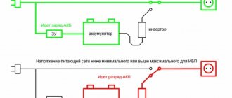
Separate meals?
Sometimes you can hear that a high-quality amplifier should have separate power supply - each of the stereo channels should be powered from a separate power supply. There is a “dual mono” amplifier design principle, when two independent mono amplifiers are installed in one housing. Sometimes amplifiers are even made in the form of monoblocks - a completely single-channel amplifier with its own power supply, placed in its own separate housing. In fact, the candy bar is a marketing gimmick. The dual-mono design reduces manufacturing costs: Instead of designing dual-channel circuit boards, the engineer is paid to design a single-channel circuit board that is half the size. Small single-channel boards are also cheaper to assemble and configure. And the defect of one small board causes less losses than a large two-channel board.
So is there a need for separate power supply for the stereo channels of the amplifier? I guess, yes. After all, power supply voltage drops caused by the operation of one amplifier channel fall into another channel. But let's figure out what's really going on. An experimental study of this issue is described in the article Separate power supply for stereo amplifier channels.
The mutual influence of amplifiers through a common power source occurs in two ways:
- Supply voltage sags caused by the operation of one amplifier channel lead to a decrease in supply voltage in the second channel. And therefore, to the possibility of clipping occurring in it.
- Power instability caused by another channel of the amplifier penetrates the “clean” channel of the amplifier and causes interference in it.
Let's start with the second point. The better the amplifier (this is built into its design), the less it is affected by interference coming from the power supply. There is even such an amplifier parameter: supply voltage ripple suppression (instability) ratio (PSRR, or kSVR).
For good amplifiers this coefficient is quite large. That is, with good amplifiers, interference coming from the power supply has virtually no effect on the amplified signal. Therefore, you don’t have to be afraid of them (if you do everything correctly). But with bad amplifiers with a low PSRR value, interference from the power supply circuit may well have a noticeable effect on the signal.
But then it turns out that separate power supply is more necessary for bad amplifiers!
Indeed, in high-quality amplifiers, noise in the power supply circuit is suppressed so well that the amount of it that enters the signal does not in any way affect the sound quality. The mutual interference of stereo channels along the power supply circuit is so small that it is lost against the background of other types of interference and distortion. Naturally, this only happens with proper design of the entire device as a whole. So we won’t get any problems from this side.
The first point is much more important - the effect of voltage sags caused by one channel on another channel of the amplifier. After all, if the supply voltage decreases, the maximum output power of the amplifier decreases. There is a possibility for clipping to occur. But in fact, one common power supply for several channels is no worse, and sometimes even better, than two separate units.
Let's conduct a thought experiment. Let's say we have a single-channel amplifier (or monoblock) designed to reproduce a monophonic signal. The amplifier is equipped with a power supply in which the transformer has a power of 50 W, and the capacity of the storage capacitors in the power filter is 10,000 μF. For a stereo signal you need to use two such amplifiers. We will combine them into a common housing and provide them with a common power supply. The resulting stereo version of the amplifier uses a transformer with a power of 100 W (=2∙50) and storage capacitors with a capacity of 20000 uF (=2∙10000). Now let's compare these two amplifiers: one with a dual mono structure, and the other a stereo with a "double" power supply.
Let's consider one of two extreme cases. Let's feed both stereo channels of this amplifier the same monophonic signal. It will make no difference whether the amplifier's two channels are powered by two separate power supplies or by one double power power supply. All voltages - maximum, minimum, average, as well as the amount of ripple will be the same. Because, on the one hand, we doubled the number of channels, and therefore the current consumption, and on the other hand, we also doubled the power of the power supply. So in this case there is no difference, one common power supply is used, or two separate ones.
Another extreme case. Now let's apply a stereo signal to the inputs of our amplifier. It differs from monophonic in that each channel has its own sound. So, the extreme case is that there is sound in one of the channels, but not in the other. This sometimes happens at the beginning or end of a musical composition. How do our stereo amplifiers behave, one of which is equipped with separate power supplies, and the second with a common power supply for two channels?
An amplifier with separate power supplies works like this: one of the channels is idle, and the second operates in standard mode. Its power is provided by storage capacitors with a capacity of 10,000 μF in its separate power supply. Accordingly, voltages and ripples have a given value.
An amplifier with a common power supply operates in improved conditions: it has the resources of both power channels at its disposal! That is, to obtain the same signal we use a 100 W transformer and storage capacitors with a capacity of 20,000 μF. As a result, the ripple will be half as much, and the minimum supply voltage will be slightly higher than that of an amplifier with separate power supplies.
Indeed, while one of the individual power supplies is idle, the common power supply operates at full capacity on the other amplifier channel.
The properties of a real stereo signal are approximately in the middle. The music volume is higher in one channel and then in the other. When the volume in one of the stereo channels is lower, the corresponding amplifier consumes less power from the power supply. And each time, the common power supply transfers the freed-up resources to the stereo channel that needs them more. This is equivalent to increasing the power supply power by approximately 5...15%. Separate power supplies are not capable of this.
I see this especially well when I use my AV receiver. It has five channels with a common power supply. When I listen to stereo audio, all the power from this power supply goes to the two front channel amplifiers. And these two amplifiers never lack power from the five-channel power supply.
Thus, there is no point in making separate power supplies for each of the amplifier channels.
But sometimes they still use separate power supplies. In these cases, there are always quite compelling reasons of a different nature. For example, one high-power transformer does not fit into the housing. Or two transformers are installed so that the magnetic fields they create cancel each other out. Or it is structurally more convenient to place two small power supplies in the case instead of one large one. Or each of the amplification channels should be a separate independent module with the ability to quickly increase the number of channels. Or something else.
Recommendations for installation and power increase
The inverter can be adapted to any power needs of various UMZCHs. When designing the plate, we tried to make it as universal as possible for mounting various types of elements. The location of the transformer and capacitors makes it possible to mount a fairly large heatsink for MOS transistors along the entire length of the board. After proper bending of the leads of the diode bridges, they can be installed in a metal case. Increasing the heat dissipation allows the converter power to be theoretically increased to 400 W. Then you need to use a transformer on the ETD39. This change requires 470uF capacitors C18 and C19, 1.5-2.2uF capacitors C10 and the use of 8 BY500 diodes.