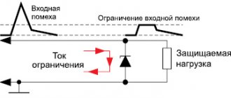
Designation and interpretation of diodes
Designation of the rectifier diode on the diagram according to GOST 2.730-73 ESKD. Conditional graphic designations in schemes. Semiconductor devices.” The appendix of this GOST shows the dimensions in a modular grid. It looks like this:
There are different options for designating diodes.
According to OST 11366.919-81 the following alphanumeric designation:
- 1) the first letter or number indicates the material:
- 1 (G)
- germanium Ge - 2 (K)
- silicon Si - 3 (A)
- gallium Ga - 4 (I)
- indium In - 2) The second letter is a subclass of a semiconductor device. For our case, this is the letter D.
- 3) The third number is the functionality of the element depending on the class (diodes, varicaps, zener diodes, etc.).
For example, for rectifier diodes (D):
101...199 - low power diodes with a constant or average forward current value of less than 0.3A.
201…299 - medium power diodes with a constant or average forward current value from 0.3 to 10A.
There are also high power diodes with a current of more than 10A. Heat removal for low power diodes is carried out through the housing, for medium and high power diodes through heat sinks.
Until 1982 there was a different classification:
- the first D - characterized the entire class of diodes
- Next came the digital code:
- from 1 to 100 - for point germanium diodes
- from 101 to 200 - for point silicon diodes
- from 201 to 300 - for planar silicon diodes
- from 301 to 400 - for planar germanium diodes
- from 401 to 500 - for mixing microwave detectors
- from 501 to 600 - for multiplying diodes
- from 601 to 700 - for video detectors
- from 701 to 749 - for parametric germanium diodes
- from 750 to 800 - for parametric silicon diodes
- from 801 to 900 - for zener diodes
- from 901 to 950 - for varicaps
- from 951 to 1000 - for tunnel diodes
- from 1001 to 1100 - for rectifying posts
JEDEC system (USA)
- the first digit is the number of pn junctions (1 - diode; 2 - transistor; 3 - thyristor)
- then N (type number) and serial number
- after that there may be a couple of numbers about the ratings and individual characteristics of the diode
Pro Electron System (Europe)
According to this system, devices are divided into industrial and household. Household devices are coded with two letters and three numbers from 100 to 999. Industrial devices will have three letters and two numbers from 10 to 99. For diodes:
- 1) first letter:
- A
- germanium Ge - B
- silicon Si - C
—gallium Ga - R
- other semiconductors
JIS System (Japan)
Used in countries of Asia and the Pacific region.
- the first digit is the number of transitions (0 - phototransistor, photodiode; 1 - diode; 2 - transistor; 3 - thyristor)
- then the letter S (semiconductors) - semiconductor
- then the letter corresponding to the type of device:
- A
- RF transistors pnp - B
- LF transistors pnp - C
- RF transistors npn - D
- low-frequency transistors npn - E
- diodes - F
- thyristors - G
- Gunn diodes - H
- unijunction transistors - J
- field effect transistors with p-channel - K
- field effect transistors with n-channel - M
- symmetrical thyristors - Q
- light emitting diodes - R
- rectifier diodes - S
- small signal diodes - T
- avalanche diodes - V
- varicaps, pin diodes, charge storage diodes - Z
- zener diodes, stabilizers, limiters - Reg. device number
- Device modification
- Next may be an index describing special properties
In our case there will be the letter R.
There are also special designations from manufacturers that differ from those given above.
Power classification
The power of the elements is determined by the maximum permissible direct current. In accordance with this characteristic, the following classification has been adopted:
- Low-current rectifier diodes, they are used in circuits with a current of no more than 0.3 A. The housing of such devices is usually made of plastic. Their distinctive features are light weight and small dimensions. Low power rectifier diodes
- Devices designed for average power can operate with current in the range of 0.3-10 A. Such elements, for the most part, are made of metal housing and equipped with rigid leads. On one of them, namely on the cathode, there is a thread that allows you to securely fix the diode on the radiator used for heat removal. Medium power rectifier diode
- Power semiconductor elements, they are designed for direct current over 10 A. Such devices are produced in metal-ceramic or metal-glass housings of the pin type (A in Fig. 4) or tablet type (B). Fig. 4. High power rectifier diodes
Operating principle of a rectifying diode
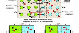
Semiconductors in their electrical properties are somewhere between conductors and dielectrics.
How does a diode behave when connected forward and reverse?
Forward direction
- the direction of direct current in which the diode has the least resistance.
Reverse direction
- the direction of direct current in which the diode has the greatest resistance.
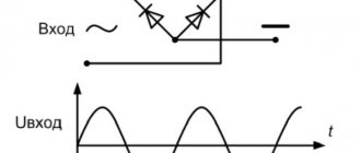
Let's consider the behavior of the current in the circuit during direct and reverse connection to alternating and direct voltage. Initially we will have a sine wave, which is obtained from an alternating current source.
With such connection methods, half of the sine wave, positive or negative, is cut off. The output is a pulsating alternating current of the same sign (consider it constant, the only catch is that no one uses it).
- anode
(for direct connection we connect to the positive), the base of the triangle - cathode
(connect to negative for direct connection) stick
The current flows from the anode to the cathode, some people compare it to a funnel. Liquid flows into a wide neck faster than into a narrow neck. The operating principle is to pass current when turned on directly and turn off the diode when turned on in reverse (no current). It's all about the blocking layer, which evaporates or expands depending on how the diode is connected.
Let's consider the behavior of a diode in a DC circuit. In the left image, current flows, voltage passes - the light is on (black) - this is a direct connection. In the right image, the diode is not passing enough current and voltage to light the bulb - reverse switching.
Diode device
The design of the first diodes has already been discussed. Diffusion devices were made by fusing a drop of n-conductivity material into a larger droplet of p-conductivity material, or vice versa. The “big drop” was often cooled by a heat sink in powerful devices. To protect the diode from damage, it was enclosed in a sealed, heat-dissipating metal housing with a glass insulator and a second electrode.
Planar diodes often have a completely different, more modern design. This is a thin flat crystal on a cooling substrate, subjected to complex photo- and chemical processing, and irradiated with ions from a doping gun. “Photo” is already outdated; they use not light, but hard UV rays or X-rays.
The principle is reminiscent of traditional photography: exposure and doping is done through templates, followed by etching (similar to photo development). Powerful diodes can be obtained by connecting several others in parallel. This makes the thermal load uniform across the substrate. In fact, this is the same technology used to produce microcircuits. Therefore, modern high-power diodes are made in thermoset plastic housings with metal heat sinks.
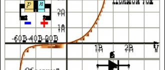
I-V characteristics of rectifier diodes (Ge, Si)
The current-voltage characteristics of diodes are graphs of forward and reverse currents (Y) and voltages (X) at different temperatures.
When a reverse voltage is applied that exceeds the threshold value, the reverse current increases and a breakdown of the pn layer occurs. It is worth paying attention to the orders of numbers along the axes. The magnitude of the reverse current is an order of magnitude smaller than the forward current. The forward voltage values are an order of magnitude lower than the reverse voltage. Upon reaching the threshold value of the forward voltage, the forward current begins to increase like an avalanche.
The difference between the diodes is that the reverse current of silicon diodes is less than that of germanium diodes. Therefore, due to the higher current, in Ge diodes the breakdown is thermal in nature, while in Si diodes the electrical breakdown predominates. The power dissipated at the same currents is less for germanium diodes.
Ohm's law in electrical engineering
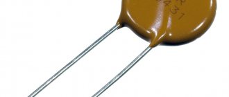
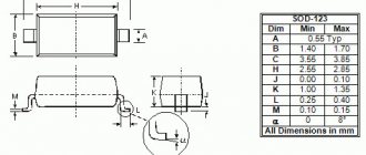
DataSheet
Diode housing KD203
Description
Silicon diodes, diffusion.
Designed to convert alternating voltage with a frequency of up to 5 kHz. Available in metal-glass housing with rigid leads. The type of diode and the connection diagram of the electrodes with the leads are shown on the case. The weight of the diode with its components is no more than 18 g. When mounted on a heat sink or chassis, the diode must be held by the hexagonal base with a key. The tightening force should not exceed 1.96 N m (0.2 kgf m). During installation, it is prohibited to apply a force exceeding 4.9 N (0.5 kgf) to the insulated terminal of the diode.
Series and parallel connection of diodes is allowed in the presence of shunt and additional resistors. The resistance of resistors is calculated using the formulas:
where n is the number of switched diodes;
e is the current utilization factor of diodes. When operating diodes on a capacitive load, the effective value of the current through the diode should not exceed 1.57 Ipp, avg, max. Parameters of the KD203 diode
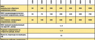
| Parameter | Designation | Marking | Meaning | Unit change |
| Maximum constant reverse voltage. | Uo6p max, Uo6p and max | KD203A | 420 | IN |
| KD203B | 560 | |||
| KD203V | 560 | |||
| KD203G | 1000 | |||
| KD203D | 720 | |||
| KD203E | 800 | |||
| KD203Zh | 800 | |||
| KD203I | 1000 | |||
| KD203K | 1000 | |||
| KD203L | 400 | |||
| KD203M | 600 | |||
| Maximum direct forward current. | Ipp max, Ipp avg max, I*pp and max | KD203A | 10 | A |
| KD203B | 10 | |||
| KD203V | 10 | |||
| KD203G | 10 | |||
| KD203D | 10 | |||
| KD203E | 10 | |||
| KD203Zh | 10 | |||
| KD203I | 10 | |||
| KD203K | 10 | |||
| KD203L | 10 | |||
| KD203M | 10 | |||
| Maximum diode operating frequency | fd max | KD203A | 1 | kHz |
| KD203B | 1 | |||
| KD203V | 1 | |||
| KD203G | 1 | |||
| KD203D | 1 | |||
| KD203E | 1 | |||
| KD203Zh | 1 | |||
| KD203I | 1 | |||
| KD203K | 1 | |||
| KD203L | 1 | |||
| KD203M | 1 | |||
| Constant forward voltage | Upr no more (at Ipr, mA) | KD203A | 1(10 A) | IN |
| KD203B | 1(10 A) | |||
| KD203V | 1(10 A) | |||
| KD203G | 1(10 A) | |||
| KD203D | 1(10 A) | |||
| KD203E | 1(5 A) | |||
| KD203Zh | 1(10 A) | |||
| KD203I | 1(5 A) | |||
| KD203K | 1(10 A) | |||
| KD203L | 1(10 A) | |||
| KD203M | 1(10 A) | |||
| Constant reverse current | Irev no more (at Urev, V) | KD203A | 1500 (600) | µA |
| KD203B | 1500 (800) | |||
| KD203V | 1500 (800) | |||
| KD203G | 1500 (1000) | |||
| KD203D | 1500 (1000) | |||
| KD203E | 1500 (800) | |||
| KD203Zh | 1500 (800) | |||
| KD203I | 1500 (1000) | |||
| KD203K | 1500 (1000) | |||
| KD203L | 1500 (400) | |||
| KD203M | 1500 (600) | |||
| Reverse recovery time - the time the diode switches from a given forward current to a given reverse voltage from the moment the current passes through the zero value until the reverse current reaches the specified value | tvos, arr | KD203A | — | mks |
| KD203B | — | |||
| KD203V | — | |||
| KD203G | — | |||
| KD203D | — | |||
| KD203E | — | |||
| KD203Zh | — | |||
| KD203I | — | |||
| KD203K | — | |||
| KD203L | — | |||
| KD203M | — | |||
| Total capacity | SD (at Uarb, V) | KD203A | — | pF |
| KD203B | — | |||
| KD203V | — | |||
| KD203G | — | |||
| KD203D | — | |||
| KD203E | — | |||
| KD203Zh | — | |||
| KD203I | — | |||
| KD203K | — | |||
| KD203L | — | |||
| KD203M | — |
For a description of values with asterisks (*), see the letter designations of the diode parameters.
If you find an error, please select a piece of text and press Ctrl+Enter.
Straightening principle
Any rectifying device has two terminals or electrodes, called anode and cathode. Each of them is connected to plates of the corresponding conductivity that form the semiconductor junction (the anode is with the “p” layer, and the cathode is with the “n” layer). At the moments when a plus is supplied to the anode of the diode, and a minus is supplied to its cathode (in the case of the so-called “direct” connection), the device passes current while in the open state.
If the polarity of the incoming voltage changes its sign (reverse switching on of the diode), according to its current-voltage characteristic, no current flows through the semiconductor junction. As a result of one-way conductivity of the device, a pulsating current signal is formed at its output (it is shown in the photo below).
Straightening effect
According to this circuit, after the diode VD, the rectified signal Un goes to the load R (without filtering for now), where it is used for its intended purpose.
Note! If an alternating voltage of a certain amplitude U is applied to the input of a rectifier device, the current through it and the load R will flow only in one direction.
As a result of rectification, a series of positive half-waves will appear at the load, which are subsequently supplied to electrolytic capacitors for the purpose of filtering. Only after smoothing out the ripples through capacitors will it be possible to talk about the finally rectified voltage.