How does a diode work?
You may not physically see the diodes themselves, but the result of their action surrounds us everywhere. These devices allow you to control the flow of current in a specified direction. There are many different versions of diodes. In what cases is this necessary? Below we will discuss examples and, to some extent, the operating principle of semiconductor diodes. If you add two metal plates to the P and N working areas of the material, you get anode and cathode electrodes. The scheme for connecting the electrodes to the source can work as follows: applying voltage from the battery to the N electrode ensures the attraction of positrons, respectively, to the P electrode – electrons; the absence of tension returns everything to its original state; changing the polarity of the applied voltage ensures the attraction of electrons in the opposite direction to the positive plate, and positrons to the negative one. In the latter case, excess charges accumulate on the metal plates, while a dead insulating zone is formed in the center of the material itself.
Large Signal Modeling
Shockley diode model
The Shockley Diode Equation relates the diode current I {displaystyle I} of the pn junction diode to the diode voltage VD {displaystyle V_{D}}. This connection is the I-V
:
I = I S ( e VD n V T − 1 ) {displaystyle I = I_ {S} left (e ^ {frac {V_ {D}} {nV_ {ext {T}}}} — 1ight)} ,
where I S {displaystyle I_{S}} is the saturation current
or
scale
diode current (the amount of current flowing at a negative VD {displaystyle V_ {D}} in excess of several V T {displaystyle V_ {ext {T}}} , usually 10−12 A). The scaling current is proportional to the cross-sectional area of the diode. Continuing the symbols: V T {displaystyle V_{ext {T}}} is the thermal voltage ( k T / q {displaystyle kT / q} , about 26 mV at normal temperature), and n {displaystyle n} is known as the diode ideality factor ( for silicon diodes n {displaystyle n} is approximately 1 to 2).
When VD ≫ n V T {displaystyle V_ {D} gg nV_ {ext {T}}} the formula can be simplified to:
I ≈ I S ⋅ e VD p V T {displaystyle Iapprox I_ {S} cdot e ^ {frac {V_ {D}} {nV_ {ext {T}}}}} .
However, this expression is only an approximation of a more complex current-voltage characteristic. Its applicability is particularly limited in the case of ultrafine contacts, for which more advanced analytical models exist.[2]
Example of a diode-resistor circuit
To illustrate the complexities of using this law, consider the diode voltage problem in Figure 1.
Figure 1: Diode circuit with resistive load.
Since the current flowing through the diode is the same as the current in the entire circuit, we can formulate another equation. K Kirchhoff's Laws, the current flowing in the circuit is equal to
i = VS − VD r {displaystyle I = {frac {V_ {S} -V_ {D}} {R}}} .
These two equations determine the diode current and diode voltage. To solve these two equations, we could replace the current I {displaystyle I} from the second equation into the first one, and then try rearranging the resulting equation to get VD {displaystyle V_{D}} in terms of VS {displaystyle V_{S}} . The complexity of this method is that the diode law is nonlinear. However, a formula expressing I {displaystyle I} directly in terms of VS {displaystyle V_{S}} without involving VD {displaystyle V_{D}} can be obtained using Lambert W
-function, which is the inverse function of f ( w ) = w e w {displaystyle f (w) = we ^ {w}} , that is, w = W ( f ) {displaystyle w = W (f)} . This solution is discussed below.
Explicit solution
An explicit expression for the diode current can be obtained through Lambert W
-function (also called Omega function).[3]
Below is a guide to these manipulations. The new variable w {displaystyle w} is entered as w = i S r p V T ( i i S + 1 ) {displaystyle w = {frac {I_ {S} R} {nV_ {ext {T}}}} left ({ frac {I} {I_{S}}} + 1ight)} .
After substitutions I / I S = e VD / n V T − 1 {displaystyle I / I_ {S} = e ^ {V_{D} / nV_ {ext {T}}} — 1} :
w e w = I S R p V T e VD p V T e i S r p V T ( I I S + 1 ) {displaystyle we ^ {w} = {frac {I_ {S} R} {nV_ {ext {T}}}} e ^ {frac {V_ {D}} {nV_ {ext {T}}}} e ^ { {frac {I_ {S} R} {nV_ {ext {T}}}} left ( {frac {I} {I_{S}}} + 1ight)}}
and VD = VS − i r {displaystyle V_{D} = V_{S} -IR} :
w e w = i S r p V T e VS p V T e − i r p V T e i r i S p V T i S e i S r p V T {displaystyle we ^ {w} = {frac { I_ {S} R} {nV_ {ext {T}}}} e ^ {frac {V_ {S}} {nV_ { ext {T}}}} e ^ { frac {-IR} {nV_ { ext {T }}}} e ^ {frac {IRI_ {S}} {nV_ {ext {T}} I_ {S}}} e ^ {frac {I_ {S} R} {nV_ { ext {T}}}}}
restructuring of the diode law from the point of view of w
becomes:
w e w = i S r p V T e V s + i s r p V T {displaystyle we ^ {w} = {frac {I_ {S} R} {nV_ {ext {T}}}} e ^{frac {V_{s} + I_{s}R}{nV_{ext {T} }}}} ,
which with the help of Lambert's W {displaystyle W} -function becomes
w = W ( i S r p V T e V s + i s r p V T ) {displaystyle w = Wleft ({frac {I_{S} R} {nV_ {ext {T}}}} e ^ {frac {V_ {s} + I_ {s} R} {nV_ { ext {T}}}) } ight)} .
With the approximations (relevant for the most common parameter values) I s R ≪ VS {displaystyle I_ {s} Rll V_ {S}} and I / I S ≫ 1 {displaystyle I / I_ {S} gg 1} , this solution becomes
i ≈ n V T r W ( i S r n V T e V s n V T ) {displaystyle Iapprox {frac {nV_ { ext {T}}} {R}} Wleft ({frac {I_ {S} R} {nV_{ext {T}}}} e ^ {frac {V_ {s}} { nV_ {ext {T}}}} ight)} .
Once the current is determined, the voltage across the diode can be found using any of the other equations.
For large x, W ( x ) {displaystyle W (x)} can be approximately estimated W ( x ) = ln x − ln ln x + o ( 1 ) {displaystyle W (x) = ln x-ln ln x + o (1)} . For general physical parameters and resistances I S r p V T e V s p V T {displaystyle {frac {I_{S} R} {nV_{ext {T}}}} e^{frac {V_{s}} { nV_ {ext {T}}}}} will be about 1040.
Iterative solution
The diode voltage VD {displaystyle V_{D}} can be found in terms of VS {displaystyle V_{S}} for any particular set of values by an iterative method using a calculator or computer.[4] The diode law is rearranged by dividing by I S {displaystyle I_ {S}} , and adding 1. The diode law becomes
e VD p V T = I I S + 1 {displaystyle e^{frac {V_ {D}} {nV_ {ext {T}}}}} = {frac {I} {I_ {S}}} + 1} .
Taking the natural logarithm of both sides, the exponent is removed and the equation becomes
VD p V T = ln ( I I S + 1 ) {displaystyle {frac {V_ {D}} {nV_ { ext {T}}}} = ln left ({frac {I} {I_ {S}}} + 1ight)} .
For any i {displaystyle I} , this equation determines VD {displaystyle V_{D}} . However, I{displaystyle I} must also satisfy the above Kirchhoff's law equation. This expression is replaced with I {displaystyle I} to get
VD p V T = ln ( VS − VD r i S + 1 ) {displaystyle {frac {V_ {D}} {nV_ { ext {T}}}} = ln left ({frac {V_ {S} -V_ {D}} {RI_ {S}}} + 1ight)} ,
or
VD = n V T ln ( VS − VD r i S + 1 ) {displaystyle V_ {D} = nV_ { ext {T}} ln left ({frac {V_ {S} -V_ {D}} {RI_ { S}}} + 1ight)} .
The source voltage VS {displaystyle V_{S}} is a known given value, but VD {displaystyle V_{D}} is on either side of the equation, requiring an iterative solution: the initial value for VD {displaystyle V_{D}} is guessed and placed in the right side of the equation. By performing various operations on the right side, we come up with a new value for VD {displaystyle V_{D}} . This new value is now substituted into the right-hand side, and so on. If this iteration converges
the values VD {displaystyle V_{D}} get closer and closer to each other as the process continues, and we can stop the iteration when the accuracy is sufficient. Once VD {displaystyle V_{D}} is found, I {displaystyle I} can be found from the equation of Kirchhoff's law.
Sometimes the iterative procedure depends critically on the first assumption. In this example, almost any first guess will do, for example VD = 600 mV {displaystyle V_{D} = 600, {ext {mV}}} . Sometimes the iteration procedure does not converge at all: in this problem, the iteration based on the exponential function does not converge, and so the equations were transformed to use the logarithm. Finding a convergent iterative formulation is an art, and every problem is different.
Graphic solution
Graphic determination of the operating point through the intersection of the diode characteristic with the resistive load line.
Graphical analysis is a simple way to obtain a numerical solution to the transcendental equations that describe a diode. Like most graphical methods, it has the advantage of simple visualization. Having built I
-
V
curves, you can obtain an approximate solution with any arbitrary degree of accuracy. This process is the graphical equivalent of the previous two approaches, which are more suitable for computer implementation.
This method plots two current-voltage equations on a graph, and the point where the two curves intersect satisfies both equations, giving the value of the current flowing through the circuit and the voltage across the diode. The figure illustrates this method.
Piecewise linear model
Piecewise linear approximation of the diode characteristic.
In practice, the graphical method is complex and impractical for complex circuits. Another diode modeling method is called piecewise linear
(PWL)
modeling
. In mathematics, this means breaking a function into several linear segments. This method is used to approximate the characteristic curve of a diode as a series of line segments. A real diode is modeled as 3 components connected in series: an ideal diode, a voltage source, and a resistor.
The figure shows the real I-V characteristic of the diode, approximated by a two-segment piecewise linear model. Typically, the slant line segment is selected tangent to the diode curve at the Q-point. Then the slope of this line is determined by the reciprocal of the small-signal resistance of the diode at point Q.
Mathematically idealized diode
CVC of an ideal diode.
First, consider a mathematically idealized diode. In such an ideal diode, if the diode is reverse biased, the current flowing through it is zero. This ideal diode starts conducting at 0V, and at any positive voltage, infinite current flows and the diode acts as a short circuit. The I-V characteristics of an ideal diode are shown below:
Ideal diode in series with voltage source
Now consider the case where we add a voltage source in series with the diode as shown below:
An ideal diode with a series voltage source.
When forward biased, an ideal diode is simply a short circuit, and when reverse biased, it is an open circuit.
If the anode of the diode is connected to 0 V, the voltage to the cathode will be in W
and therefore the potential at the cathode will be greater than the potential at the anode and the diode will be reverse biased.
In order for the diode to conduct, the voltage at the anode must be equal
to
W. This circuit approximately corresponds to the turn-on voltage of real diodes. The combined I-V characteristic of this circuit is shown below: I-V characteristic of an ideal diode with a series voltage source.
The Shockley diode model can be used to predict the approximate value of Vt {displaystyle V_{t}}.
i = i S ( e VD p ⋅ V T − 1 ) ⇔ ln ( 1 + i i S ) = VD p ⋅ V T ⇔ VD = p ⋅ V T ln ( 1 + i i S ) ≈ p ⋅ V T lane ( I I S ) ⇔ VD ≈ p ⋅ V T ⋅ lane 10 ⋅ log 10 ( I I S ) {displaystyle {egin {align} & I = I_ {S} left (e ^ {frac {V_ {D}} {ncdot V_ {ext {T}}}}} — 1ight) Leftrightarrow {} & ln left (1+ {frac {I} {I_ {S}}} ight) = {frac {V_ {D} } {ncdot V_ {ext {T}}}} Leftrightarrow {} & V_ {D} = ncdot V_ {ext {T}} ln left (1+ {frac {I} {I_ {S}}} ight) approximately ncdot V_ {ext {T}} ln left ({frac {I} {I_ {S}}} ight) Leftrightarrow {} & V_ { D} approximately ncdot V_ {ext {T}} cdot ln {10} cdot log _ { 10} {left ({frac {I} {I_{S}}} ight)} end {aligned}}}
Using n = 1 {displaystyle n = 1} and T = 25°C {displaystyle T = 25, {ext {°C}}} :
VD ≈ 0.05916 ⋅ log 10 ( I I S ) {displaystyle V_ {D} approximately 0.05916cdot log _ {10} {left ({frac {I} {I_ {S}}} ight)}}
Typical saturation current values at room temperature are:
- I S = 10 − 12 {displaystyle I_{S} = 10^{- 12}} for silicon diodes;
- I S = 10 − 6 {displaystyle I_ {S} = 10 ^ {- 6}} for germanium diodes.
As an option, VD {displaystyle V_{D}} comes with the logarithm of the ratio I I S {displaystyle {frac {I} {I_{S}}}} , its value changes very little with a large change in the ratio. Using base 10 logarithms makes it easier to think in orders of magnitude.
For 1.0 mA current:
- VD ≈ 0.53 V {displaystyle V_{D} approximately 0.53, {ext {V}}} for silicon diodes (9 orders of magnitude);
- VD ≈ 0.18 V {displaystyle V_{D} approximately 0.18, {ext {V}}} for germanium diodes (3 orders).
For 100 mA current:
- VD ≈ 0.65 V {displaystyle V_{D} approximately 0.65, {ext {V}}} for silicon diodes (11 orders);
- VD ≈ 0.30 V {displaystyle V_{D} approximately 0.30, {ext {V}}} for germanium diodes (5 orders of magnitude).
For silicon diodes, 0.6 or 0.7 volts are commonly used.[5]
Diode with voltage source and current limiting resistor
The last thing needed is a current limiting resistor, as shown below:
An ideal diode with a series voltage source and a resistor.
B IV
The characteristics of the final circuit look like this:
I-V characteristics of an ideal diode with a series voltage source and a resistor.
The real diode can now be replaced by a combination ideal diode, voltage source, and resistor, and the circuit can then be simulated using only linear elements. If the slant segment touches the real diode curve at the Q-point, this example circuit has the same small-signal circuit at the Q-point as the real diode.
Dual PWL diodes or 3-Line PWL model
I-V curves of the standard PWL model (marked with red triangles) as described above. For reference, a standard Shockley diode model is shown (marked with blue diamonds). Shockley parameters: i
s = 1e - 12 A,
V
t = 0.0258 V
When greater accuracy is required when simulating the turn-on characteristic of a diode, the model can be improved by doubling the standard PWL model. This model uses two piecewise linear diodes connected in parallel to more accurately simulate a single diode.
PWL Diode model with 2 branches.
The upper branch has lower forward voltage and higher resistance. This allows the diode to turn on more smoothly and in this regard more closely simulates a real diode. The lower leg has a higher forward voltage and lower resistance, which produces high current at high voltage. I-V plot of this model (marked with red triangles) compared to the standard model with a Shockley diode (marked with blue diamonds). Shockley parameters: i
s = 1e - 12 A,
V
t = 0.0258 V
Diodes from foreign manufacturers
Schottky diode
A similar principle with some differences is used in the marking system for imported diodes. There are three standards:
- JEDEC - American. Each diode is represented by a set of designations in the form 1NXY, where X is the serial number and Y is the modification. All devices have the first two symbols, so they are not taken into account in the color marking. Each number or letter has its own color, according to the table.
- PRO-ELECTRON – European. The two letters at the beginning are the material and subcategory of the diode. The serial number can take the form of a value from 100 to 999 (household appliances) or with the addition of letters (Z10-A99), implying industrial use. Each of the values is encoded into a color element.
- JIS - Japanese. It is noticeably different from the previous ones - the functional type is indicated at the beginning: photodiode, conventional diode, transistor or thyristor. Then comes S - the designation of the semiconductor; the next letter is the type of device within the category, then the serial number and modification letter (one or two).
Color marking according to foreign systems
It is almost impossible to remember all the combinations. If you understand at least the basic correspondences, you will be able to understand the purpose of the diode much faster.
Read also: Everything about the types of monitor matrix
How to determine the parameters of an LED by appearance?
The easiest way is to find out the characteristics of an LED by its appearance. To do this, just type the following phrase into the search engine: “buy LED.” Next, from the list provided, you should select the largest online store and find the corresponding section of the catalog. Then carefully review all available positions and if luck smiles on you, you will find what you are looking for. As a rule, in serious online stores where radio-electronic elements are sold, each item has the corresponding documentation, datasheet or basic characteristics. By comparing the appearance of the existing LED with the one in the catalog, you can thus find out its characteristics.
The following approach is used by more experienced electronics engineers. However, there is nothing complicated about it. The vast majority of LEDs are divided into indicator and general purpose. Indicator lamps, as a rule, shine less brightly than others. This is understandable, because very bright light is not needed for indication. Indicator LEDs are used to signal the operation of various electronic devices. For example, when plugged into a power outlet, they indicate that the device is energized. They are found in kettles, laptops, switches, chargers, computers, etc. Their electrical parameters, regardless of appearance, are as follows: current – 20 mA = 0.02 A; voltage averages 2 V (from 1.8 V to 2.3 V).
General purpose LEDs shine brighter than the previous ones, so they can be used as lighting devices. However, they will also work for display if the current is reduced. Oddly enough, the vast majority of such LEDs also have a rated current consumption of 20 mA. But their voltage can range from 1.8 to 3.6 V. Super-bright LEDs are also in this class. At the same current, their voltage is usually higher - 3.0...3.6 V.
In general, LEDs of this type have a standard size range, the main parameter of which is the diameter of the lens circle or the width and thickness of the side if the lens is rectangular in shape.
Lens diameter, mm: 3; 4.8; 5; 8 and 10.
Reverse voltage
Reverse voltage is a type of energy signal created when the polarity of an electrical current is reversed. This voltage often occurs when reverse polarity is applied to a diode, causing the diode to react by operating in the opposite direction. This reverse function can also create a breakdown voltage within the diode, as this often breaks the circuit to which the voltage is applied.
Reverse voltage occurs when the power signal connection source to a circuit is applied in an inverted manner. This means that the positive lead source is connected to the ground or negative conductor of the circuit and vice versa. This voltage transfer is often not intended, as most electrical circuits are not capable of handling voltages.
When minimum voltage is applied to a circuit or diode, it may cause the circuit or diode to operate in reverse. This may cause a reaction such as the box fan motor turning incorrectly. The element will continue to function in such cases.
When the amount of voltage applied to a circuit is too large, the signal for the receiving circuit, however, is called breakdown voltage. If the input signal that has been reversed exceeds the allowable voltage for the circuit to maintain, the circuit may be damaged beyond the rest of the usable. The point at which the circuit is damaged refers to the breakdown voltage value. This breakdown voltage has a couple of other names, reverse peak voltage or reverse breakdown voltage.
Reverse voltage can cause breakdown voltage, which also affects the operation of other circuit components. Beyond the damaging diodes and reverse voltage circuit functions, it can also become a reverse voltage peak. In such cases, the circuit cannot contain the amount of input power from the signal that has been reversed, and may create a breakdown voltage between the insulators.
This breakdown voltage, which can occur across circuit components, can cause breakdown of components or wire insulators. This can turn them into signal conductors and damage the circuit by conducting voltage to different parts of the circuit that should not receive it, causing instability throughout the circuit. This can cause voltage arcs from component to component, which can also be powerful enough to ignite various circuit components and cause a fire.
LED markings
There are fewer difficulties in identifying LEDs. Each type has characteristic external distinctive features. There are two categories:
- SMD LED color. In turn, they are divided into groups according to radiation: multi-color diodes, neutral, warm and cold white.
- Element size. By analogy with foreign coding, 4 digits are used, which indicate the size in millimeters. 3014 – size 3 x 1.4 mm.
The number in front of the LED type means the quantity per 1 meter of strip. For devices with long leads enclosed in a plastic or glass case, a system of color elements is used, which can be found in the table.
Example of LED color coding
What does a diode consist of?
In our world there are substances that perfectly conduct electric current. This mainly includes metals, for example, silver, copper, aluminum, gold and so on. Such substances are called conductors. There are substances that conduct electricity very poorly - porcelain, plastics, glass, and so on. They are called dielectrics or insulators. Between conductors and dielectrics are semiconductors . These are mainly germanium and silicon.
Once germanium or silicon is mixed with a minute fraction of arsenic or indium, an N-type semiconductor is formed when mixed with arsenic; or a P-type semiconductor when mixed with indium.
Now if these two P and N type semiconductors are welded together, a PN junction is formed at their junction. This is the structure of a diode. That is, the diode consists of a PN junction.
diode structure
The P-type semiconductor in the diode is the anode, and the N-type semiconductor is the cathode.
Let's open the Soviet D226 diode and see what's inside it by grinding off part of the body on an emery wheel.
diode D226
This is the same PN junction
PN junction diode
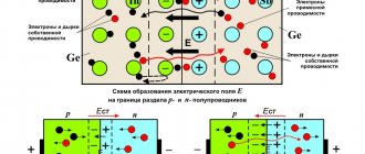
Direct diode connection
The pn junction of the diode can be affected by voltage supplied from external sources. Indicators such as magnitude and polarity will affect its behavior and the electrical current conducted through it.
Below we consider in detail the option in which the positive pole is connected to the p-type region, and the negative pole to the n-type region. In this case, direct switching will occur:
- Under the influence of voltage
from an external source, an electric field will be formed in the pn junction, and its direction will be opposite to the internal diffusion field. - The field voltage
will decrease significantly, which will cause a sharp narrowing of the blocking layer. - Under the influence of these processes,
a significant number of electrons will be able to freely move from the p-region to the n-region, as well as in the opposite direction. - The drift current indicators
during this process remain the same, since they directly depend only on the number of minority charged carriers located in the pn junction region. - Electrons
have an increased level of diffusion, which leads to the injection of minority carriers. In other words, in the n-region there will be an increase in the number of holes, and in the p-region an increased concentration of electrons will be recorded. - The lack of equilibrium and an increased number of minority carriers
causes them to go deep into the semiconductor and mix with its structure, which ultimately leads to the destruction of its electrical neutrality properties.
In this case, the semiconductor
Marking
In order to determine the type and find out the characteristics of a semiconductor diode, manufacturers apply special designations to the element body. It consists of four parts.
In the first place is a letter or number indicating the material from which the diode is made. Can take the following values:
- G (1) - germanium;
- K (2) - silicon;
- A (3) - gallium arsenide;
- And (4) - indium.
On the second - diode types. They can also have different meanings:
- D - rectifier;
- B - varicap;
- A - ultra-high frequency;
- I - tunnel;
- C - zener diodes;
- C - rectifying posts and blocks.
In third place is a number indicating the area of application of the element.
The fourth place is numbers from 01 to 99, indicating the serial number of the development.
Additional markings may also be applied to the body. But, as a rule, they are used in specialized devices and circuits.
For ease of perception, diodes can also be marked with various graphic symbols, for example, dots and stripes. There is no particular logic in such drawings. That is, to determine what kind of diode it is, you will have to look at a special correspondence table.
Old notation system
In accordance with the notation system developed before 1964, the abbreviated designation for diodes consisted of two or three elements .
The first element is letter, D - diode.
The second element is a number corresponding to the type of diode: 1...100 - point germanium, 101...200 - point silicon, 201...300 - planar silicon, 801...900 - zener diodes, 901...950 - varicaps, 1001...1100 - rectifier columns. The third element is a letter indicating the type of device. This element may be missing if there are no diode varieties.
Currently, there is a notation system corresponding to GOST 10862-72. In the new, as in the old system, the following division into groups according to the maximum (limiting) frequency of amplification (current transmission) is accepted into:
- low-frequency LF (up to 3 MHz),
- midrange frequency (from 3 to 30 MHz),
- high frequency HF (over 30 MHz),
- ultra-high frequency microwaves;
By power dissipation:
- low-power (up to 0.3 W),
- average power (from 0.3 to 1.5 W),
- high (over 1.5 W) power.
Marking of imported diodes
Currently, foreign-made SMD diodes are widely used. The design of the elements is made in the form of a board, on the surface of which a chip is fixed. The dimensions of the product are too small to allow marking to be applied to it. On larger elements, designations are present in full or abbreviated versions.
In electronics, SMD diodes make up about 80% of all products of this type used. Such a variety of details makes you pay more attention to the designations. Sometimes they may not coincide with the declared technical characteristics, so it is advisable to carry out additional checks of questionable elements if they are planned for use in complex and precise circuits. It should be borne in mind that the markings of diodes of this type may be different on completely identical cases. Sometimes there are only alphabetic symbols, without any numbers. In this regard, it is recommended to use tables with diode sizes from different manufacturers.
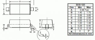
For SMD diodes, the SOD123 package type is most often used. A colored stripe or embossing may be applied to one of the ends, which indicates a cathode with negative polarity to open the pn junction. The only inscription corresponds to the designation of the case.
The type of housing does not play a decisive role when using a diode. One of the main characteristics is the dissipation of some amount of heat from the surface of the element. In addition, the values of the operating and reverse voltages, the maximum permissible current through the pn junction, power dissipation and other parameters are taken into account. All this data is indicated in reference books, and marking only speeds up the search for the desired element.
It is not always possible to determine the manufacturer by the appearance of the case. To find the desired product, there are special search engines into which you need to enter numbers and letters in a certain sequence. In some cases, diode assemblies do not carry any information at all, so in such cases only a reference book can help. Such simplifications, which make the diode designation very short, are explained by the extremely limited space for marking. When using screen or laser printing, it is possible to fit 8 characters per 4 mm2.
It is also worth considering the fact that the same alphanumeric code can denote completely different elements. In such cases, the entire electrical circuit is analyzed.
Reverse voltage
Reverse voltage is a type of energy signal created when the polarity of an electrical current is reversed. This voltage often occurs when reverse polarity is applied to a diode, causing the diode to react by operating in the opposite direction. This reverse function can also create a breakdown voltage within the diode, as this often breaks the circuit to which the voltage is applied.
Reverse voltage occurs when the power signal connection source to a circuit is applied in an inverted manner. This means that the positive lead source is connected to the ground or negative conductor of the circuit and vice versa. This voltage transfer is often not intended, as most electrical circuits are not capable of handling voltages.
When minimum voltage is applied to a circuit or diode, it may cause the circuit or diode to operate in reverse. This may cause a reaction such as the box fan motor turning incorrectly. The element will continue to function in such cases.
When the amount of voltage applied to a circuit is too large, the signal for the receiving circuit, however, is called breakdown voltage. If the input signal that has been reversed exceeds the allowable voltage for the circuit to maintain, the circuit may be damaged beyond the rest of the usable. The point at which the circuit is damaged refers to the breakdown voltage value. This breakdown voltage has a couple of other names, reverse peak voltage or reverse breakdown voltage.
Reverse voltage can cause breakdown voltage, which also affects the operation of other circuit components. Beyond the damaging diodes and reverse voltage circuit functions, it can also become a reverse voltage peak. In such cases, the circuit cannot contain the amount of input power from the signal that has been reversed, and may create a breakdown voltage between the insulators.
This breakdown voltage, which can occur across circuit components, can cause breakdown of components or wire insulators. This can turn them into signal conductors and damage the circuit by conducting voltage to different parts of the circuit that should not receive it, causing instability throughout the circuit. This can cause voltage arcs from component to component, which can also be powerful enough to ignite various circuit components and cause a fire.
Nuances
In addition to such diode designations, some graphical indicators are also used. Thanks to them, you can solve the problem and understand how high the operating point of the device is. Sometimes the diodes are marked with information about what production technique was chosen, what housing material is available, and the weight of the device. In principle, such information will be useful to those who create equipment; amateurs do not need such data.
It should be noted that imported manufacturers work according to a different scheme. The marking of a diode of this type will be quite simple; its meaning can be found in a special table. That is why analogues will be very easy to find.
Types of diodes by junction size
Based on the size and nature of the pn junction, three types of devices are distinguished - planar, point and microalloy.
Planar parts
represent one semiconductor wafer in which there are two regions with different impurity conductivity. The most popular products are made of germanium and silicon. The advantages of such models are the ability to operate at significant direct currents and in conditions of high humidity. Due to their high barrier capacitance, they can only operate at low frequencies. Their main applications are AC rectifiers installed in power supplies. These models are called rectifiers.
Point diodes
have an extremely small pn junction area and are adapted to work with low currents. They are called high-frequency because they are used mainly to convert modulated oscillations of significant frequency.
Microalloy
models are obtained by fusing single crystals of p-type and n-type semiconductors. According to the principle of operation, such devices are planar, but their characteristics are similar to point devices.
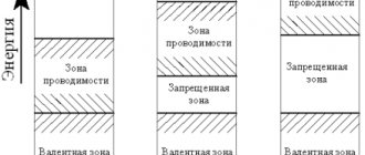
Diode operation and its current-voltage characteristics
The current-voltage characteristic of these devices is understood as a curved line that shows the dependence of the electric current flowing through the pn junction on the volume and polarity of the voltage acting on it.
Such a graph can be described as follows:
- The axis is located vertically: the upper area corresponds to the forward current values, the lower area to the reverse current parameters.
- Horizontal axis: The area on the right is for forward voltage values; area on the left for reverse voltage parameters.
- The direct branch of the current-voltage characteristic reflects the passing electric current through the diode. It is directed upward and runs in close proximity to the vertical axis, since it represents the increase in forward electric current that occurs when the corresponding voltage increases.
- The second (reverse) branch corresponds to and displays the state of the closed electric current, which also passes through the device. Its position is such that it runs virtually parallel to the horizontal axis. The steeper this branch approaches the vertical, the higher the rectifying capabilities of a particular diode.
- According to the graph, it can be observed that after an increase in the forward voltage flowing through the pn junction, a slow increase in the electric current occurs. However, gradually, the curve reaches an area in which a jump is noticeable, after which an accelerated increase in its indicators occurs. This is due to the diode opening and conducting current at forward voltage. For devices made of germanium, this occurs at a voltage of 0.1V to 0.2V (maximum value 1V), and for silicon elements a higher value is required from 0.5V to 0.6V (maximum value 1.5V).
- The indicated increase in current readings can lead to overheating of semiconductor molecules. If the heat removal that occurs due to natural processes and the operation of radiators is less than the level of its release, then the structure of the molecules can be destroyed, and this process will be irreversible. For this reason, it is necessary to limit the forward current parameters to prevent overheating of the semiconductor material. To do this, special resistors are added to the circuit, connected in series with the diodes.
- By examining the reverse branch, you can notice that if the reverse voltage applied to the pn junction begins to increase, then the increase in current parameters is virtually unnoticeable. However, in cases where the voltage reaches parameters exceeding the permissible norms, a sudden jump in the reverse current may occur, which will overheat the semiconductor and contribute to the subsequent breakdown of the pn junction.
SMD diodes
Marking SMD resistors
A feature of SMD diodes mounted directly on the surface of boards is the impossibility of full marking due to their small size. Hence the unique identification system. Several ways to distinguish such diodes:
- Pay attention to the shape of the housing. Each type has a characteristic appearance, for example, electrolytic capacitors are cylindrical, ceramic capacitors are parallelepiped-shaped.
- Check the size chart. Usually these are four digits that indicate the dimensions of the resistor in inches.
Each type of case and purpose has its own designation system, which makes decoding inconvenient.
SMD diodes - markings differ depending on the housing
SMD diode polarity
The small size also does not allow for the usual visible polarity markings. When determining the cathode, the following is used:
- markings in the form of colored rings are applied to its side;
- some cases without color symbols have a groove on the cathode side;
- if a triangle is depicted on the case, its apex points to the negative pole.
This helps avoid confusion. Most often, in all marking systems, symbols are applied to the cathode side, this is also true for SMD elements.
Small Signal Simulation
Resistance
Using Shockley's equation, the resistance of a small-signal diode R D {displaystyle r_ {D}} diode can be obtained about some operating point (Q-point) where the DC bias current I Q {displaystyle I_{Q}} and the applied Q-point voltage is VQ { displaystyle V_{Q)) .[6] To begin with, the diode is a small-signal conduction
gram D {displaystyle g_{D}} is, that is, the change in current in the diode caused by a small change in voltage across the diode, divided by that change in voltage, namely:
gram D = d i d V |
Q = i s p ⋅ V T e VQ p ⋅ V T ≈ i Q p ⋅ V T {displaystyle g_{D} = left. {frac {dI} {dV}} ight | _ {Q} = {frac {I_{s}} {ncdot V_ {ext {T}}}} e ^ {frac {V_ {Q}} {ncdot V_ {ext {T}}}} approximately {frac {I_ {Q}} {ncdot V_ {ext {T}}}}} . The latter approximation assumes that the bias current IQ{displaystyle I_{Q}} is large enough so that the factor 1 in the parentheses of the Shockley diode equation can be ignored. This approximation is accurate even at fairly low voltages, since the thermal voltage V T ≈ 25 mV {displaystyle V_ { ext {T}} is about 25, { ext {mV}}} at 300 K, so VQ / V T {displaystyle V_ { Q}/V_{ext{T}}} tends to be large, which means the exponent is very large.
Noting that the small-signal resistance r D {displaystyle r_{D}} is the reciprocal of the small-signal conductance just found, the diode resistance is independent of AC but is dependent on DC and is given by
r D = p ⋅ V T i Q {displaystyle r_ {D} = {frac {ncdot V_ {ext {T}}} {I_ {Q}}}} .
Capacity
Charge in a diode carrying current I Q {displaystyle I_{Q}} as is known
Q = I Q τ F + QJ {displaystyle Q = I_{Q} au _{F} + Q_{J}} ,
where τ F {displaystyle au _ {F}} time of direct passage of charge carriers: [6] The first charge term is the charge passing through the diode when the current I Q {displaystyle I_ {Q}} flows. The second term is the charge accumulated in the connection itself, when it is treated as a simple capacitor; that is, in the form of a pair of electrodes with opposite charges on them. This is the charge accumulated on the diode due to the presence of voltage across it, regardless of how much current it conducts.
Likewise, as before, diode capacitance represents the change in diode charge as a function of diode voltage:
CD = d Q d VQ = d i Q d VQ τ F + d QJ d VQ ≈ i QV T τ F + CJ {displaystyle C_ {D} = {frac {dQ} {dV_ {Q}}} = {frac { dI_ {Q}} {dV_ {Q}}} au _ {F} + {frac {dQ_ {J}} { dV_ {Q}}} approximately {frac {I_ {Q}} {V_ { ext {T}} }} au_{F} + C_{J}} ,
where CJ = d QJ d VQ {displaystyle C_ {J} = {frac {dQ_ {J}} {dV_ {Q}}}} is the junction capacitance and the first term is called diffusion capacitance because it is related to the current diffusing through transition.
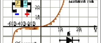
Diode Characteristics
Let's look at the characteristics of the KD411AM diode. We look for its characteristics on the Internet, typing into the search “datasheet KD411AM”
To explain the parameters of the diode, we also need its current-voltage characteristic
1) Reverse maximum voltage Urev is the voltage of the diode that it can withstand when connected in the reverse direction, while current Irev will flow through it - the current strength when the diode is connected in reverse. When the reverse voltage in the diode is exceeded, a so-called avalanche breakdown occurs, as a result of which the current sharply increases, which can lead to complete thermal destruction of the diode. In our diode under study, this voltage is 700 Volts.
2) Maximum forward current Ipr is the maximum current that can flow through the diode in the forward direction. In our case it is 2 Amperes.
3) Maximum frequency Fd , which must not be exceeded. In our case, the maximum diode frequency will be 30 kHz. If the frequency is higher, our diode will not work correctly.
Diodes. Main properties and characteristics
Semiconductor diode
called a semiconductor device with one
p
-
n
junction and two external leads from areas with conductivities of different types (anode A and cathode K).
According to their purpose, semiconductor diodes are divided into the following main types: rectifiers, zener diodes (reference diodes), fast recovery diodes (frequency diodes), photo- and LEDs, varicaps.
In addition to the indicated types of diodes, there are pulse, tunnel, magnetodiodes, strain gauge diodes, etc.
.
Most often, diodes are made of germanium (maximum permissible junction temperature Tj m =
80°C) and silicon
(Tj m =
180°C).
According to the design and technological principle, semiconductor diodes are divided into point and planar
.
A point diode uses a germanium or silicon plate with n
-type conductivity with a thickness of 0.1...0.6 mm and an area of 0.5...1.5 mm2.
A metal or alloy needle containing the necessary impurities is fused into the plate. During the fusing process, a p
-type layer is formed in the area of contact of the semiconductor with the needle.
In a planar diode p-n
- the junction is formed by two semiconductor layers of different types of conductivity, while the junction area for diodes of various types ranges from fractions of a square micrometer to several square centimeters.
Conventionally, semiconductor diodes are divided into low-current
(current limit less than 10 A) and
power
(current limit more than 10 A).
The conventional graphic designation of a semiconductor diode and its current-voltage characteristic are shown in Fig. 6.1.
The current-voltage characteristics of diodes are measured in a stationary mode, which does not allow their use in the analysis and calculation of electrical circuits containing diodes when exposed to high-frequency and pulsed signals. For these purposes, the so-called special small-signal equivalent circuit of a semiconductor diode is used, which includes the parameters pn
-transition without taking into account parasitic parameters of external terminals.
The main parameters of semiconductor diodes include parameters for voltage, current, resistance and power losses, switching phenomena, as well as temperature and thermal parameters.
The most important of them are:
- pulsed forward voltage UFM;
- threshold voltage U(TO);
- limit (average forward) current 1FAV;
- repeating pulse reverse current Irrm;
- differential forward resistance rT;
- reverse recovery time trr;
- pn
junction
temperature Tj
.
Rice. 6.1. Symbol and current-voltage characteristic of a semiconductor diode
Rice. 6.2. Straight-line approximation of the diode current-voltage characteristic
Threshold voltage U(TO)
determines the value of the forward voltage corresponding to the point of intersection of the line of rectilinear approximation of the straight line current-voltage characteristic with the stress axis (Fig. 6.2).
The maximum permissible average forward (limiting) current determines the maximum permissible average value of the forward current flowing through the diode for a long time over a period.
Differential forward resistance rT
determined by the angle of inclination of the line of rectilinear approximation of the direct current-voltage characteristic of the diode to the voltage axis (Fig. 6.2).
One type of planar semiconductor diode is a zener diode,
on the reverse branch of the current-voltage characteristic there is a section with a weak dependence of voltage on the magnitude of the reverse current.
As noted earlier, when the reverse voltage exceeds the breakdown voltage, an electrical breakdown p-n
-transition in which the reverse current increases sharply with an almost constant reverse voltage.
This phenomenon is used in zener diodes , used, for example, in parametric voltage stabilizers.
In Fig. 6.3, a
in the third quadrant of the current-voltage characteristic the reverse connection of the zener diode is shown. If the reverse current through the zener diode does not exceed the Istmax value, then the electrical breakdown does not lead to destruction of the junction and can be reproduced for an almost unlimited time (hundreds of thousands of hours).
Zener diodes are made on the basis of silicon, which is due to the need to obtain small values of Ist min
Zener diodes are characterized by the following main parameters:
1. Stabilization voltage U
st, i.e. the magnitude of the voltage on the zener diode when a given (rated) stabilization current flows through it, for example, Istnom (Fig. 6.3,
a).
In addition to the ICTnom value, the minimum Istmin and maximum Istmax values of currents in the stabilization section are also indicated, at which the specified reliability is ensured. The ICT min value is limited by the nonlinear portion of the I-V characteristic of the zener diode, and the ICTmax value is limited by the permissible dissipation power of the junction, after exceeding which its thermal breakdown occurs.
2. Differential resistance of the zener diode at the operating point in the stabilization section r
st =
dU
st
/ d
Ist in a given frequency range;
rst
characterizes the degree of change in the stabilization voltage when the current through the zener diode changes.
3. Temperature coefficient voltage stabilization
st =( dU
st /
dT
)100%, showing the magnitude of the relative change in stabilization voltage when the ambient temperature changes by 1 °C and is expressed as a percentage (Fig. 6.3,
b).
The level of stabilization voltage depends on the magnitude of the breakdown voltage UBR,
determined by the width of
the p-n
junction, i.e., the impurity concentration. For the manufacture of low-voltage zener diodes, in which the stabilization section is determined by the reverse current of a tunnel nature, highly doped silicon is used.
Due to the different nature of the breakdown of high-voltage and low-voltage zener diodes, the sign of st for them will also be different (Fig. 6.3, b).
For high-voltage zener diodes, st > 0, and for low-voltage zener diodes, the stabilization voltage decreases with increasing temperature and st < 0.
Voltage stabilization in the range of 0.3...1.0 V can be achieved by using the direct branch of the current-voltage characteristic, which for some silicon diodes is almost parallel to the current axis. Such diodes are called stabistors.
The industry also produces
two-anode zener diodes
that have a symmetrical current-voltage characteristic relative to the origin of coordinates. In this case, the stabilization voltages at positive and negative transition biases are the same.
To increase the stabilization voltage, zener diodes are connected in series, while parallel connection of zener diodes is unacceptable, since in this case the current will flow only through one zener diode, which has the lowest stabilization voltage.
Rice. 7.8. Volt-ampere characteristics of the zener diode (a)
and the dependence of -
(>
CT on the stabilization voltage
(b)
A varicap is a semiconductor diode used as a nonlinear capacitive element: It uses a barrier capacitance pn
-reverse-biased junction, caused by a change in charge in the junction when the applied voltage changes. Varicaps are made of silicon and are used in remote control and automatic frequency control systems.
^ The main parameters of the varicap are:
- capacity C,
fixed at a small reverse voltage (C = 10...500 pF);
— capacity overlap coefficient Kc=
Cmax/Cmin, characterizing the change in capacitance of the varicap in the operating range of voltage changes
(Ks=5...
20).
A tunnel diode is a semiconductor diode in which a tunnel effect occurs at low reverse and small forward voltages, and the forward branch of its current-voltage characteristic has a section with negative resistance (the so-called N-shaped characteristic). The tunnel effect consists of the leakage of electric charges (electrons and holes) through a potential barrier and is caused by the wave properties of microparticles. Tunnel diodes are made from germanium or gallium arsenide, which have very low resistance. Tunnel diodes are distinguished by their small size and weight, significant nonlinearity of the current-voltage characteristic, high speed, and the ability to operate in a wide temperature range (up to +600° C for gallium apsenide devices). Tunnel diodes are used in microwave generators with frequencies up to 10 GHz and amplifiers of electrical signals operating in a wide frequency and temperature range.
69. Bipolar transistors. Basic properties and characteristics.
General provisions. Transistor
called a semiconductor amplifier device with two
p-n
junctions and three external terminals. Currently, there is a large range of transistors that differ in power, maximum switching and generation frequencies, and other parameters.
All modern transistors are divided into two types: bipolar
and
field.
Bipolar transistors differ from field-effect transistors in their higher power level and higher operating frequency. At the same time, field-effect transistors are superior to bipolar transistors in terms of automatic gain control capabilities and can operate over a wider dynamic range.
When manufacturing transistors of various types, the same design and technological principles are used. ^ By technology
Manufacturing distinguishes between
alloy, diffusion and planar
transistors. Some types of transistors are made by combining several technologies (planar epitaxial) or manufacturing methods (mesaplanar, mesaplanar epitaxial). In the production of discrete transistors, planar-epitaxial technology is mainly used; in the production of transistors for integrated circuits, mesaplanar-epitaxial technology is used. Germanium and silicon are used to make transistors.
^ Bipolar transistors. The term " bipolar"
" means the presence of two types of charge carriers in the transistor: electrons and holes.
Depending on the type of conductivity of the outer layers, transistors are distinguished between n-p-p-types
(Fig. 6.4,
a and b
) and
p-n-p-types
(Fig. 6.4,
c and d
).
Rice. 6.4. Structure and graphic designation of transistors: a
and
b - p-p-
l-type;
c
and
d - p-p-p-tiia
The internal region of the transistor single crystal separating pn
-transitions P1 and P2 are called base (B).
The outer layer of the single crystal, which injects carriers into the base, is called the emitter (E), and the p-n
junction P1 adjacent to it is called the emitter. The second outer layer, which picks up carriers from the base, is called the collector (K), and the junction P2 adjacent to it is called collector. The base is the electrode that controls the amount of current through the transistor, since by changing the voltage between the emitter and the base, you can control the amount of injected (emitter), and therefore collector current.
If transition P1, under the influence of voltage UEB, is biased in the forward direction, and transition P2, under the influence of voltage UKB, is biased in the reverse direction, then this switching on of the transistor is called normal. When the polarity of the voltages UEB and UCB changes, the transistor turns on inversely.
Let's consider the principle of operation of the p-p-p
-type using the example of one of the possible schemes for its inclusion (Fig. 6.5).
In the absence of external voltages (UEB = UKB = 0), electric fields р-n
-transitions are created only by space charges of stationary ions and the established potential barriers of both transitions maintain dynamic equilibrium in the device, the currents in the transitions of which are equal to zero. In this case, the electric field in the base is also zero.
When connecting external voltage sources Ee
and
Ek
there is a redistribution of the electrical potentials of the transitions. When the transistor is turned on normally, conditions are created for the injection of holes from the emitter into the base and the movement of electrons from the base to the emitter. Since the base is the most high-resistivity region of a single crystal, the flow of electrons is significantly less than the counter flow of holes. Therefore, with the counter-movement of holes and electrons, their partial recombination occurs, and an excess of holes is introduced into the base layer, forming an emitter current Ie.
As a result of the injection of holes into the base, in which they are minority carriers, a hole concentration gradient arises in the latter, which leads to their diffusion movement in all directions, including the P2 transition. Minority carrier drift plays a minor role. When minority carriers move through the base, their concentration decreases due to recombination with electrons entering the base circuit from the source Ee.
The flow of these electrons forms the base current IB.
The period of time during which the concentration of minority carriers in the base decreases in e
times is called the minority carrier lifetime. Since the base thickness of modern transistors is a few micrometers, the time it takes for minority carriers to move through the base is significantly less than their lifetime.
Rice. 6.5. Circuit diagram for connecting a p-n-p-type transistor.
The transfer of current from the emitter circuit to the collector circuit is characterized by the current transfer coefficient of a bipolar transistor in a circuit with a common base:
Therefore, most of the holes reach the P2 transition and are captured by its field; the holes then recombine with electrons supplied by the power source Ek.
In this case, current Ik flows in the collector circuit. For transistor currents the following relation is true:
From the above relations it follows that
With modern transistors
Transistors p-p-p
-types work similarly, but when they are used, the polarity of the voltages of external sources is reversed.
A transistor with three external terminals is a four-terminal network. In this case, two terminals of the transistor form the input and output terminals, and the third is a common terminal for the input and output circuits. Depending on which electrode of the transistor is common to the input and output circuits of the quadripole, there are three connection schemes
transistor:
- with a common base (OB),
- common emitter (CE) and
- common collector (OK).
The most widely used circuit is the one with a common emitter.
To calculate circuits with bipolar transistors, families of static characteristics of transistors are used, which determine the relationship between the currents flowing through its external terminals and the voltages applied to these terminals.
These characteristics are usually:
- input at ;
- weekend at ;
- current transmission characteristics at
The SOB circuit does not amplify the current, but does amplify the voltage. It also has the property of amplifying the power of the input signal.
In a circuit with OE, the current transfer coefficient (base current transfer coefficient)
When changing in the range from 0.95 to 0.99, the value changes in the range from 20 to 100. Thus, the OE circuit has the property of significant current amplification. Since this circuit also has the property of voltage amplification, the power amplification in this circuit is much greater than in the circuit with OB.
Current transfer coefficient in a circuit with OK
Therefore, the circuit with OK has better current amplification than the circuit with OE, and, in addition, has the property of power amplification.
The characteristics of transistors are highly dependent on temperature. As the temperature rises, due to a significant increase in the number of minority charge carriers in the base and collector, the initial collector current sharply increases.
To prevent overheating of the collector p— p
-transition it is necessary that its power does not exceed the permissible value, i.e.
In Fig. Figure 6.6 shows, as an example, the output characteristics of a bipolar transistor connected according to a circuit with an OE. One of the limitations of the transistor output characteristic curves is the limitation on the permissible power value. To increase the permissible power of the transistor, its semiconductor structure is installed on a metal base, which is mounted on a special radiator.
If the voltage between the collector and emitter exceeds the permissible value, then electrical breakdown p
-I-transition. Therefore, there is a limitation on the output characteristics based on the collector voltage, i.e. . In addition, there is a limitation on the collector current due to the permissible heating of the emitter junction, i.e.
The area enclosed within the limiting lines is called the working area of the transistor characteristics.
To significantly increase the current transfer coefficient, a combination of two transistors connected according to the so-called Darlington circuit is used, which allows, for example, to increase the base current transfer coefficient to 300,000.
Rice. 6.6. Output characteristics of a bipolar transistor in a circuit with an OE and their limitations
Bipolar transistors are used in amplifiers, electrical signal generators, as well as in logic and pulse devices.
Semiconductor diode
called a semiconductor device with one
p
-
n
junction and two external leads from areas with conductivities of different types (anode A and cathode K).
According to their purpose, semiconductor diodes are divided into the following main types: rectifiers, zener diodes (reference diodes), fast recovery diodes (frequency diodes), photo- and LEDs, varicaps.
In addition to the indicated types of diodes, there are pulse, tunnel, magnetodiodes, strain gauge diodes, etc.
.
Most often, diodes are made of germanium (maximum permissible junction temperature Tj m =
80°C) and silicon
(Tj m =
180°C).
According to the design and technological principle, semiconductor diodes are divided into point and planar
.
A point diode uses a germanium or silicon plate with n
-type conductivity with a thickness of 0.1...0.6 mm and an area of 0.5...1.5 mm2.
A metal or alloy needle containing the necessary impurities is fused into the plate. During the fusing process, a p
-type layer is formed in the area of contact of the semiconductor with the needle.
In a planar diode p-n
- the junction is formed by two semiconductor layers of different types of conductivity, while the junction area for diodes of various types ranges from fractions of a square micrometer to several square centimeters.
Conventionally, semiconductor diodes are divided into low-current
(current limit less than 10 A) and
power
(current limit more than 10 A).
The conventional graphic designation of a semiconductor diode and its current-voltage characteristic are shown in Fig. 6.1.
The current-voltage characteristics of diodes are measured in a stationary mode, which does not allow their use in the analysis and calculation of electrical circuits containing diodes when exposed to high-frequency and pulsed signals. For these purposes, the so-called special small-signal equivalent circuit of a semiconductor diode is used, which includes the parameters pn
-transition without taking into account parasitic parameters of external terminals.
The main parameters of semiconductor diodes include parameters for voltage, current, resistance and power losses, switching phenomena, as well as temperature and thermal parameters.
The most important of them are:
- pulsed forward voltage UFM;
- threshold voltage U(TO);
- limit (average forward) current 1FAV;
- repeating pulse reverse current Irrm;
- differential forward resistance rT;
- reverse recovery time trr;
- pn
junction
temperature Tj
.
Rice. 6.1. Symbol and current-voltage characteristic of a semiconductor diode
Rice. 6.2. Straight-line approximation of the diode current-voltage characteristic
Threshold voltage U(TO)
determines the value of the forward voltage corresponding to the point of intersection of the line of rectilinear approximation of the straight line current-voltage characteristic with the stress axis (Fig. 6.2).
The maximum permissible average forward (limiting) current determines the maximum permissible average value of the forward current flowing through the diode for a long time over a period.
Differential forward resistance rT
determined by the angle of inclination of the line of rectilinear approximation of the direct current-voltage characteristic of the diode to the voltage axis (Fig. 6.2).
One type of planar semiconductor diode is a zener diode,
on the reverse branch of the current-voltage characteristic there is a section with a weak dependence of voltage on the magnitude of the reverse current.
As noted earlier, when the reverse voltage exceeds the breakdown voltage, an electrical breakdown p-n
-transition in which the reverse current increases sharply with an almost constant reverse voltage.
This phenomenon is used in zener diodes , used, for example, in parametric voltage stabilizers.
In Fig. 6.3, a
in the third quadrant of the current-voltage characteristic the reverse connection of the zener diode is shown. If the reverse current through the zener diode does not exceed the Istmax value, then the electrical breakdown does not lead to destruction of the junction and can be reproduced for an almost unlimited time (hundreds of thousands of hours).
Zener diodes are made on the basis of silicon, which is due to the need to obtain small values of Ist min
Zener diodes are characterized by the following main parameters:
1. Stabilization voltage U
st, i.e. the magnitude of the voltage on the zener diode when a given (rated) stabilization current flows through it, for example, Istnom (Fig. 6.3,
a).
In addition to the ICTnom value, the minimum Istmin and maximum Istmax values of currents in the stabilization section are also indicated, at which the specified reliability is ensured. The ICT min value is limited by the nonlinear portion of the I-V characteristic of the zener diode, and the ICTmax value is limited by the permissible dissipation power of the junction, after exceeding which its thermal breakdown occurs.
2. Differential resistance of the zener diode at the operating point in the stabilization section r
st =
dU
st
/ d
Ist in a given frequency range;
rst
characterizes the degree of change in the stabilization voltage when the current through the zener diode changes.
3. Temperature coefficient of voltage stabilization st =( dU
st /
dT
)100%, showing the magnitude of the relative change in stabilization voltage when the ambient temperature changes by 1 °C and is expressed as a percentage (Fig. 6.3,
b).
The level of stabilization voltage depends on the magnitude of the breakdown voltage UBR,
determined by the width of
the p-n
junction, i.e., the impurity concentration. For the manufacture of low-voltage zener diodes, in which the stabilization section is determined by the reverse current of a tunnel nature, highly doped silicon is used.
Due to the different nature of the breakdown of high-voltage and low-voltage zener diodes, the sign of st for them will also be different (Fig. 6.3, b).
For high-voltage zener diodes, st > 0, and for low-voltage zener diodes, the stabilization voltage decreases with increasing temperature and st < 0.
Voltage stabilization in the range of 0.3...1.0 V can be achieved by using the direct branch of the current-voltage characteristic, which for some silicon diodes is almost parallel to the current axis. Such diodes are called stabistors.
The industry also produces
two-anode zener diodes
that have a symmetrical current-voltage characteristic relative to the origin of coordinates. In this case, the stabilization voltages at positive and negative transition biases are the same.
To increase the stabilization voltage, zener diodes are connected in series, while parallel connection of zener diodes is unacceptable, since in this case the current will flow only through one zener diode, which has the lowest stabilization voltage.
Rice. 7.8. Volt-ampere characteristics of the zener diode (a)
and the dependence of -
(>
CT on the stabilization voltage
(b)
A varicap is a semiconductor diode used as a nonlinear capacitive element: It uses a barrier capacitance pn
-reverse-biased junction, caused by a change in charge in the junction when the applied voltage changes. Varicaps are made of silicon and are used in remote control and automatic frequency control systems.
^ The main parameters of the varicap are:
- capacity C,
fixed at a small reverse voltage (C = 10...500 pF);
— capacity overlap coefficient Kc=
Cmax/Cmin, characterizing the change in capacitance of the varicap in the operating range of voltage changes
(Ks=5...
20).
A tunnel diode is a semiconductor diode in which a tunnel effect occurs at low reverse and small forward voltages, and the forward branch of its current-voltage characteristic has a section with negative resistance (the so-called N-shaped characteristic). The tunnel effect consists of the leakage of electric charges (electrons and holes) through a potential barrier and is caused by the wave properties of microparticles. Tunnel diodes are made from germanium or gallium arsenide, which have very low resistance. Tunnel diodes are distinguished by their small size and weight, significant nonlinearity of the current-voltage characteristic, high speed, and the ability to operate in a wide temperature range (up to +600° C for gallium apsenide devices). Tunnel diodes are used in microwave generators with frequencies up to 10 GHz and amplifiers of electrical signals operating in a wide frequency and temperature range.
69. Bipolar transistors. Basic properties and characteristics.
General provisions. Transistor
called a semiconductor amplifier device with two
p-n
junctions and three external terminals. Currently, there is a large range of transistors that differ in power, maximum switching and generation frequencies, and other parameters.
All modern transistors are divided into two types: bipolar
and
field.
Bipolar transistors differ from field-effect transistors in their higher power level and higher operating frequency. At the same time, field-effect transistors are superior to bipolar transistors in terms of automatic gain control capabilities and can operate over a wider dynamic range.
When manufacturing transistors of various types, the same design and technological principles are used. ^ By technology
Manufacturing distinguishes between
alloy, diffusion and planar
transistors. Some types of transistors are made by combining several technologies (planar epitaxial) or manufacturing methods (mesaplanar, mesaplanar epitaxial). In the production of discrete transistors, planar-epitaxial technology is mainly used; in the production of transistors for integrated circuits, mesaplanar-epitaxial technology is used. Germanium and silicon are used to make transistors.
^ Bipolar transistors. The term " bipolar"
" means the presence of two types of charge carriers in the transistor: electrons and holes.
Depending on the type of conductivity of the outer layers, transistors are distinguished between n-p-p-types
(Fig. 6.4,
a and b
) and
p-n-p-types
(Fig. 6.4,
c and d
).
Rice. 6.4. Structure and graphic designation of transistors: a
and
b - p-p-
l-type;
c
and
d - p-p-p-tiia
The internal region of the transistor single crystal separating pn
-transitions P1 and P2 are called base (B).
The outer layer of the single crystal, which injects carriers into the base, is called the emitter (E), and the p-n
junction P1 adjacent to it is called the emitter. The second outer layer, which picks up carriers from the base, is called the collector (K), and the junction P2 adjacent to it is called collector. The base is the electrode that controls the amount of current through the transistor, since by changing the voltage between the emitter and the base, you can control the amount of injected (emitter), and therefore collector current.
If transition P1, under the influence of voltage UEB, is biased in the forward direction, and transition P2, under the influence of voltage UKB, is biased in the reverse direction, then this switching on of the transistor is called normal. When the polarity of the voltages UEB and UCB changes, the transistor turns on inversely.
Let's consider the principle of operation of the p-p-p
-type using the example of one of the possible schemes for its inclusion (Fig. 6.5).
In the absence of external voltages (UEB = UKB = 0), electric fields р-n
-transitions are created only by space charges of stationary ions and the established potential barriers of both transitions maintain dynamic equilibrium in the device, the currents in the transitions of which are equal to zero. In this case, the electric field in the base is also zero.
When connecting external voltage sources Ee
and
Ek
there is a redistribution of the electrical potentials of the transitions. When the transistor is turned on normally, conditions are created for the injection of holes from the emitter into the base and the movement of electrons from the base to the emitter. Since the base is the most high-resistivity region of a single crystal, the flow of electrons is significantly less than the counter flow of holes. Therefore, with the counter-movement of holes and electrons, their partial recombination occurs, and an excess of holes is introduced into the base layer, forming an emitter current Ie.
As a result of the injection of holes into the base, in which they are minority carriers, a hole concentration gradient arises in the latter, which leads to their diffusion movement in all directions, including the P2 transition. Minority carrier drift plays a minor role. When minority carriers move through the base, their concentration decreases due to recombination with electrons entering the base circuit from the source Ee.
The flow of these electrons forms the base current IB.
The period of time during which the concentration of minority carriers in the base decreases in e
times is called the minority carrier lifetime. Since the base thickness of modern transistors is a few micrometers, the time it takes for minority carriers to move through the base is significantly less than their lifetime.
Rice. 6.5. Circuit diagram for connecting a p-n-p-type transistor.
The transfer of current from the emitter circuit to the collector circuit is characterized by the current transfer coefficient of a bipolar transistor in a circuit with a common base:
Therefore, most of the holes reach the P2 transition and are captured by its field; the holes then recombine with electrons supplied by the power source Ek.
In this case, current Ik flows in the collector circuit. For transistor currents the following relation is true:
From the above relations it follows that
With modern transistors
Transistors p-p-p
-types work similarly, but when they are used, the polarity of the voltages of external sources is reversed.
A transistor with three external terminals is a four-terminal network. In this case, two terminals of the transistor form the input and output terminals, and the third is a common terminal for the input and output circuits. Depending on which electrode of the transistor is common to the input and output circuits of the quadripole, there are three connection schemes
transistor:
- with a common base (OB),
- common emitter (CE) and
- common collector (OK).
The most widely used circuit is the one with a common emitter.
To calculate circuits with bipolar transistors, families of static characteristics of transistors are used, which determine the relationship between the currents flowing through its external terminals and the voltages applied to these terminals.
These characteristics are usually:
- input at ;
- weekend at ;
- current transmission characteristics at
The SOB circuit does not amplify the current, but does amplify the voltage. It also has the property of amplifying the power of the input signal.
In a circuit with OE, the current transfer coefficient (base current transfer coefficient)
When changing in the range from 0.95 to 0.99, the value changes in the range from 20 to 100. Thus, the OE circuit has the property of significant current amplification. Since this circuit also has the property of voltage amplification, the power amplification in this circuit is much greater than in the circuit with OB.
Current transfer coefficient in a circuit with OK
Therefore, the circuit with OK has better current amplification than the circuit with OE, and, in addition, has the property of power amplification.
The characteristics of transistors are highly dependent on temperature. As the temperature rises, due to a significant increase in the number of minority charge carriers in the base and collector, the initial collector current sharply increases.
To prevent overheating of the collector p— p
-transition it is necessary that its power does not exceed the permissible value, i.e.
In Fig. Figure 6.6 shows, as an example, the output characteristics of a bipolar transistor connected according to a circuit with an OE. One of the limitations of the transistor output characteristic curves is the limitation on the permissible power value. To increase the permissible power of the transistor, its semiconductor structure is installed on a metal base, which is mounted on a special radiator.
If the voltage between the collector and emitter exceeds the permissible value, then electrical breakdown p
-I-transition. Therefore, there is a limitation on the output characteristics based on the collector voltage, i.e. . In addition, there is a limitation on the collector current due to the permissible heating of the emitter junction, i.e.
The area enclosed within the limiting lines is called the working area of the transistor characteristics.
To significantly increase the current transfer coefficient, a combination of two transistors connected according to the so-called Darlington circuit is used, which allows, for example, to increase the base current transfer coefficient to 300,000.
Rice. 6.6. Output characteristics of a bipolar transistor in a circuit with an OE and their limitations
Bipolar transistors are used in amplifiers, electrical signal generators, as well as in logic and pulse devices.