Transistors are designed to solve problems of amplifying and switching electrical signals. The time of rapid development of transistors was 50–80 years of the last century. Nowadays, it should be recognized that transistors as individual components are not used so often in circuits. They are widely used only inside integrated circuits.
There are two types of transistors: bipolar and unipolar (field-effect).
In bipolar transistors, both electrons (negatively charged particles) and holes (positively charged particles) participate in creating currents. Hence the name of the type of transistors.
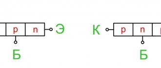
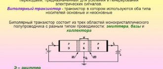
Bipolar transistors are more complex than semiconductor diodes; they have two pn junctions and three terminals called base, emitter and collector. There are two types of BT: NPN and PNP.
We will consider the device, features and circuitry using the example of NPN transistors - the most used in modern practice; for PNP transistors the reasoning is similar and the differences are only in connecting the supply voltages.
Design and principle of operation of bipolar transistors
The design and operating principle of NPN transistors are shown in Figure 2.19.
An NPN transistor has three microelectronic regions: two with N-conductivity and one with P-conductivity. Each area has a pin with the names indicated in the figure.
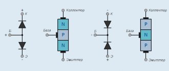
The structure of NPN-BT can also be represented in more understandable notations: as two diodes connected by anodes in the base area.
Figure 2.20 shows the most common way of using bipolar transistors, where the base and collector are applied at positive (+) potentials relative to the emitter. In this case, the positive potential of the collector is higher than the potential of the base! In other words, the collector pn junction is reverse biased (see, the collector diode is formally closed), and the base junction is forward biased.
Moreover, if a current is set into the base, then due to the structural feature of the bipolar transistor crystal, this base current Ib will “suck” electrons from the collector region and form a collector current
Ik= β*Ib, (2.7)
where β> 1 is called the base current gain.
Typical passport values β = 20÷500. The emitter current is thus in accordance with Kirchhoff's first law
Ie = (β +1)*Ib (2.8)
Linear mode of operation of bipolar transistors
In linear mode, the bipolar transistor amplifies the input signals.
The simplest transistor circuits that can be used to amplify low voltages are shown in Figure 2.21. Circuits of this configuration are usually called circuits (cascades) with a common emitter (OE circuits), because one of the BT terminals - the emitter, is used to generate both the input and output signals - is common to them. Let us explain the operation of such an amplifier.
Let the amplified signal be an alternating sinusoidal voltage that is supplied to the input of the common emitter circuit. The amplified signal is removed from the output of the OE circuit. The amplified signal has the same sine wave shape, but is out of phase with the input signal: as the input sine wave rises, the output sine wave falls.
The main characteristic of the amplifier is the input voltage gain, which is calculated as
Kus=ΔUout/ΔUin ≈ R2/re, (2.9)
where re is the emitter resistance. The emitter resistance can be calculated using the formula:
rе= ϕт/Iе = k*T/q*Iе ≈ k*T/q*Iк, (2.10)
where k is Boltzmann’s constant,
T – temperature in kelvins,
q – electron charge.
At a temperature of +25ºС (300 K) ϕt = 26 mV.
Notes
- There is a graphical way to estimate re. This requires knowledge of the input current-voltage characteristic of the selected bipolar transistor;
- The voltage gain of the signal, as can be seen from the formula, depends on temperature. In the case where the operating range of the amplifier circuit is wide, slightly more complex modifications of the combined emitter circuit are used, which are more resistant to temperature changes.
It should be borne in mind that the expression for Kus is approximate and it will be the more valid the larger β; it is good if β >100.
Calculation of the OE circuit for direct current
At this stage, we need to calculate the values of R1 and R2, which set the direct current mode, and R2 is also included in the expression for Kus.
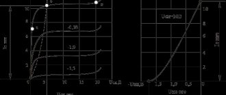
The operation of a bipolar transistor is described by its input and output characteristics (shown in Figure 2.22). The input characteristic Ib=ʄ(Ue), as one would expect, is similar to the characteristic of a semiconductor diode. However, for a transistor, the behavior of this characteristic also depends (slightly) on the voltage Uke. Therefore, in the technical descriptions for the selected transistor, families of input characteristics are given, where the parameter is Uke. The output characteristic is also a family of dependencies of the type Ik = ʄ (Uke), the parameter for which is the base current Ib.
Both families have fundamentally nonlinear behavior, however, this does not prevent them from being used for linear amplification. To do this, you need to build a load line on the output family, calculate the position of the operating point (PT) on it and determine the initial base current from the graph.
The load line is constructed, as before for the diode, between two similar points:
Ik=Epit/R2 and Uke=Epit. In our calculation, we set the values Epit = 15 V and Ik = Epit/R2 = 30 mA. Then R2=15/0.03 = 500 Ohm. We build a straight line and select the position of the RT - this is the middle of the linear section (shown in Figure 2.22). We will call the linear section the section of the load straight line between the saturation voltage and the cutoff voltage. The RT parameters in our example correspond to the following values (shown in Figure 2.23):
Uke.rt ≈ 7 V, Ik.rt ≈ 16 mA, Ib.rt ≈ 0.3 mA.
Next: we select from the family of input characteristics the characteristic that corresponds to the found value of Uke≈ 7.0 V, set Ib = 0.3 mA, and determine Ube≈ 0.65 V. We construct the actual section of the input load line and calculate R1 = (15- 0.65) V/ 0.3 mA = 45 kOhm.
Note – In practice, the calculation is somewhat more complicated.
Let's calculate the cascade gain at t°=25 °C.
Kus = Ie R2/ ϕt = 16 mA × 500 Ohm/ 26 mV ≈ 308.
It is important now to check whether the power dissipated on the collector does not exceed the nominal nameplate value of the selected bipolar transistor.
The calculation is carried out at the operating point: Uke.rt ×Ik.rt = 7 V × 16 mA = 112 mW. This value is constant and does not change in the input signal amplification mode, when the collector voltages and currents vary over a wide range. This is explained by the fact that the collector voltage and current change in antiphase in this circuit: when the current increases, the voltage decreases, and vice versa.
Calculation of the OE circuit for alternating current
An example of the generation of output signals from a circuit with an OE under the influence of a change in the base current is shown in Figure 2.23. Under the influence of a sinusoidally varying base current (sinusoid depicted by a dotted line), the RT shifts along the load line, first up to its maximum, and then down to its minimum.
From the figure we see that when the base current changes in the range from 0.05 to 0.55 mA with an amplitude of (0.55-0.05)/2 = 250 μA, the collector current changes in the range from approximately 3 mA to 29 mA s amplitude (29-3)/2 = 13 mA. From here we have the following value of the current gain:
Ki= 13,000/250 = 52
The collector voltage varies in the range from approximately 0.5 V to 13 V with an amplitude of (13-0.5)/2 = 6.25 V. Let us emphasize once again that the change in the collector voltage is carried out in antiphase with the change in the input (amplified) current: When the base current increases, the collector current increases and the collector voltage decreases!
So far we have not said anything about capacitors C1 and C2. These are so-called coupling capacitors. They do not transmit constant components of amplified voltages and only transmit variable ones. Their values should be large enough: the larger the capacitance values, the lower ʄn - the minimum amplified frequency. Typically these capacitors have values between 1 and 100 µF.
Measuring the current gain of a bipolar transistor
If the tester has the ability to measure the current transfer coefficient, then you can check the operation of the transistor by installing the transistor leads into the corresponding sockets.
We recommend reading: How to calculate the resistance of a resistor to reduce current
Current transfer coefficient is the ratio of the collector current to the base current.
The higher the gain, the more collector current can be controlled by the base current, all other things being equal.
The pinout (pin name) and other data can be taken from the data sheets (reference data) for the corresponding transistor. Data sheets can be found on the Internet through search engines.
The tester will show on the display the current transfer (gain) coefficient, which must be compared with the reference data.
The current transfer coefficient of low-power transistors can reach several hundred.
For powerful transistors it is significantly smaller - several units or tens.
However, there are powerful transistors with a transfer coefficient of several hundred or thousand. These are the so-called Darlington pairs.
A Darlington pair consists of two transistors. The output current of the first transistor is the input current for the second.
The overall current transfer coefficient is the product of the coefficients of the first and second transistors.
The Darlington pair is made in a common housing, but it can also be made from two separate transistors.
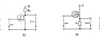
Key operating mode of bipolar transistors
Let's look at the output characteristics of the BT. When a large current is supplied to the base (>0.3 mA), the voltage Uke decreases to its minimum value (typical value 0.2 V). They say “the transistor goes into saturation mode.”
On the other hand, if no current is supplied to the base (Ib ~ 0), then the collector current is interrupted and the voltage at the output of the cascade will be equal to the supply voltage Epi - the bipolar transistor will be in “cut-off mode”.
Actually, these two states of the BT describe the key mode of its operation: the switch (transistor) is on or off, the load is connected to the power supply or is disconnected. The simplest key circuits on BT are shown in Figure 2.24. The presented circuit diagrams show that the circuits are controlled using digital signals: logical zero (“0”) and logical one (“1”). In modern practice, such signals are most often generated by microcontrollers.
Please note that both types of BT are used in circuits with positive (+Epit) power supply and the load in both cases is located in the collector circuit of the BT. In this case: a logical unit in one of the cases (NPN transistor) closes the switch, and in the other (PNP transistor) it opens it.
Key closure condition: Ib * β >Ik.us ≈ Epit/Rload. The base current can be approximately calculated for both cases as follows: Ib = (Epit-0.6)/R1.
Knowing the supply voltage, load resistance and base current amplification factor β, R1 can be calculated using the indicated formulas.
Types of transistors
Based on their operating principle and structure, semiconductor triodes are distinguished:
- field;
- bipolar;
- combined.
These transistors perform the same functions, but there are differences in the principle of their operation.
Field
This type of triode is also called unipolar, due to its electrical properties - they carry current of only one polarity. Based on their structure and type of control, these devices are divided into 3 types:
- Transistors with control pn junction (Fig. 6).
- With an insulated gate (available with a built-in or induced channel).
- MIS, with structure: metal-dielectric-conductor.
A distinctive feature of an insulated gate is the presence of a dielectric between it and the channel.
Parts are very sensitive to static electricity.
Circuits of field triodes are shown in Figure 5.
Rice. 5. Field effect transistors
Rice. 6. Photo of a real field-effect triode
Pay attention to the names of the electrodes: drain, source and gate.
Field effect transistors consume very little power. They can work for more than a year on a small battery or rechargeable battery. Therefore, they are widely used in modern electronic devices such as remote controls, mobile gadgets, etc.
Bipolar
Much has been said about this type of transistor in the subsection “Basic operating principle.” Let us only note that the device received the name “Bipolar” because of its ability to pass charges of opposite signs through one channel. Their feature is low output impedance.
Transistors amplify signals and act as switching devices. A fairly powerful load can be connected to the collector circuit. Due to the high collector current, the load resistance can be reduced.
Let's look at the structure and principle of operation in more detail below.
Combined
In order to achieve certain electrical parameters from the use of one discrete element, transistor developers invent combined designs. Among them are:
- bipolar transistors with embedded resistors and their circuit;
- combinations of two triodes (same or different structures) in one package;
- lambda diodes - a combination of two field-effect triodes forming a section with negative resistance;
- designs in which a field-effect triode with an insulated gate controls a bipolar triode (used to control electric motors).
Combined transistors are, in fact, an elementary microcircuit in one package.
Checking the performance of bipolar transistors
Many multimeters allow you to measure the base current gain (β; h21) of transistors with flexible leads. Figure 2.26 shows a typical solution to this problem. A transistor is connected to a special connector, following the order indicated on the front panel. The β value appears on the display.
Notes
- NPN and PNP transistors have separate sockets for connection.
- For both types of transistors, two sockets are provided for connecting the emitter. This is due to possible design differences in the pinouts of the transistors.
What is a transistor?
A transistor is an electronic semiconductor device designed to amplify, generate and convert electrical signals. To be more precise, the transistor allows you to regulate the strength of the electric current, just as a water faucet regulates the flow of water. This leads to two main functions of the device in an electrical circuit - an amplifier and a switch.
There are an infinite number of different types of transistors - from huge high-power amplifiers the size of a fist, to miniature switches on a processor chip measuring just tens of nanometers (there are 109 nanometers in one meter).