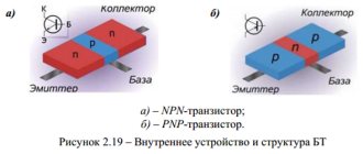
Bipolar transistor
A semiconductor device consists of three layers of different conductivity, each of which is connected to conductive contacts.
The collector, base and emitter layers differ little in the degree of electrical conductivity, but during production they are subject to different levels of doping:
- The first is lightly doped, which makes it possible to increase the collector voltage.
- Many impurities are added to the emitter during manufacturing. The amount of reverse breakdown voltage does not become critical, since the devices operate with a forward-biased junction. Increased doping results in increased injection of secondary charge carriers into the base layer.
The base layer is lightly doped, since it is located between the collector and the emitter, this layer should show high resistance.
How does it work
Charge carriers move to the collector through a thin base layer. The middle layer is separated from the upper and lower pn junctions.
Features of operation:
- Current flows through the transistor if charging carriers are injected through the pn junction into the base layer from the emitter layer.
- The result is a reduction in potential obstruction when applying forward bias.
- In the base layer, the injected charges are not the majority carriers, therefore they are accelerated and enter other pn junctions to the collector layer from the base layer.
- In the base, charges spread under the influence of diffusion or electric field.
Transistor efficiency improves if a thin base layer is used, but excessive thinning reduces the collector voltage limit.
Connection diagram
The transistor has three terminals for installation in a circuit. When connected, one contact is defined as common.
There are connection schemes:
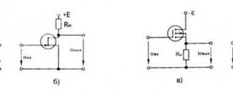
- With joint emitter. A commonly used circuit amplifies the current and voltage (showing the greatest power increase). The input pulse arrives at the base layer from the emitter side, is removed from the collector and is inverted.
- With a joint collector. Only the electric current increases, the voltage gain is 1, the input resistance is high and the output resistance is low. The connection supports a wide range of amplified frequencies.
If the base layer is common when connected, the voltage increases, so it is used more often in composite systems, but not in single-transistor ones.
Recommendations for using transistors
The values of most transistor parameters depend on the actual operating mode and temperature, and with increasing temperature, the transistor parameters may change. The reference book contains, as a rule, typical (averaged) dependences of transistor parameters on current, voltage, temperature, frequency, etc.
To ensure reliable operation of transistors, it is necessary to take measures to exclude long-term electrical loads close to the maximum permissible. For example, replacing a transistor with a similar one but of lower power is not worth it; this applies not only to power, but also to other parameters of the transistor. In some cases, to increase power, transistors can be connected in parallel, with emitter connected to emitter, collector to collector, and base to base. Overloads can be caused by various reasons, for example from overvoltage; high-speed diodes are often used to protect against overvoltage.
As for heating and overheating of transistors, the temperature regime of transistors not only affects the value of the parameters, but also determines the reliability of their operation. You should strive to ensure that the transistor does not overheat during operation; in the output stages of amplifiers, transistors must be placed on large radiators. Transistors must be protected from overheating not only during operation, but also during soldering. When tinning and soldering, measures should be taken to prevent overheating of the transistor; it is advisable to hold the transistors with tweezers during soldering to protect them from overheating.
We have looked at only a few types of transistors here, and this is only a tiny part of the abundance of models of electronic components on the market today.
One way or another, you can easily choose the appropriate transistor for your purposes. Documentation for them is available today on the Internet in the form of datasheets, which comprehensively present all the characteristics. The package types of modern transistors are different, and both SMD and lead-out versions are often available for the same model.
Field-effect transistor
The purpose is the same as bipolar, but the structure is different. Transistors coordinate higher powers in similar sizes.
The structure contains elements:
- drain for receiving high voltage;
- gate for controlled voltage;
- source for distributing voltage in the open position.
Valera
The voice of the construction guru
Ask a Question
There are field-type devices: with control via a pn junction, with an electrically insulated gate. In the first case, on opposite sides of the semiconductor, areas of different electrical conductivity are obtained to control the electric current. In the second type, the gate is separated from the channel by a dielectric material.
How does it work
In a field-effect device, current flows to the drain through a channel in the doped conductor under the gate. It is located between the undoped layer (there are no charging carriers in it) and the gate. There is a depletion region here where no current is conducted.
The width of the channel is limited by the area between the depletion region and the interlayer. The current is controlled by changing the voltage applied to the gate. In this case, the channel cross-section changes, and the output current changes its value.
Connection schemes
Field-effect transistors are connected in one of three ways:
- with common drain;
- with a common source;
- with a common base.
The circuit with a common drain is similar to connecting a bipolar module with a common collector. This type of connection is used in matching cascades, where a high input voltage is needed and a low output voltage. The inclusion supports a wide range of frequencies.
The common source circuit produces a large increase in power and current, while the phase of the drain circuit voltage is reversed. The input resistance can be several hundred megaohms; to reduce it, a resistor is added between the source and gate.
In a circuit with a common gate, there is no amplification of the electric current, the increase in power is small. The voltage is in a similar phase with the control one. When the input pulse changes, the voltage at the source increases or decreases.
Comparison with regular elements
Remember when we repaired the computer motherboard and changed capacitors and field-effect transistors? These are large enough elements on which the markings can be read with the naked eye. The capacitors in the low-voltage voltage regulator of the processor core on the motherboard cannot be made very small. To properly filter pulsations, they must have a capacity of several hundred microfarads. You can’t squeeze such a container into a small volume.
It will be interesting➡ What are rectifier diodes needed for?
The field-effect transistors in this stabilizer also cannot be made very small. Currents of tens of amperes flow through them. Field-effect transistors with a very low open-channel resistance are used - tenths and hundredths of an Ohm. But at such currents they can dissipate power of half a watt or more. The flow of current through an open channel causes the transistor to heat up. The heat is radiated into the surrounding space through the area of the transistor housing. If the package is very small, the transistor will not be able to dissipate heat and will burn out.
By the way, please note: field-effect transistors are soldered by the body to the pads of the printed circuit board. Copper pads conduct heat well, so heat dissipation is more efficient. But there are components on the same motherboard that do not carry large currents and do not dissipate much power. Therefore they can be made very small. If we look inside a computer power supply, we will see very small capacitors and resistors. They are used in control and feedback circuits.
Useful material: what is a semiconductor diode.
Such elements look like a cylinder or brick with thin wire leads. Installation of these components is carried out in the traditional way: through holes in the board, the element is soldered with leads to the contact pads of the board. This technology was mastered decades ago. E
The disadvantage is that tens or hundreds of holes need to be drilled in the board. This is not the simplest technological operation. To get rid of drilling (or reduce the number of holes) and reduce the size of finished products, SMD components were invented. Computer motherboards contain both conventional lead wire elements and SMD components. There are more of the latter.
Combined transistors
A hybrid of a field and bipolar device has the positive features of both devices. The bottom line is that a high-power bipolar transistor is controlled by a field effect transistor . A large load can be changed using low power, since the control pulse is applied to the gate of the field-type device.
The internal structure of combined transistors is a cascade connection of two input switches to adjust the final plus. When a positive voltage is applied from the source to the gate, the field type begins to operate, and a transmission channel appears between the source and drain.
The movement of charging carriers between sections of pn junctions turns on the bipolar device, so the electric current moves to the collector from the emitter.
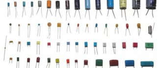
What SMD components look like
It is interesting to note that the soldering reliability of lead-free solder is lower than that of lead-containing solders. Therefore, the RoHS Directive does not apply in particular to military products and active implantable medical devices. SMD diodes and zener diodes look like bricks with very short leads (0.5 mm or less), or like cylinders with metallized ends. SMD transistors come in packages of various sizes and configurations.
It will be interesting➡ What are field-effect transistors?
For example, SOT23 and DPAK packages are widely used. The terminals can be located on one or both sides of the housing. Surface mount microcircuits can be divided into two large classes. The first has pins located on the sides of the case parallel to the surface of the board. Such enclosures are called planar. The leads can be on two long sides or on all four sides. For microcircuits of another class, the conclusions are made in the form of hemispheres at the bottom of the case.
The most common transistor model.
As a rule, large microcircuits (chipsets) are made in such cases on computer motherboards or video cards. It is interesting to note that traditional elements were first digitally marked. Resistors, for example, were marked with type, nominal resistance value and deviation.
Then they began to use markings in the form of colored rings or dots. This made it possible to mark the smallest elements. SMD elements use alphanumeric (where the standard size allows) and color markings.
Related material: How to connect a capacitor