The first state “off” (transistor closed) is determined by point A1 on the output characteristics of the transistor; it is called cutoff mode. In the cutoff mode, the base current Ib = 0, the collector current Ik1 is equal to the initial collector current, and the collector voltage Uk = Uk1 ≈ Ek. The cutoff mode is implemented at Uin = 0 or at negative base potentials. In this state, the switch resistance reaches its maximum value: Rmax = , where RT is the transistor resistance in the closed state, more than 1 MOhm.
The second state “on” (the transistor is open) is determined by point A2 on the current-voltage characteristic and is called the saturation mode. From the cutoff mode (A1) to the saturation mode (A2), the transistor is switched by a positive input voltage Uin. In this case, the voltage Uout takes the minimum value Uk2 = Uk.e.us of the order of 0.2-1.0 V, the collector current Ik2 = Ik.us ≈ Ek/Rk. The base current in saturation mode is determined from the condition: Ib > Ib.us = Ik.us / h21.
The input voltage required to switch the transistor to the open state is determined from the condition: Uin > Ib.us · Rb + Uk.e.us
Good noise immunity and low power dissipation in the transistor are explained by the fact that most of the time the transistor is either saturated (A2) or closed (A1), and the transition time from one state to another is a small part of the duration of these states. The switching time of switches on bipolar transistors is determined by the barrier capacitances of the p-n junctions and the processes of accumulation and resorption of minority charge carriers in the base.
To increase speed and input resistance, field-effect transistor switches are used.
Switch circuits on field-effect transistors with a control pn junction and with an induced channel with a common source and common drain are shown in the figure:
For any switch on a field-effect transistor Rн > 10-100 kOhm.
The control signal Uin at the gate is about 10-15 V. The resistance of the field-effect transistor in the closed state is high, about 108-109 Ohms.
The resistance of the field-effect transistor in the open state can be 7-30 Ohms. The resistance of the field-effect transistor along the control circuit can be 108-109 Ohms. (schemes “a” and “b”) and 1012-1014 Ohms (schemes “c” and “d”).
Top
Operating principle of NPN transistor
In its modern meaning, a transistor is a semiconductor radio element designed to change the parameters of an electric current and control it.
A conventional semiconductor triode has three terminals: a base, which receives control signals, an emitter, and a collector. There are also high power composite transistors. The size scale of semiconductor devices is striking - from several nanometers (unpackaged elements used in microcircuits) to centimeters in diameter for high-power transistors intended for power plants and industrial equipment. Reverse voltages of industrial triodes can reach up to 1000 V.
Operating principle
The basis of the device’s operation is the ability of the np junction to pass current in one direction. When voltage is applied, a forward drop occurs at one junction, and a reverse drop at the other. The transition zone with direct voltage has low resistance, and with reverse voltage it has high resistance. A small control current flows between the base and emitter. The value of this current changes the resistance between the collector and emitter.
There are two types of bipolar device:
- pnp;
- npn.
The only difference is in the main charge carriers, i.e., the direction of the current.
If you connect two semiconductors of different types to each other, then at the boundary of the connection a region appears, or, as is commonly called, a pn junction. The type of conductivity depends on the atomic structure of the material, namely how strong the bonds in the material are. The atoms in a semiconductor are arranged in a lattice, and the material itself is not a conductor. But if atoms of another material are added to the lattice, the physical properties of the semiconductor change. Mixed atoms form, depending on their nature, free electrons or holes.
The free electrons formed form a negative charge, and the holes form a positive charge. There is a potential barrier in the transition area. It is formed by a contact potential difference, and its height does not exceed tenths of a volt, preventing the flow of charge carriers deep into the material. If the junction is under direct voltage, then the magnitude of the potential barrier decreases, and the magnitude of the current passing through it increases. When a reverse voltage is applied, the magnitude of the barrier increases and the barrier's resistance to the passage of current increases. By understanding the operation of a pn junction, you can understand how a transistor works.
Connection schemes
To correctly use and connect BTs, you need to know their classification and type. Classification of bipolar transistors:
- Materials of manufacture: germanium, silicon and gallium arsenide.
- Manufacturing features.
- Power dissipation: low power (up to 0.25 W), medium (0.25-1.6 W), high power (above 1.6 W).
- Limit frequency: low-frequency (up to 2.7 MHz), mid-frequency (2.7-32 MHz), high-frequency (32-310 MHz), ultra-high-frequency (more than 310 MHz).
- Functional purpose.
The functional purpose of BT is divided into the following types:
- Low-frequency amplification with normalized and non-standardized noise figure (NiNNKSh).
- High-frequency amplification with NiNNKSh.
- Micro-frequency amplification with NiNNKSh.
- Powerful high-voltage amplifiers.
- Generator with high and ultra-high frequencies.
- Low-power and high-power high-voltage switching switches.
- Pulse powerful for working with high U values.
In addition, there are the following types of bipolar transistors:
- P-np.
- Npn.
There are 3 circuits for switching on a bipolar transistor, each of which has its own advantages and disadvantages:
- General B.
- General E.
- General K.
Features of the transistor device
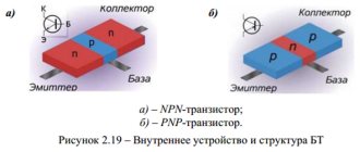
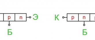
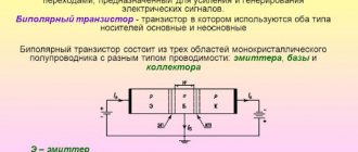
The NPN transistor includes three regions:
- emitter;
- the base is very thin, which is made of a lightly doped semiconductor, the resistance of this area is high;
- collector - its area is larger in size than the emitter area.
Metal contacts are soldered to each area, which serve to connect the device to the electrical circuit.
The collector and emitter conductivities are the same and opposite to the base conductivities. In accordance with the type of conductivity of the areas, pnp or npn devices are distinguished. The devices are asymmetrical due to the difference in contact area - between the emitter and base it is much lower than between the base and collector. Therefore, it is impossible to swap K and E by changing polarity.
Bipolar microwave transistor [edit | edit code ]
Microwave bipolar transistors (Microwave Bipolar Transistors) are used to amplify oscillations with frequencies above 0.3 GHz [7]. The upper limit of BT microwave frequencies with an output power of more than 1 W is about 10 GHz. Most powerful microwave BTs are of the npn type in structure [8]. According to the method of formation of transitions, BT microwaves are epitaxial-planar. All microwave BTs, except the lowest-power ones, have a multi-emitter structure (comb, mesh) [9]. Based on power, BT microwaves are divided into low-power (dissipated power up to 0.3 W), medium-power (from 0.3 to 1.5 W) and high-power (over 1.5 W) [10]. A large number of highly specialized types of microwave BTs are produced [10].
Transistor operating modes
So, we have looked at the active mode of operation of the transistor (emitter-base junction is open, collector-base junction is closed), we will not ignore others
Cutoff mode. Both pn junctions are closed. Moreover, it is important to note that the emitter-base junction opens starting from a certain value of the applied forward voltage (not from zero). This voltage is usually about 0.6 V. That is, in the cutoff mode, either both junctions are reverse biased, or the collector junction is reverse biased, and the emitter junction is forward biased, but the voltage value does not exceed 0.6 V.
In this mode, the transitions are greatly depleted of free charge carriers and the current flow almost completely stops. The only exceptions are small side currents of transitions. In an ideal case (without leakage currents), a transistor in cutoff mode is equivalent to an open circuit.
Saturation mode. Both junctions are open, and as a result, majority charge carriers actively move from the collector and emitter to the base. An excess of charge carriers appears in the base, its resistance and the resistance of pn junctions decreases and current begins to flow between the emitter and collector. Ideally, a transistor in this mode is equivalent to closing the circuit.
Barrier mode. We will definitely look at it in more detail; in short, the idea is that the base is connected directly or through a small resistance to the collector. This is equivalent to using a diode with a resistor in series.
That's all the most basic operating modes of a bipolar transistor!
Transistor operating principle
Now we will try to figure out how a transistor works. I will not go into details of the internal structure of transistors as this information will only confuse. Better take a look at this drawing.
This image best explains the working principle of a transistor. In this image, a person controls the collector current using a rheostat. He looks at the base current; if the base current increases, then the person also increases the collector current, taking into account the gain of the transistor h21E. If the base current drops, then the collector current will also decrease - the person will correct it using a rheostat.
It will be interesting➡ Vacuum switch: device and principle of operation + nuances of selection and connection
This analogy has nothing to do with the actual operation of a transistor, but it makes it easier to understand the principles of its operation.
For transistors, rules can be noted to help make things easier to understand. (These rules are taken from the book “The Art of Circuit Design” by P. Horowitz W. Hill).
- The collector has a more positive potential than the emitter
- As I already said, the base-collector and base-emitter circuits work like diodes
- Each transistor is characterized by limiting values such as collector current, base current and collector-emitter voltage.
- If rules 1-3 are followed, then the collector current Ik is directly proportional to the base current Ib. This relationship can be written as a formula.
From this formula we can express the main property of a transistor - a small base current controls a large collector current.
- current gain.
It is also denoted as
Based on the above, the transistor can operate in four modes:
- Transistor cutoff mode - in this mode, the base-emitter junction is closed, this can happen when the base-emitter voltage is insufficient. As a result, there is no base current and therefore there will be no collector current either.
- The active mode of a transistor is the normal mode of operation of the transistor. In this mode, the base-emitter voltage is sufficient to cause the base-emitter junction to open. The base current is sufficient and the collector current is also available. The collector current is equal to the base current multiplied by the gain.
- Transistor saturation mode - the transistor enters this mode when the base current becomes so large that the power of the power source is simply not enough to further increase the collector current. In this mode, the collector current cannot increase following an increase in the base current.
- Inverse transistor mode - this mode is used extremely rarely. In this mode, the collector and emitter of the transistor are swapped. As a result of such manipulations, the gain of the transistor suffers greatly. The transistor was not originally designed to operate in such a special mode.
To understand how a transistor works, you need to look at specific circuit examples, so let's look at some of them.
Transistor in switch mode
A transistor in switch mode is one of the cases of transistor circuits with a common emitter. The transistor circuit in switching mode is used very often. This transistor circuit is used, for example, when it is necessary to control a powerful load using a microcontroller. The controller leg is not capable of pulling a powerful load, but the transistor can. It turns out that the controller controls the transistor, and the transistor controls a powerful load. Well, first things first.
The main idea of this mode is that the base current controls the collector current. Moreover, the collector current is much greater than the base current. Here you can see with the naked eye that the current signal is amplified. This amplification is carried out using the energy of the power source.
The figure shows a diagram of the operation of a transistor in switching mode.
For transistor circuits, voltages do not play a big role, only currents matter. Therefore, if the ratio of the collector current to the base current is less than the gain of the transistor, then everything is okay.
In this case, even if we have a voltage of 5 volts applied to the base and 500 volts in the collector circuit, then nothing bad will happen, the transistor will obediently switch the high-voltage load.
The main thing is that these voltages do not exceed the limit values for a specific transistor (set in the transistor characteristics).
Well, now let's try to calculate the value of the base resistor.
As far as we know, the current value is a characteristic of the load.
Those. I=U/R
We don't know the resistance of the light bulb, but we know the operating current of the light bulb is 100 mA. In order for the transistor to open and allow such current to flow, you need to select the appropriate base current. We can adjust the base current by changing the value of the base resistor.
Since the minimum value of the transistor gain is 10, then for the transistor to open, the base current must become 10 mA.
The current we need is known. The voltage across the base resistor will be This voltage value across the resistor is due to the fact that 0.6V-0.7V is dropped at the base-emitter junction and we must not forget to take this into account.
As a result, we can easily find the resistance of the resistor
All that remains is to choose a specific value from a number of resistors and it’s done.
Now you probably think that the transistor switch will work as it should? That when the base resistor is connected to +5 V the light bulb lights up, when it is turned off the light bulb goes out? The answer may or may not be yes.
The thing is that there is a small nuance here.
The light bulb will go out when the resistor potential is equal to the ground potential. If the resistor is simply disconnected from the voltage source, then everything is not so simple. The voltage on the base resistor can miraculously arise as a result of interference or some other otherworldly evil spirit
To prevent this effect from happening, do the following. Another resistor Rbe is connected between the base and emitter. This resistor is chosen with a value at least 10 times larger than the base resistor Rb (In our case, we took a 4.3 kOhm resistor).
It will be interesting➡ What is an oscilloscope and what is it for?
When the base is connected to any voltage, the transistor works as it should, the resistor Rbe does not interfere with it. This resistor consumes only a small portion of the base current.
In the case when voltage is not applied to the base, the base is pulled up to the ground potential, which saves us from all kinds of interference.
So, in principle, we have figured out the operation of the transistor in the key mode, and as you can see, the key mode of operation is a kind of voltage amplification of the signal. After all, we controlled a voltage of 12 V using a low voltage of 5V.
Emitter follower
An emitter follower is a special case of common-collector transistor circuits.
A distinctive feature of a circuit with a common collector from a circuit with a common emitter (option with a transistor switch) is that this circuit does not amplify the voltage signal. What went in through the base came out through the emitter, with the same voltage.
Indeed, let’s say we applied 10 volts to the base, while we know that at the base-emitter junction somewhere around 0.6-0.7V is dropped. It turns out that at the output (at the emitter, at the load Rн) there will be a base voltage of minus 0.6V.
It turned out 9.4V, in a word, almost as much as went in and out. We made sure that this circuit will not increase the voltage for us.
“What is the point then of turning on the transistor like this?” you ask. But it turns out that this scheme has another very important property. The circuit for connecting a transistor with a common collector amplifies the signal in terms of power. Power is the product of current and voltage, but since the voltage does not change, the power increases only due to the current! The load current is the sum of the base current plus the collector current. But if you compare the base current and the collector current, the base current is very small compared to the collector current. It turns out that the load current is equal to the collector current. And the result is this formula.
Now I think it’s clear what the essence of the emitter follower circuit is, but that’s not all.
The emitter follower has another very valuable quality - high input impedance. This means that this transistor circuit consumes almost no input current and creates no load on the signal source circuit.
To understand the principle of operation of a transistor, these two transistor circuits will be quite sufficient. And if you experiment with a soldering iron in your hands, the epiphany simply won’t keep you waiting, because theory is theory, and practice and personal experience are hundreds of times more valuable!
Calculation of base input current Ib
Now let's calculate the base current Ib. Since we are dealing with alternating voltage, we need to calculate two current values - at the maximum voltage (Vmax) and minimum (Vmin). Let's call these current values Ibmax and Ibmin, respectively.
Also, in order to calculate the base current, you need to know the base-emitter voltage VBE. There is one PN junction between the base and emitter. It turns out that the base current “meets” the semiconductor diode on its path. The voltage at which a semiconductor diode begins to conduct is about 0.6V. We will not go into details of the current-voltage characteristics of the diode, and for simplicity of calculations we will take an approximate model, according to which the voltage on the current-carrying diode is always 0.6V. This means that the voltage between base and emitter VBE = 0.6V. And since the emitter is connected to ground (VE = 0), the voltage from base to ground is also 0.6V (VB = 0.6V).
Let's calculate Ibmax and Ibmin using Ohm's law:
Calculation of a switch for a transistor
Let's add a payload in the form of an LED to the circuit. Resistor R_k remains in place, it will limit the current through the load and ensure the required operating mode:
Suppose that to turn on the LED you need to apply a voltage of 3V (U_d) to it. In this case, the diode will consume a current equal to 50 mA (I_d). Let's set the transistor parameters (in real circuits, these values are taken from the documentation for the transistor used):
- Current gain h_{21e} = 100…500 (the range is always specified, not a specific value)
- The voltage drop across the base-emitter junction required to open this junction: U_{be} = 0.6 medspace V.
- Saturation voltage: U_{ke medspace us} = 0.1 medspace V.
We take specific values for calculations, but in practice everything is somewhat different. As you remember, the parameters of transistors depend on many factors, in particular on the operating mode, as well as on temperature. And the ambient temperature, of course, can change. It is not so easy to determine clear values from the characteristics, so you need to try to ensure a small margin. For example, when calculating, it is better to take the current gain equal to the minimum of the values given in the datasheet. After all, if the coefficient in reality is higher, then this will not disrupt the operation of the circuit; of course, the efficiency will be lower, but nevertheless the circuit will work. And if we take the maximum value of h_{21e}, then under certain conditions it may turn out that the real value turned out to be less, and it is no longer sufficient to ensure the required operating mode of the transistor.
So, let's return to the example. The input data for the calculation, among other things, are the voltages of the sources. In this case:
- E_{in} = 3.3medspace Q. I chose a typical value that is found in practice when developing circuits on microcontrollers. In this example, this voltage is turned on and off by switch S_1.
- E_{out} = 9medspace B.
First of all, we need to calculate the resistance of the resistor in the collector circuit. The voltages and currents of the output circuit in the on state are related as follows:
U_{ke medspace us} + U_{R_k} + U_d = E_{out}
In this case, according to Ohm's law:
U_{R_к} = I_к R_к
And we have a given current, since we know how much current the load (in this case, a diode) consumes when it is on. Then:
U_{R_k} = I_d R_kU_{ke medspace us} + I_d R_k + U_d = E_{out}
So, in this formula we know everything except the resistance, which needs to be determined:
R_к = frac{E_{out} medspace — medspace U_д medspace — medspace U_{ке medspace us}}{I_д} enspace= frac{9 medspace B medspace — medspace 3 medspace B medspace — medspace 0.1 medspace B}{0.05 medspace A} medspaceapprox 118 medspace Ohm.
It will be interesting➡ What is a magnetic starter + installation diagrams
We select an available resistance value from the standard range of ratings and get R_{к} = 120medspace Ohm. Moreover, it is important to choose a larger value. This is due to the fact that if we take a value slightly larger than calculated, then the current through the load will be slightly less. This will not lead to any malfunctions. If you take a smaller resistance value, this will lead to the fact that the current and voltage at the load will exceed the specified ones, which is worse
Let's recalculate the collector current value for the selected resistance value:
I_к = frac{U_{R_к}}{R_к} medspace = frac{9 medspace V medspace — medspace 3 medspace V medspace — medspace 0.1 medspace V}{120 medspace Ohm} medspaceapproxmedspace 49.17 medspace mA
It's time to determine the base current; for this we use the minimum gain value:
I_b = frac{I_к}{h_{21е}} = frac{49.17 medspace mA}{100} = 491.7 medspace μA
And the voltage drop across resistor R_b:
U_{R_b} = E_{in} medspace — medspace 0.6 medspace B = 3.3 medspace B medspace — medspace 0.6 medspace B = 2.7 medspace B
Now we can easily determine the resistance value:
R_b = frac{U_{R_b}}{I_b}medspace = frac{2.7 medspace V}{491.7 medspace μA} approx 5.49 medspace KOhm
Again we turn to a number of acceptable denominations. But now we need to choose a value less than the calculated one. If the resistor resistance is greater than the calculated value, then the base current will, on the contrary, be less. And this can lead to the fact that the transistor does not open completely, and when it is on, most of the voltage will drop across the transistor (U_{ke}), which, of course, is undesirable.
Therefore, we select a value of 5.1 KOhm for the base resistor. And this stage of calculation was the last! Let's recap, our calculated denominations were:
- R_{b} = 5.1medspace KOhm
- R_{k} = 120medspace Ohm
By the way, in a transistor switch circuit, a resistor is usually added between the base and emitter, with a nominal value of, for example, 10 KOhm. It is needed to tighten the base when there is no signal at the input. In our example, when S1 is open, the input simply hangs in the air. And under the influence of interference, the transistor will randomly open and close. Therefore, a pull-up resistor is added so that in the absence of an input signal, the base potential is equal to the emitter potential. In this case, the transistor will be guaranteed to be closed.
Today we went through the classical scheme, which I try to adhere to, that is, from theory to practice. I hope that the material will be useful, and if you have any questions, write in the comments, I will be happy to help!
Characteristics of a transistor connected according to the circuit
Only diffusion movement of electrons occurs through the base, since there is no action of the electric field there. The transistor has only three terminals, so to implement a four-terminal network, one of the terminals must be connected to both the input and output of the amplifier. A positive type of charge, or hole, is formed at the site of the released electron. The power supply voltage and load must remain the same for both measurements.
Conclusion Semiconductor elements are used in electrical signal conversion circuits. Although the transition layers are based on the same principle, the transistor is an asymmetrical device. The active mode of a transistor is the normal mode of operation of the transistor. In this case, the transistor parameters do not play any role here at all. Firstly, the gain of the cascade depends on the specific instance of the transistor: if you replaced the transistor during repair, select the bias again, bring it to the operating point.
If the base current drops, then the collector current will also decrease - the person will correct it using a rheostat.
The operation of the amplifier is clearly visible in the timing diagrams. Figure 2. How does a transistor work? TTL logic / Gain mode. Animated educational 2D video. / Lesson 1