AudioKiller's site
Feedback is the process of transmitting a signal from the output of an amplifier back to its input, as well as the circuit that carries out this transmission.
Feedback (Feedback) is called negative ( NFB ), if the output signal of the amplifier is subtracted from the input signal. For simplicity, we will consider the steady-state operating mode of the entire system, with the amplifier operating in the active mode (i.e., it normally amplifies the signal without any overloads).
The block diagram of an amplifier covered by OOS is shown in Fig. 1.
Rice. 1. Block diagram of an amplifier covered by OOS.
Here, some “virtual” amplifier with voltage gain Ku' is obtained from the original “real” amplifier, which has gain Ku, and is covered by the feedback loop. In fact, the term “virtual” is not entirely correct, but I will use it because from the point of view of external devices connected to the system as a whole, it is an amplifier with parameters that differ from the parameters of the real original amplifier without OOS.
From the output of a real amplifier, the voltage is transmitted to its input through an OOS circuit with a transfer coefficient β:
Usually the OOS circuit is passive, and β ≤ 1. If the OOS circuit amplifies, then this does not fundamentally change anything, and all formulas in this case are derived similarly. If β = 0, then this means that Uoos = 0 and there is no feedback. Please note that it makes no difference what kind of circuit the OOS circuit has. The main thing is how much (how many times) it relieves tension.
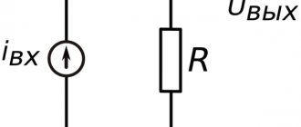
There are two different input voltages in this system, and to avoid confusion, I will give them different names:
1. Voltage supplied to the input of the “virtual” amplifier from the signal source. We will denote it as Usign.
2. The voltage coming to the input of a real amplifier is Uin.
So, the output voltage of the amplifier Uout is converted by the OOS circuit into the feedback voltage Uoos and subtracted from the input voltage. The result is the input voltage of a real amplifier:
An important point: Uoos is always less than Usign, so Uin is always greater than zero.
A real amplifier amplifies its input signal by Ku times:
Let's transform formula (3):
But Uout/Usign is the gain Ku' of the “virtual” amplifier as it appears to the outside world, therefore:
Thus, we have obtained a formula for calculating the gain for an amplifier covered by OOS.
Now we can explain why Uoos < Usign. Let us assume that Uoos = Usign. Then the voltage coming to the input of a real amplifier is zero: Uin = Usign – Uoos = 0. And if so, then the output voltage of the amplifier is zero: Uout = Uin∙Ku. But Uoos is obtained from the output voltage: Uoos = Uout∙β, which means it will also be equal to zero! We came to a contradiction: assuming that Uoos = Usign, we found that Uoos = 0. This happens only when there is no signal at the input of the entire system, when all voltages are equal to zero. What will happen if Uoos > Usign, consider for yourself. From the point of view of mathematics, the initial statement can be proven in an elementary way:
When considering the physics of processes, it should be remembered that the output voltage of the amplifier does not appear on its own, but is a consequence of its amplification and is formed from its input voltage: Uout = Ku∙Uin.
So, when the amplifier is covered by OOS, its gain decreases by (1+β∙Ku) times. But the introduction of OOS also changes other parameters of the amplifier.
1. Negative feedback changes the input and output resistance of the amplifier by (1+β∙Ku) times. Moreover, they can either increase or decrease depending on the method of connecting the OOS circuit to the input and output of the amplifier - in series or in parallel. Methods for connecting the OOS circuit to the amplifier input are shown in Fig. 2, and to the amplifier output - in Fig. 3.
Rice. 2. Methods for connecting the OOS circuit to the amplifier input.
These formulas are not difficult to derive, but we will not do this, but will use ready-made ones. And it’s also easy to explain them from a circuit design point of view. For example, in Fig. 2a, the voltage at the amplifier input after closing the OOS circuit increased by (1+β∙Ku) times: Usign = Uin∙(1+β∙Ku), and the input current remained the same. This means that according to Ohm’s law (R=U/I) the resistance has increased by (1+β∙Ku) times.
Rice. 3. Methods for connecting the OOS circuit to the amplifier output.
With an output-sequential feedback loop, the amplifier's output current (load current) passes through its circuit, so it is often called current feedback. Several examples of different inclusions of the OOS circuit are shown in Fig. 4 and fig. 5. The OOS circuit is a four-terminal network, which is usually closed through the “ground” of the circuit, this is clearly shown in Fig. 4b.
Rice. 5. Examples of switching on an OOS circuit in an op-amp amplifier.
2. Negative feedback expands the frequency range of the amplifier. The lower fn and upper fb boundary frequencies increase by approximately (1+β∙Ku) if the amplifier has a frequency response rolloff of 6 dB/octave. In fact, when the amplifier is covered by OOS, a variety of processes can occur, up to and including turning the amplifier into a generator, but if everything works, then the frequency range will necessarily expand. This is illustrated by the frequency response of the original amplifier (blue) and the amplifier covered by the feedback loop (red) in Fig. 6. The boundaries of the frequency range without and with OOS are also shown there. Let me remind you that the cutoff frequency is considered to be the frequency where the gain decreases by the root of two (approximately 1.41) times.
Rice. 6. Expansion of the frequency range using OOS.
3. The introduction of OOS reduces the nonlinear distortion of the amplifier (harmonic distortion) by approximately (1+β∙Ku) times. This happens because OOS linearizes the system and reduces its errors. The amplitude characteristic of the amplifier also changes (Fig. 7), where the smooth transition to the saturation region turns into a rather sharp break - the OOS linearizes this section and “tries” to extend the proportional gain even where it is already beginning to decrease.
Rice. 7. Improving amplifier linearity using OOS.
In fact, (1+β∙Ku) is a very rough estimate, since completely different mathematics is used to analyze nonlinear circuits and everything very much depends on the nonlinearity of the amplifier. But, nevertheless, the amplifier distortion decreases the more, the deeper the feedback is, and in “simple” cases the formula (1+β∙Ku) works quite well.
So, we see that the coverage of the amplifier by negative feedback changes a number of its basic parameters by (1+β∙Ku) times. Let us first analyze this expression purely mathematically, without delving into its physical meaning for now. Obviously, there are three possible options here:
a) β∙Ku << 1 and this term has practically no effect on the result. This occurs at a very low depth of environmental feedback.
b) β∙Ku ≈ 1. In this case, we can assume that the OOS depth becomes large enough to begin to influence the parameters of the amplifier.
d) β∙Ku >> 1. Here the feedback is very deep. It is interesting that for a very deep OOS, formula (4) turns into this:
That is, the properties of the amplifier (gain and frequency response) are determined solely by the parameters of the OOS circuit. At the value β∙Ku = 100, the error in using the simplified formula (5) instead of formula (4) is 1%; such an error can be neglected in most cases. And in real circuits using operational amplifiers, the value of β∙Ku can reach tens of thousands, making the error in “simplifying the formula” practically insignificant.
Please note that the formula contains the value β∙Ku as a product. In this case, the same value of this product can be obtained both for a large value of Ku and small β, and for large β and small Ku, so in this sense these two parameters are equivalent. The term “feedback depth” is often associated with the term “feedback circuit gain”, which denotes the value β, but it would be nice to introduce some concept that reflects the value β∙Ku, as it is more important for application. That’s what we’ll do now, just don’t forget that we have β ≤ 1, so the concept of large or small β means, for example, the following values: β = 0.1 or β = 0.0001.
Now let's evaluate the degree of influence of negative feedback based on the physical meaning and electronics. Let's turn to Fig. 1. There are two voltages inside the amplifier: Uin and Uoos. Obviously, the degree of influence of negative feedback on the amplifier depends on the ratio of these voltages. If Uoos << Uin, then the feedback signal is insignificant against the background of the input signal of the amplifier, and the feedback has little effect. And vice versa, if Uoos >> Uin, then the main role in the input signal of the “real” amplifier is played by the OOS (since Usign = Uoos + Uin, which means the input signal of the “virtual” amplifier is practically equal to Uoos). On the other hand, Uoos is obtained from the voltage Uin, after amplifying it with an amplifier and weakening it with an OOS circuit. How does it work? Let's mentally open the feedback loop at point A (it is not always possible to break the circuit electrically - sometimes this changes the value of β), Fig. 8.
Rice. 8. Open loop OOS.
From the point of application of the OOS signal (this is point A ), the input signal passes through two elements - an amplifier and an OOS circuit. The total transmission coefficient of series-connected devices is equal to the product of their transmission coefficients: Ku∙β. This quantity is the gain of the signal in the feedback loop and is called loop gain :
On the other side:
This is the same relationship between the feedback voltage and the input voltage of the “real” amplifier, which shows the degree of influence of feedback. In addition, it fully corresponds to the expression that we derived by mathematically analyzing the formula for the gain of a closed-loop amplifier. So it is the loop gain that characterizes the depth of feedback, and this is what is meant when they talk about the depth of feedback. Although sometimes the OOS depth is understood as the transmission coefficient of the feedback circuit β - in cases where Ku is large, and the value A = β∙Ku is determined mainly by β.
Thus, it is the loop gain that determines the properties of the amplifier that it exhibits to the outside world. It is by this value that the gain, input and output impedances, cutoff frequencies and harmonic distortion change.
In some cases, calculating the loop gain using formula (6) can be difficult, then you can find it from the change in the gain of the amplifier when covering its OOS:
The last expression is quite accurate for A≥100. The easiest way to determine the loop gain in this way is from the logarithmic frequency response of the amplifier (Bode diagram). In Fig. 9 loop gain A = 100 – 60 = 40 dB, i.e. 100 times. In fact, A = 100 – 1 = 99 times (39.9 dB), but this can often be neglected, so we usually say in such cases that the loop gain is exactly 40 dB.
Rice. 9. Determination of the depth of environmental feedback from the frequency response.
So far I have not said anything about the properties and design of the OOS circuit itself. In fact, the value of its transmission coefficient is not necessarily a constant. This circuit can be frequency dependent, then the value of β changes with frequency. This is typical of modern signal amplifiers, when for direct current they strive to obtain one hundred percent feedback (β = 1), which gives maximum stability of the amplifier's operating mode, and for alternating current the feedback depth is chosen such that Ku' for it (the amplified signal) is equal to 10... 1000 (β≈0.1…0.001). In fact, when the frequency f decreases below a certain value, β begins to increase, reaching unity at f = 0, i.e. on direct current. But this all happens below the operating frequency range of the amplifier, so in such cases the depth of feedback is usually assessed by two values: for direct current, and for alternating current (in the operating frequency range).
If we return to formula (5) for the gain factor with a closed loop feedback loop, we can see that with a sufficiently large value of the loop gain, the properties of the amplifier are the reciprocal of the properties of the feedback circuit. This situation works best if the amplifier has a very high gain without negative feedback - tens, hundreds of thousands and millions. To work in such conditions, special microcircuits called operational amplifiers (op-amps) have been created.
The concept of an operational amplifier appeared in the second half of the twentieth century, when analog electronic computers (AVMs) became widespread. The principle of their use was based on the fact that an appropriate electrical circuit was selected, described by the same equations as the non-electric process under study. By measuring voltages and currents in the circuit, the values of the parameters of the process under study were obtained. AVM required blocks (functional units) that performed certain mathematical operations: scaling (amplification), addition, subtraction, integration, differentiation, etc. Quite quickly they came to the conclusion that instead of developing each such block separately, it would be easier to obtain they are all made from identical amplifiers covered by an OOS circuit - this is how op-amps appeared. Currently, the capabilities of digital computers are so great that modeling (and control) is easier and more accurate to perform on them, and AVMs have practically disappeared, but operational amplifiers remain - they turned out to be very convenient for use, because from them you can get almost any device, just only by covering them with the appropriate environmental protection.
So, to obtain, for example, an amplifier with the desired frequency response is quite simple; it is enough to cover its OOS, which has a “mirror” frequency response to the required one (Fig. 10).
Rice. 10. Frequency-dependent OOS.
Circuits that implement the frequency response data are shown in Fig. eleven.
Rice. 11. Frequency-dependent OOS circuit.
However, when designing op-amp circuits, it should be remembered that their huge gain is maintained only at very low frequencies, and then begins to decline at a rate of 20 dB/decade. For most widely used op amps, the frequency response decline begins at a frequency of about 10 Hz. Therefore, at frequencies of tens of kilohertz, Ku can be quite small, and when trying to obtain high gain at such a frequency, the feedback depth (loop gain) may be too small. In this case, the error of the function performed will increase, and nonlinear distortions will increase. In Fig. Figure 12 shows the frequency response of the amplifier (see Fig. 10 and Fig. 11) without negative feedback and with negative feedback. At frequencies of 20 Hz, 1 kHz and 20 kHz, the OOS depth (loop gain) is 39 dB, 24 dB and 11 dB, respectively. It can be assumed that at a frequency of 20 kHz the feedback has a very low depth and practically does not improve the amplifier parameters.
Rice. 12. Dependence of OOS depth on frequency.
In conclusion, I would like to note that this is only an elementary feedback theory. Here, for example, the fact that on alternating current both the gain of a “real” amplifier and the transmission coefficient of the feedback circuit are usually complex values is not taken into account (the loop gain is also complex). Therefore, formula (4) is correct only for modules, and “for all occasions” it should be written like this:
In this case, the OOS circuit can change not only the amplitude of the signal, but also its phase. Moreover, if the phase shift in the feedback loop becomes equal to 180 degrees, then the feedback signal will not be subtracted from the source signal, but added to it, and the feedback will turn from negative to positive. But that's a completely different story...
The main goal of this material is to provide an understanding of the basics of feedback for further in-depth study, especially since the physics and mathematics of the processes are shown absolutely correctly.
I’m preparing a sequel about the secrets of using negative feedback.
23.11.2010
Total Page Visits: 13461 — Today Page Visits: 8
Instability of the right half-plane
In topologies where the output inductor operates with continuous current through the diode—such as boost, buck-boost, flyback, and forward converters—the diode conduction time adds delay to the feedback loop. This is because when the load increases sharply, the duty cycle must be temporarily increased to transfer more energy to the inductor. However, a long duty cycle causes the diode's on-off time (tOFF) to decrease, so that the average current through the diode during tOFF actually decreases (Figure 9, right). As output current flows through the diode, this current also decreases. This condition persists until the average inductor current slowly increases and the diode current reaches the set value.
Rice. 9. Right half-plane phenomenon
This phenomenon, where the current through a diode must first decrease before it increases, is known as Right Half Plane instability or RHP instability because the output current is temporarily out of phase with the duty cycle. For example, in a simple boost converter (Fig. 10), the frequency of the temporary additional zero is in accordance with the expression:
Rice. 10. Boost switching stabilizer, simplified circuit
RHP instability is almost impossible to compensate, since this zero also changes with the load current. The solution is to select feedback loop parameters with a cutoff frequency significantly lower than the lowest frequency of RHP zeros (this has a certain disadvantage, since it leads to a deterioration in the response time of the DC/DC converter to step changes in the load). In order to eliminate this problem altogether, it is necessary to use a buck-boost converter in discontinuous current mode (DCM mode).
Determining feedback loop stability using the Laplace transform
An alternative to the experimental method of determining stability is the mathematical calculation of zeros and poles. To do this, we need to know the transfer function of the converter.
For the simple buck converter shown in Fig. 1, the transfer function is:
The parameter denoted as s here indicates that the transfer function variable is frequency dependent. The transfer function can be solved using the Laplace transform, but in order to understand this transform, we first need to consider the Fourier transform.
The Fourier transform is a special form of the Laplace transform. Fourier established that any periodic signal is the sum of sinusoidal signals of different frequencies, phases and amplitudes (Fourier series). Conversion is a transition from the time domain to the frequency domain (and vice versa). The result of the Fourier transform for a periodic signal is the equivalent of a Fourier series, or spectrum. In Fig. Figure 15 clearly shows the first six harmonics of a periodic square wave signal.
Rice. 15. Graphical representation of the Fourier series expansion for a rectangular waveform
The Fourier transform is the integral of a function with limits of integration from minus to plus infinity. This can be written as:
When displayed in the S-plane, the Fourier transform variable becomes equal to s = jω, and the result will be only imaginary (complex) variables.
The Laplace transform is an extended version of the Fourier transform. The Laplace transform variable is in the complex plane, and integration starts from zero rather than minus infinity. In this case, the time function F(t) is replaced by its image as a function of frequency F(s). This means that this transformation can be used to analyze stepwise or semi-infinite signals, such as a pulse or exponential decay sequence. The Laplace transform can be written as:
When moving to the S-plane, the Fourier transform variable is replaced by s = σ + jω.
Using the Laplace transform, one can mathematically model the feedback loop and generation of zeros and poles in the S-plane of the diagram. The vertical axis is imaginary and the horizontal axis is real. The higher or lower they move along the imaginary axis, the faster the oscillations occur. The further the movement along the negative real axis, the faster the decay, and the further the movement along the positive real axis, the faster the rise, which is explained in Fig. 16.
Rice. 16. A graph of the location of zeros and poles in the S-plane shows the corresponding typical timing diagrams of system behavior
The zeros always lie on the real axis. Complex conjugate pairs of poles in the left half of the S-plane combine to form a response that is a damped sinusoidal function of the form
where A and θ are the initial conditions, σ is the decay rate, and ω is the angular frequency in rad/s.
A pair of poles that lies on the imaginary axis ±jω (without a real component) generates oscillations with constant amplitude. The pole's distance from the origin indicates how the response decays. The closer the pole is to the origin, the lower the decay rate. If the pole is at zero, this means that we have a direct current system.
If the pole is in the right half-plane, the system is unstable (this corresponds to the concept of right-hand half-plane instability - RHP, described earlier).
Table 2 – SOI for various combinations of output power at frequencies of 1 kHz and 10 kHz:
| Test conditions | SOI (%) | ||
| F (kHz) | Pout (W) | Rload (Ohm) | |
| 1 | 7,5 | 8 | 0,00099 |
| 1 | 25 | 8 | 0,00198 |
| 1 | 15 | 4 | 0,00151 |
| 1 | 50 | 4 | 0,00229 |
| 10 | 7,5 | 8 | 0,00127 |
| 10 | 25 | 8 | 0,00216 |
| 10 | 15 | 4 | 0,00141 |
| 10 | 50 | 4 | 0,00290 |
Analysis of amplifier performance using OrCAD 9.2 under the following conditions:
- rated voltages of power supplies: ±27 V and ±15 V;
- quiescent current VT16, VT17 = 130 mA;
- amplifier load 4 ohms;
- capacitance C12 = 220 pF;
- the test signal sources have zero resistance.
Tilt compensation
Another possible cause of feedback loop instability is subharmonic bifurcation, or bifurcation-induced instability. The main reason for this instability is the PWM comparator, which compares the feedback voltage level with an increasing ramp voltage. In order to understand, let's turn to the block diagram shown in Fig. eleven.
Rice. 11. Block diagram of a PWM controller operating in Voltage Mode Control mode
The problem here may arise because with each switching cycle the energy in the inductor does not completely disappear, so current flows back into the feedback loop when it is not needed. Alternatively, it could simply be the comparator switching due to noise at its input. The effect is similar to if the PWM modulator generated a bifurcated (this is a bifurcation), or double, pulse.
Rice. 12. Timing diagram illustrating subharmonic instability
The solution to the problem of subharmonic instability is called slope compensation (Fig. 12). Such compensation consists of adding an artificial sawtooth signal (as a rule, the falling inductor current is used for this, and sometimes the signal for compensation is taken directly from the voltage on the frequency-setting capacitor). To avoid false triggering or re-triggering of the PWM comparator, this voltage is added directly to the feedback voltage (Figure 13).
Rice. 13. Tilt compensation (dashed line) and feedback signal (solid line)
VceVT11 = VbeVT11 (1 + ( (R15 + R16) / R17) )
VceVT11 – voltage between the collector-emitter terminals; VbeVT11 – voltage between base-emitter pins.
The value of the voltage multiplier Vbe is set by R15 to approximately six, that is, the number of forward biased emitter junctions of the transistors used in the output buffer. To reduce the temperature drift of the quiescent current VT16, VT17 - include resistors R22, R23, R25-R28, R30, R31 in their emitter circuits. The choice of values of these resistors is a compromise between the stability of the quiescent current of powerful resistors and the efficiency of the amplifier.
R9, R10 are bypassed by C8, C9, are connected in parallel for alternating current and perform two functions simultaneously: they stabilize the quiescent current of VT5, VT6 and are the lower arm of the voltage divider of the common negative feedback circuit of the amplifier. The upper arm of the voltage divider of the OOOS circuit is formed by resistors R12, R13 connected in parallel with alternating current. The gain of the UMZCH can be calculated using the formula:
As a result of the analysis, the following data was obtained:
- gain at 1 kHz: 10.1;
- output power at nonlinear distortion level: 72 W/4 Ohm;
- lower limit of bandwidth at 4.9 Hz: 3 dB;
- input impedance at 1 kHz: 12.9 kOhm;
- output impedance at 1 kHz: 0.000433 Ohm;
- penetration to the output of pulsations with a frequency of 100 Hz is about 1.3 mV/V with pulsations of one of the sources and about 0.13 mV/V with symmetrical antiphase pulsations of two sources.
Determining Digital Feedback Loop Stability Using Bilinear Transformation
If a DSP (Digital Signal Processor) is used to generate compensation in the feedback loop, the stability of such a digital loop can be achieved using the Laplace transform for systems with discrete signals.
In such a digital system, the input signal is no longer a time-continuous signal, but a discrete one in the form of samples with a certain frequency, called the sampling frequency. Thus, the values of the s-plane variables must be converted to discrete time-sampled Z-plane values using a bilinear transformation known as the Tustin transform.
The result of this mapping is that the stable region in the Z-plane turns into a circle with a radius of 1, the so-called unit circle (Fig. 17).
Rice. 17. Z-Plane Unit Circle
The removed right edge of the circle ( w = 0) represents direct current. The outer left edge of the circle represents the aliasing frequency. Any poles that lie outside this circle will be unstable. Feedback loop poles can now be plotted in the Z-plane. The pole positions represent normalized responses to the sampling rate, as opposed to time-continuous signals as represented in the S-plane.
Digital compensation first uses the DSP sampling rate, which is much higher than the system transition frequency, so that any calculations are accurate. In order to find the values of the compensation parameters, two general approaches are possible here. The first is the processing of compensation parameters into digital form based on the initial development of an analog control system, and the second is the direct development of digital control itself. When transferring analog control to a digital version, the linear model of the pulse converter is initially established. Moreover, feedback loop compensation is usually modeled in the S-plane. And then, in order to complete the design of digital compensation, the results of the resulting analog compensation are displayed in the z-plane. In the direct approach to digital control design, the discrete switching converter model is fully modeled using digital control, and the compensation solution is calculated directly in the Z-plane. This requires the use of accurate models of all analog elements, and modeling is carried out using programs such as Spice or Matlab.
The result of both methods is the same - the calculated value matrix is stored as a lookup table. The DSP or microcontroller will receive the digitized input signal, enter it into the matrix for calculation, and at the output have the resulting value either as an analog control signal, or, what is used most often, as the adjusted output control signal directly from the PWM driver itself. In the latter case, the comparator circuits and PWM generation circuits will also be digitally synthesized. This eliminates analog control loop errors associated with tilt compensation and RHP instability. If a different mode of response feedback compensation operation is required to be handled, the digital controller can seamlessly switch between lookup tables without resetting the converter output. This is a unique ability not found in analog controllers. In this way, the number of compromises that must be made when selecting the required compensation characteristic is significantly reduced.
It's this lack of compromise and ability to literally switch instantly between fast transient response or stable output that makes a digital feedback loop so attractive. As the cost of microcontrollers continues to fall, more and more DC/DC converters will migrate towards controllers with fully digital or hybrid feedback loops.
Determining Feedback Loop Stability Experimentally
The stability of the behavior of the feedback loop can be determined experimentally using a device to construct a Bode diagram (obtaining a logarithmic amplitude-phase frequency response), which is a representation of the frequency response of a linear stationary system on a logarithmic scale. In order to introduce a disturbance signal into the control loop, you can use an external sinusoidal signal generator with an audio transformer, through which the disturbance signal is supplied (Fig. 14). The frequency of this external sinusoidal signal increases linearly until the output disturbance level is equal in level to the disturbing signal. The gain in this case is 1, and thus the frequency of the disturbing signal must be equal to the transition frequency fc of the feedback loop. The phase difference between the disturbing signal and the output signal is the phase margin. By further increasing the frequency until the phase difference reaches –180°, the gain margin can be found.
Rice. 14. Scheme for experimental construction of a Bode diagram
K = 1 + Reqv1 / Reqv2
Reqv1 – equivalent resistance of resistors R12 and R13 connected in parallel; Reqv1 is the equivalent resistance of resistors R9 and R10 connected in parallel.
The dynamic characteristics of the amplifier are determined by the frequency properties and operating modes of the transistors, as well as the resistances R12, R13 of the OOOS circuit and the frequency correction capacitance C12. Variations in the gain of the UMZCH by synchronous changes in R9, R10, the bandwidth changes slightly. This is what makes an amplifier with current feedback fundamentally different from traditional UMZCHs, in which the product of the gain and the bandwidth is a constant value.