Voltage conversion is necessary in order to realize the possibility of operating various devices from an alternating current network. In addition, powering electronic circuits with different voltages forces not only the conversion of alternating electricity into direct electricity, but also an increase or decrease in the potential difference to the required parameters.
Switching voltage converter
Pulse Conversion Basics
The operation of such devices, also called switching stabilizers (IS), is based on key stabilization. The circuit contains an element that adjusts the output parameters due to its locking and unlocking.
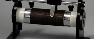
A conventional transformer circuit includes a low-frequency transformer with a primary and secondary winding. Pulse conversion also implies the presence of a transformer, but a high-frequency one.
Attention! High-frequency pulse transformers are smaller in size and cheaper, but their power is higher.
Pulse voltage converters (PVC) allow the use of three types of circuits:
- increasing;
- downward;
- inverter
IPNs have high efficiency and small dimensions. They include the following elements:
- power supply (power supply);
- key – switching element;
- energy storage device of inductive nature – inductor, coil;
- blocking diode;
- output voltage filter – high-capacity capacitor.
The filter is usually connected in parallel with the load.
Stabilizer on PT4115
PT4115 is a unified chip developed by PowTech specifically for building drivers for high-power LEDs, which can also be used in cars. A typical PT4115 connection circuit and the formula for calculating the output current are shown in the figure below.
You can understand why this happens, as well as get acquainted with a more detailed calculation and selection of the remaining elements of the circuit here. The microcircuit gained fame due to its versatility and a minimal set of parts in the harness. To light an LED with a power from 1 to 10 W, the car enthusiast only needs to calculate the resistor and select the inductance from the standard list.
The PT4115 has a DIM input that greatly expands its capabilities. In the simplest version, when you just need to light the LED at a given brightness, it is not used. But if it is necessary to adjust the brightness of the LED, then either the signal from the output of the frequency converter or the voltage from the output of the potentiometer is supplied to the DIM input. There are options for setting a specific potential at the DIM pin using a MOSFET. In this case, when power is applied, the LED glows at full brightness, and when the MOSFET starts up, the LED dims the brightness by half.
The disadvantages of an LED driver for cars based on PT4115 include the difficulty of selecting the current-setting resistor Rs due to its very low resistance. The service life of the LED directly depends on the accuracy of its rating.
Both microcircuits discussed have proven themselves to be excellent in constructing drivers for LEDs in a car with your own hands. LM317 is a long-known, proven linear stabilizer, the reliability of which is beyond doubt. A driver based on it is suitable for organizing interior and dashboard lighting, turns and other elements of LED tuning in a car.
PT4115 is a newer integrated stabilizer with a powerful MOSFET transistor at the output, high efficiency and dimming capability.
Principle of operation
Voltage stabilizer 12 volts
A switching voltage regulator uses the principle of comparing the reference voltage with the output voltage. The circuit allows you to adjust the duration of the key opening. The input voltage from the power source (PS) is passed by the switch according to the control signal of specified parts (pulses), taking into account that the average potential (lowered or increased) was stable.
IC block diagram
Comparison with linear stabilizer
Transistor voltage stabilizer
To compare the two conversion principles, you need to remember that linear stabilizers (LS) are usually a voltage divider. Its unstable potential is supplied to the input of the divider, and the stable potential is removed from the second (lower) arm. The principle of stabilization is to constantly change the resistance of the upper arm of the circuit so that on the lower arm it remains stable.
For your information. When the Uin/Uout ratio is high, the efficiency of the linear stabilizer is very low. This is due to energy losses on the regulating resistor. It heats up, which is why some of the input power is lost.
Such assemblies have their advantages, namely: simplicity of the circuit, a minimum of elements and the absence of interference. Compared to linear ones, switching stabilizers (IS) are more complex, but they work more stable when the circuit is properly selected.
Self-oscillations may occur in the IC, which lead to partial inoperability or complete failure of the converter. This occurs when the source impedance Uin exceeds the value of the IC impedance, then as Uin decreases, the input current increases.
Types of current stabilizers
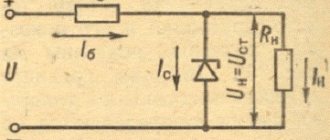
The current stabilizer sets a given current through the LED, regardless of the voltage applied to the circuit. When the voltage on the circuit increases above the threshold level, the current reaches the set value and does not change further. With a further increase in the total voltage, the voltage on the LED stops changing, and the voltage on the current stabilizer increases.
Since the voltage on the LED is determined by its parameters and is generally unchanged, the current stabilizer can also be called an LED power stabilizer. In the simplest case, the active power (heat) generated by the device is distributed between the LED and the stabilizer in proportion to the voltage across them. Such a stabilizer is called linear. There are also more economical devices - current stabilizers based on a pulse converter (key converter or converter). They are called pulsed because they pump power inside themselves in portions - pulses, as needed by the consumer. A proper pulse converter consumes power continuously, internally transmits it in pulses from the input circuit to the output circuit, and delivers power to the load again continuously.
Functional diagrams by type of control circuit
Parametric voltage stabilizer
Based on the type of control circuit, several operating circuits can be distinguished, including:
- Schmitt trigger;
- PWM – pulse width modulation;
- PFM – pulse frequency modulation.
Important! Switching regulators are self-regulating devices that rely on a reference voltage to serve as a reference for the regulation circuit.
Block diagrams of IPN with Schmitt trigger and PWM
With Schmitt trigger
With this stabilization circuit design, the upper and lower trigger thresholds are compared with Uin. For this purpose, a comparator is used - a comparison device. The key opens at the moment when the output voltage equals the trigger voltage (Umax). The energy accumulated during this time is supplied to the load, and Uout then decreases. As soon as its value reaches Umin (lower threshold), the trigger switches, closing the switch.
This method is called stabilization with two-position adjustment or relay. Circuits with a Schmitt trigger have voltages at the output of the device with a ripple value determined by the difference in response thresholds. This pulsation is practically impossible to eliminate.
In an IC with a Schmitt trigger, frequency conversion depends on Uin and In (load current) and is variable.
With pulse width modulation
At the output of such circuits, Uav (average) is obtained, which is influenced by the duty cycle of the pulses and Uin. An operational amplifier (op-amp) is a circuit for comparing Uout and Uop (reference) by subtraction and subsequent amplification. The result goes to the modulator, which adjusts its parameters depending on this result.
The modulator changes (increasingly) the ratio of the time at which the key is open to the period of the generator clock pulse if Uout < Uop.
The circuit achieves such a switch control that the difference between Uout and Uop is minimized when Uin or the current through the load (In) changes.
Attention! In ICs with PWM, frequency conversion does not depend on Uin and In.
With pulse frequency modulation
Such assemblies differ in that the duty cycle of the pulses (frequency) directly depends on a decrease in Uin or an increase in In. In this case, the duration of the pulse unlocking the key is unchanged. The pulse frequency is subordinated to the signal of the difference between Uout and Uop. A monostable multivibrator with a controlled trigger frequency can easily cope with sending commands to the switch.
Monostable transistor multivibrator
Purpose of drivers for LEDs
The brightness of an LED lamp depends on 2 parameters: the current passing through it and the identity of the characteristics of the semiconductors, since any discrepancy will damage the parts. But modern production is not able to provide completely identical crystal parameters.
It converts electric current:
- sets its amplitude;
- straightens - makes it permanent;
- supplies the same current to all elements (slightly less than the maximum level) and prevents their breakdown.
Key Features
The main difference between the driver is that at the input voltage for which it is designed (for example, 140-240 V), it sets the specified current level on the LEDs. In this case, the potential at the output of the device can be any.
It has 3 main characteristics:
- Rated current. It should not exceed the rated value of the LED, otherwise the diodes will burn out or glow dimly.
- Output voltage. Depends on the type of connection of semiconductors and their number. It is equal to the product of the potential drop of 1 element by their number and can vary within wide limits.
- Power. The entire operation of the device depends on the correct calculation of this characteristic. To do this, sum up the powers of all elements and add 20-25% (overload reserve).
For an LED lamp with 10 elements of 0.5 W each, this parameter will be equal to 5W. Taking into account overload, you should choose a 6-7 W driver.
But the last 2 parameters (power consumption and output voltage) directly depend on the emission spectrum of the LED. For example, XP-E elements (red) at 1.9-2.5 V consume 0.75 W, and green ones consume 1.25 W with a power supply of 3.3-3.9 V. It turns out that the driver is 10 W capable of powering 7 diodes of one color or 12 of another.
Power theory for LED lamps from 220 V
An ice lamp, ceiling strip or backlight on a modern TV is a combination of several powerful small LEDs placed in the space in the right way.
If each of them is capable of passing a current of 1 A at a voltage of 3.3 V, then they cannot be included in the lighting network - they will immediately burn out. You can use a resistor divider, but they will dissipate a lot of power. Therefore, the efficiency of the lamp will be small.
Drivers are used to reduce voltage and convert current into direct current. Inside these devices there may be various current stabilizers, capacitive-resistive dividers, etc.
The circuit may include transistors, microcircuits, capacitors, etc. Such converters change the voltage and provide the required amount of current to each element.
Basic circuits of the power section
Depending on the purpose of the IS, three basic models of its construction can be distinguished:
- downward;
- increasing;
- inverting.
Regardless of the design and purpose of the IC, devices used as a key can be:
- thyristor;
- transistor (bipolar or field effect).
The main task of such an element is to open or close upon a command received by the control electrode.
Buck Converter
Typically, it is necessary to reduce the voltage more often, which is why such ICs are more in demand.
The simplest step-down IC circuit
For the step-down voltage stabilizer shown in the diagram, the switch on field-effect transistor VT1 will open when control voltage is applied to it. The current from the positive terminal will flow to the load through the smoothing choke L1. The diode VD1 connected in parallel to the circuit does not currently pass current. After opening the key, the current circuit is as follows: inductor L1 – load – common wire – diode VD1 – inductor L1. In this case, the current passing through the inductor will not stop instantly, but will gradually decrease.
Important! For chokes with high inductance, it does not become equal to zero until the next opening of the key. Installation of such elements is impractical due to increased size and cost.
At this time, capacitor C1 will be discharged to the load and maintain U out. Capacitance C, together with inductance L, forms a filter that reduces the ripple range.
Boost converter
Unlike lowering Uin, this type of circuit is used to power load circuits that require a voltage higher than that of the source to operate.
Boosting IP
The circuit components are the same, but included differently. When the transistor is open, the diode is closed, and the current in the inductor increases linearly. When the key is locked, the current begins to move along the circuit: positive terminal - inductor L1 - diode VD1 - load - negative terminal. Capacitor C1 will be charged at this time. It will maintain current on the load while it discharges to it the next time the key is opened.
Inverting converter
Such an assembly also does not have galvanic isolation between the input and output stages. It has a completely different connection of the inductor, capacitor and load. They are located in parallel.
Inverting IC
When the VT1 key is open, current flows through the circuit: positive terminal - transistor - inductor - negative terminal. The choke stores energy with the assistance of a magnetic field. When the transistor closes, the current flow path changes: inductor - capacitor C1 - diode VD1 - inductor. The energy of the inductor and the energy of the capacitor will be completely transferred to the load. The amplitude of the ripple depends entirely on the capacitance C1. At this moment, the voltage across the load does not change, despite the fact that the current through C1 drops almost to zero.
By the way. The output voltage of inverting ICs may differ from the voltage of the power supply, either up or down.
Menu
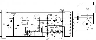
Let's consider the circuit design and functionality of step-down pulse stabilizer microcircuits in their development.
The circuit of a pulse step-down voltage stabilizer is shown in Fig. 1. A detailed consideration of the stabilizer operation process can be found in specialized literature, for example in [1]. Let us only recall that without taking into account losses in the circuit elements, the output voltage is determined as follows:
where ton is the time the key is open, T is the pulse repetition period.
This allows, by changing the ratio of the time the switch is open and the pulse repetition period, to regulate the output voltage, and in the presence of a negative feedback circuit, to stabilize it.
Both bipolar and field-effect transistors are used as a VT switch, and a field-effect transistor is used instead of a VD diode in stabilizers with synchronous rectification.
The first implementation of a pulse step-down voltage stabilizer was a relay (hysteresis) pulse converter, which has a very simple circuit design.
If for most pulse converter circuits the presence of output voltage pulsations is almost inevitable, then for a relay converter the presence of ripples reduced to the feedback input, equal to the comparator hysteresis voltage, is a prerequisite for normal operation.
A simplified diagram of a relay converter is shown in Fig. 2. A characteristic and “unpleasant” feature of the circuit is the dependence of the conversion frequency on the parameters of the circuit elements and the operating mode of the stabilizer:
As follows from the above formula, the frequency depends on the input and output voltages, the equivalent series resistance of the output capacitor, the inductance of the inductor and the hysteresis voltage of the comparator. Changing the frequency within a wide range does not allow optimizing the dimensions of the inductor and output capacitor, and complicates the fight against radiated interference.
In Fig. Figure 3 shows a practical circuit of a relay converter, which includes an LM317 linear stabilizer chip. This solution - the use of inexpensive integrated circuits of linear stabilizers - was used at first in the absence of specialized switching stabilizer microcircuits.
Although at present the relay control method in its pure form is practically not used, its undoubted advantages, such as the short transition time and the absence of frequency response correction elements in the feedback circuit, force developers to look for new design solutions using it.
In Fig. Figure 4 shows a stabilizer circuit with the popular MC34063 microcircuit from Motorola. The frequency of natural oscillations of the generator is set by the capacitance of capacitor C2, the frequency of forced oscillations of the generator is higher and depends on the maximum switch current set by the current limiting resistor R1. Since the rate of rise of current in the inductance depends on the difference between the input and output voltages, the conversion frequency increases with increasing input voltage. When the voltage at feedback pin 5 becomes equal to the reference voltage, the comparator, through a logic element and a trigger, prohibits control of the output switch for one or more periods of the generator frequency. Thus, the stabilizer operates in the mode of generating pulse packets. The efficiency of the stabilizer does not exceed 70%, the main losses are due to the large voltage drop across the composite switch transistor and the current limiting resistor.
An updated version of the MC34063 - the NCP3063 chip from ON Semiconductor - has a more advanced circuit for limiting the maximum switch current, operating only in transient and emergency modes, and is supplemented with temperature protection.
Temperature protection, provided in many modern microcircuits intended for power electronics, switches powerful output stages to the off state when the crystal temperature slightly exceeds the maximum permissible. This significantly increases the operational reliability of the equipment.
In the ADP1111 chip (the circuit in which it is included is shown in Fig. 5), the generator frequency is fixed and equal to 72 kHz. Regulation of the output voltage is ensured by stopping the generator when the output voltage reaches the nominal value, that is, as in the previous circuit, the stabilizer operates in the mode of generating pulse packets. When the generator is stopped, the microcircuit's own consumption is only 300 μA, which makes the circuit very efficient. The additional amplifier is intended for constructing circuits for a voltage detector, an error amplifier, or an additional linear stabilizer. Versions of the microcircuit with a fixed output voltage have a built-in divider in the negative feedback circuit. The microcircuit has built-in switch current protection with the ability to reduce the protection response current using an external resistor RLIM, which ensures adjustment of the maximum output current of the stabilizer.
Limiting the maximum output current of the stabilizer by setting the maximum switch current by the user is allowed by a limited range of microcircuits. If necessary, you can use a technical solution using a microcircuit - a current meter, proposed in [2].
Using modern capacitors at the stabilizer output, ripples at the generator operating frequency can be made very small. Ripple caused by the termination of the output switch cannot be less than the comparator hysteresis, the typical value of which is 2 mV for the MC34063 and 8 mV for the ADP1111, multiplied by the ratio of the output voltage to the reference voltage.
A modified relay control method is used in one of the latest families from National Semiconductor - LM5007, LM5008, LM5010. The circuit of the switching stabilizer on LM5007 is shown in Fig. 6. In this circuit, the time the switch is open, inversely proportional to the input voltage, is set by resistor R1. When the output current is more than 50 mA, the stabilizer operates in a mode with continuous inductor current and a constant switching frequency, determined by the formula:
The conversion frequency does not depend on the input voltage and load.
At low output current, the converter operates in intermittent inductor current mode and at lower frequencies, which minimizes losses. The operating frequency in this mode is determined by the expression:
To ensure normal operation of the stabilizer with modern capacitors, which, as a rule, have low values of equivalent series resistance, resistor R6 is connected in series with capacitor C2. The output voltage ripple is high, since for the stabilizer to operate, the ripple voltage at the feedback pin is recommended within 25-50 mV. If a lower level of output voltage ripple is required, the load can be connected in parallel with capacitor C2, or an additional LC filter that is not covered by the negative feedback circuit will need to be turned on at the output of the stabilizer.
A “charge pump” circuit is used to power the gate of the n-channel MOSFET. Capacitor C4, connected to the BST pin, is charged through the built-in diode during the closed state of the key. At the stage of the open state of the switch, the voltage on the capacitor is summed with the input voltage, which provides a higher voltage at the gate of the transistor than at its drain.
As can be seen from the functional diagram of LM5007, the microcircuit is significantly more complex than those discussed above, and includes components that increase operational reliability. Input undervoltage protection prevents the output transistor from turning on when the input voltage is less than 6.3 V, when the control circuit is no longer capable of adequate action. This prevents the microcircuit from failing in an emergency. Output overvoltage protection immediately locks the output switch if the FB pin voltage exceeds the 2.875 V threshold due to a sudden increase in input voltage or load disconnection. The current limiting circuit sets the maximum switch current at 0.725 A and, in addition, regulates the open time of the switch, set by resistor R2, during turn-on and overload. When the SD/Ron pin is shorted to ground, the stabilizer can be turned off, and the current consumed from the power source is equal to the sum of the microcircuit's own current consumption of 100 μA and the current through resistor R1.
Higher quality conversion characteristics are provided by the PWM control technique used in the vast majority of step-down stabilizer microcircuits. The conversion frequency is usually constant, which makes it possible to optimize the parameters of the inductor and capacitor of the output filter and simplifies the task of filtering noise at the conversion frequency. The amount of output voltage ripple is significantly less than in relay stabilizers, but the response to sudden changes in load or input voltage is noticeably worse. To ensure stability, frequency correction in the negative feedback circuit is required.
Rice. 7 explains the principle of voltage-controlled PWM control. The output voltage or part of it is fed to the input of an error amplifier, the other input of which is connected to the reference voltage Vref. The amplified voltage difference is supplied to the input of a PWM comparator, the other input of which receives a sawtooth voltage with the frequency of the master oscillator. Comparing these two voltages, the comparator modulates the duration of the pulses that control the switch S. The frequency correction circuits are conventionally shown in the form of complex resistances Z1 and Z2.
A practical circuit of a PWM stabilizer using the TPS5430 chip from the Swift™ series from Texas Instruments is shown in Fig. 8. Due to the high frequency of the master oscillator - 500 kHz, the correction capacitors have small values, and the frequency correction elements are integrated into the microcircuit. The most complex type 3 frequency correction used was used, more details about which can be found in the publication [3], dedicated to the frequency correction of switching stabilizers. In Fig. 9 the circuit is shown with a ceramic output capacitor C3. When using electrolytic capacitors, correction elements C4, C6, C7, R3 are not needed; internal correction is sufficient.
The microcircuit includes a circuit for generating an increased supply voltage for the n-channel MOSFET driver, protection against low input voltage, protection against high output voltage, and thermal protection. The resistance of the open MOS transistor channel is used as a current sensor in the circuit for limiting the maximum current of the switch. When the drain current reaches a threshold value, the switch turns off until the end of the current clock period. In the event of a serious overload, for example, in the event of a short circuit at the output, the HICCUP signal short-circuits the reference voltage source to ground for 10–20 ms, followed by a soft start of the stabilizer and repeating the cycle until the overload is eliminated. The soft start circuit provides a linear increase in the voltage at the input of the error amplifier from zero to the reference voltage in 8 ms. When the ENA pin is shorted to ground, the stabilizer can be turned off, while the current consumption does not exceed 50 μA.
The change in ramp voltage amplitude is inversely proportional to the change in input voltage, which provides better stability and shorter response time to disturbance in the form of a change in input voltage.
In Fig. Figure 9 shows the stabilizer circuit on the NCV8842 chip from ON Semiconductor, which uses patented V² control technology.
Conventional, relatively slow, negative feedback through the error amplifier provides high accuracy in maintaining the output voltage in static mode. Frequency correction is provided by a low-pass filter formed by a large output impedance of the error amplifier, about 8 MΩ, and an external capacitor C4. The absence of an amplifier in the fast negative feedback circuit provides it with a wide bandwidth, which significantly improves the dynamic characteristics of the stabilizer.
The driver of the bipolar transistor switch is powered by an increased voltage, which allows the transistor to be maintained in saturation when the output switch is open. The key transistor is two-emitter; a resistor is connected to the second emitter of a smaller area - a current sensor.
The conversion frequency is fixed and equal to 170 kHz. Using external clock pulses applied to the SYNC pin, you can increase the conversion frequency to 355 kHz and synchronize the operation of several chips in the device. In this case, it is possible to organize the operation of two or more stabilizers with a phase shift to reduce the pulse current through the capacitor at the input of the stabilizer, which reduces the requirements for the capacitor and simplifies its selection.
The peculiarity of the microcircuit is to reduce the clock frequency of the generator to a quarter of the nominal value, while simultaneously reducing the current protection threshold to 40% of the nominal value, until the feedback voltage reaches the operating threshold in the frequency feedback circuit, which ensures a reduction in power dissipation by microcircuit and external components during switching on and during overloads.
PWM stabilizers with current control have more advanced dynamic characteristics compared to voltage-controlled stabilizers, which also have better stability. In addition to negative voltage feedback, their circuit includes a high-speed current feedback circuit, as shown in Fig. 10. The current feedback signal comes from the key current sensor, is allocated to the current measuring resistor RI and is summed with the voltage feedback signal.
A practical circuit of a current-controlled stabilizer on the SC4518H chip from Semtech is shown in Fig. 11. Conversion frequency is fixed - 600 kHz, in external synchronization mode - up to 1.2 MHz.
The current feedback signal is taken from the current sensor, a 0.04 Ohm resistor connected to the collector of the key transistor. The voltage drop across the current-measuring resistor is increased by the current amplifier, summed with a sawtooth voltage generated by the master oscillator, and fed to the input of the PWM comparator, becoming the reference signal for the voltage feedback signal coming from the output of the error amplifier. The signal from the current amplifier also enters the current limiting circuit during overload.
The stability of the stabilizer is ensured by external correction elements R3, C4, C5. The ramp voltage slope correction circuit eliminates the possibility of self-excitation of the stabilizer at subharmonics at a duty cycle of more than 50%, which current feedback stabilizers are prone to. More details about the essence of the phenomenon and how to eliminate it can be found in [4].
The maximum switch current is limited by the overcurrent protection circuit at 2 A. In case of prolonged overload or short circuit at the output, periodic soft start attempts are made
The LM25005 chip uses so-called “quasi-current” control. As can be seen from the functional diagram of LM25005 in Fig. 12, the current feedback signal is taken from a resistor connected in series with diode VD1. The chip has a wide input voltage range of 7-42 V and is optimized for high input voltage applications. With a large ratio of the input voltage to the output voltage, the duty cycle becomes very small, and distortions of the current shape of the switch on the current sensor, inevitable due to the presence of parasitic elements in the circuit, worsen the control characteristics. On the contrary, the duration of the current pulse through the diode in this case is a significant part of the period, and distortions at the pulse fronts have a lesser effect. The sample-and-hold circuit generates a constant voltage at the output, proportional to the amplitude of the current through the current-measuring resistor, and the sawtooth component is restored in the adder. The current charging capacitor C3, on which a sawtooth signal is formed, depends on the input and output voltages, and to eliminate oscillations at subharmonics, a constant component is present in the charging current, correcting the slope of the “saw”.
Unique switch current control circuit and overload protection. When operating correctly, the recovered signal is proportional to the key current and, if its amplitude exceeds the threshold of the current limit comparator (1.75 V), the key is immediately locked. If the inductor inductance is low or the input voltage is high, the current through the switch may exceed the permissible value due to propagation delay in the comparator. When such an overload occurs, the sample/hold circuit detects excessive current during the open state of the switch, the switch is locked, and several pulses are passed until the voltage at the adder output is less than 1.75 V.
Another feature of the microcircuit is the guaranteed charging of the boost capacitor C7 at low load through a switch connected to the PRE pin, which opens for 250 ns in each cycle at the stage of the closed state of the output switch.
The frequency of the master oscillator is set by resistor R3 in the range of 50–500 kHz; by applying synchronizing pulses to the SYNC pin, the generator can be made to operate at a frequency higher than the natural oscillation frequency.
A soft start is ensured by charging capacitor C4, connected to the SS pin, to the reference voltage, and ultimately to the non-inverting input of the error amplifier, at a constant current of 10 μA. By changing the capacitance of the capacitor, you can change the delay time for the stabilizer to return to nominal mode.
In Fig. Figure 13 shows a circuit of a stabilizer with synchronous rectification and control by the average inductor current using the Maxim MAX5061 controller chip. Control based on the average current of the inductor is free from problems associated with amplification of short current pulses, masking of interference on their fronts, and signal propagation delays inherent in the control method based on the maximum current of the switch.
Since the stabilizer is designed for high output current, the powerful output transistors are external. Energy is transferred to the load and stored in the inductance when the high-side transistor is turned on. At this time, the low-side transistor is closed. And, conversely, when the lower-side transistor is open, the upper-side transistor is closed, and the energy stored in the inductance is relayed to the load. Synchronous rectification circuits are especially effective at low output voltages. The losses in the low-side transistor are many times less than in the diode it replaces.
The current feedback circuit consists of a current sense resistor R1 in series with the inductor, a precision differential current amplifier, a current error amplifier, and a PWM comparator. The output voltage of the current error amplifier is the amplified difference between the output voltage of the voltage error amplifier and the current amplifier. This ensures that the inductor current is adjusted in accordance with the output voltage. The frequency response of the current error amplifier rolls off at high frequencies, which reduces the influence of noise and interference in the signal from the current sensor. External frequency response correction elements, which require careful calculation, are connected to the CLP pin connected to the output of the current error amplifier.
A soft start is organized by applying a linearly increasing voltage of 0–0.7 V from a 5-bit DAC to the third (non-inverting) input of the voltage error amplifier. As long as the voltage at the DAC output is less than the reference voltage of 0.6 V, the circuit operates under the control of the DAC, then switches to operating mode with the reference voltage.
The conversion frequency is set from 125 kHz to 1.5 MHz by an external RT resistor connected to the RT/SYNC/EN multifunction pin. With the corresponding signals supplied to this pin, the stabilizer can be synchronized from an external generator or turned off.
With a maximum permissible input voltage of 27 V, the output voltage cannot exceed 5.5 V, the maximum input common-mode voltage of the current amplifier, limited by the voltage of the built-in stabilizer that powers all components of the microcircuit.
Another example of a stabilizer with synchronous rectification using the MIC2285 microcircuit from Micrel, operating at a conversion frequency of 8 MHz, is shown in Fig. 14. The efficiency of a specific stabilizer circuit reaches 90%. The upper-side transistor is p-channel, so there is no voltage booster circuit to power its driver.
With an output current not exceeding 60 mA, when a high logic level is applied to the LOWQ pin, the circuit can be switched to LDO stabilizer mode, which will reduce the circuit's own consumption and reduce the noise level in the output voltage.
The NCP1500 chip has similar capabilities, which works as a step-down stabilizer with synchronous rectification in the presence of synchronization pulses, automatically switching to skip-pulse mode at low load, and in the absence of synchronization pulses, the circuit switches to linear LDO stabilizer mode.
Pulse converter microcircuits, intended for use in computers and portable equipment, have complex functional circuits, including several channels of pulse and linear stabilizers with output voltage controlled by digital inputs, a certain order of their activation and other additional functions. An example of such a chip is the MPC18730 from Freescale Semiconductor, controlled by a microcontroller via a three-wire interface and including two buck switching regulators with synchronous rectification, one boost switching converter and three linear LDO regulators.
Chip manufacturers strive to integrate the components and functions of the stabilizer into the chip as much as possible, but not everything is possible. The range of microcircuits with a built-in diode is small, the technology of high-speed diodes does not combine well with the technology of integrated circuits, and the area occupied by the diode on the chip is too large. These include one of the first switching stabilizer chips from Motorola - μA78S40, the slow built-in diode of which the manufacturer himself recommends replacing with an external high-speed one, and LT1572 from Linear Technology with a built-in Schottky diode (1 A, 20 V). The MIC33050 microcircuit from Micrel, a 0.5-A stabilizer with an integrated choke, operating at a frequency of 4 MHz, also remains exotic.
The selection of a suitable microcircuit is facilitated by interactive tables posted on manufacturers' websites, which allow sorting by selected parameters. Free programs such as Webench from National Semiconductor, Swift Designer Tool and SwitcherPro™ from Texas Instruments, LTSpice/SwitcherCAD III from Linear Technology, contain a large number of examples of converter circuits of various configurations, allow you to calculate the parameters of external components, simulate a stabilizer circuit and observe signals in various circuits of the circuit.
Literature
- Meleshin V.I. Transistor converter technology. M.: Tekhnosphere, 2005.
- Maxim/Dallas. Application Note 478. Current-Limit Circuit for Buck Regulator.
- A General Approach for Optimizing Dynamic Response for Buck Converter. Application Note AN8143/D, ON Semiconductor.
- Modeling, Analysis and Compensating of the Current Mode Controller. Application Note U-97, Unitrode. slua101.pdf. Texas Instruments.
Effect of diode on efficiency
A diode connected to an electrical circuit causes a voltage drop of 0.4 to 0.7 V. At a current of several amperes and a low Uout, a loss of power occurs on the element, which leads to a decrease in efficiency. An alternative option is used - replacing the diode with a field-effect transistor. Select one so that in the open state the voltage drop across it is minimal.
Attention! Instead of a diode, you can put another switch in the circuits, which will work in antiphase with the main one.
Features of use
Switching stabilizers can be used as drivers for LEDs and LED lamps. In addition, they are used in various devices, such as:
- power supplies for LCD television receivers;
- navigation equipment;
- power supplies for computers and digital system devices.
Switching stabilizers are used for chargers and converting alternating current into direct electricity.
Pulse noise filtering
Strong interference emitted by a pulse voltage stabilizer (VST) at the moment of switching the switch (current and voltage surges) must be suppressed. This requires applying filters and placing them at the input and output.
Input impedance
For ISNs operating under load, as Uin increases, the input current (Iin) decreases. This means its input impedance is negative differential. When connecting the ISN to sources with high internal resistance, unstable operation is possible.
Use in AC networks
To connect to an alternating current source, a rectifier and filter are installed in front of the ISN. This is an area where there is a danger of electric shock to a person. Elements included in this area must be protected from touch or marked with a marker (graphic and color warning).
Benefits of OS regulation
IC voltage regulation feedback is an important option for switching regulators. It allows you to maintain a stable voltage at the output of the device, sensitively monitoring surges in voltage and current. The ISN uses broadband feedback (the wider the frequency interval, the lower the ripple level as a result).
The availability of components for constructing ISN on the radio components market makes it possible to assemble any of the pulse stabilizer circuits with your own hands. The use of ready-made stabilizers on integrated circuits (ICs) and switches on field-effect transistors makes the device as compact as possible.
Advantages and disadvantages
Like all devices, a modular switching stabilizer is not ideal. Therefore, it has its own pros and cons. Let's look at the main advantages:
- Easily achieve alignment.
- Smooth connection.
- Compact sizes.
- Output voltage stability.
- Wide stabilization interval.
- Increased efficiency.
Disadvantages of the device:
- Complex design.
- There are many specific components that reduce the reliability of the device.
- The need to use power compensating devices.
- Difficulty of repair work.
- Formation of a large amount of frequency interference.