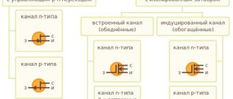
Now let's talk about field effect transistors. What can you assume from their name alone? Firstly, since they are transistors, they can be used to somehow control the output current. Secondly, they are supposed to have three contacts. And thirdly, their operation is based on a pn junction. What will official sources tell us about this?
Field effect transistors
are active semiconductor devices, usually with three terminals, in which the output current is controlled by an electric field.
(electrono.ru)
The definition not only confirmed our assumptions, but also demonstrated a feature of field-effect transistors - the output current is controlled by changing the applied electric field, i.e. voltage. But for bipolar transistors, as we remember, the output current is controlled by the input base current.
Another fact about field-effect transistors can be learned by paying attention to their other name - unipolar
. This means that only one type of charge carrier (either electrons or holes) is involved in the process of current flow.
Before moving on to the story about the physics of the operation of unipolar transistors, I would like to remind you of the links where you can refresh your knowledge about the pn junction: one and two.
Expert opinion
Viktor Pavlovich Strebizh, lighting and electrical expert
Any questions ask me, I will help!
We connect the red probe to pin B and check the resistance with the black probe by touching terminals K and E, alternately, it should be minimal. If there is something you don’t understand, write to me!
How to measure the gain of a transistor with a multimeter
- Maximum drain current
at a fixed gate-source voltage. - The maximum drain-source voltage
, after which breakdown occurs. - Internal (output) resistance
. It represents the channel resistance for alternating current (gate-source voltage is constant). - Slope of the drain-gate characteristic
. The larger it is, the “sharper” the transistor’s response to changes in gate voltage. - Input impedance
. It is determined by the resistance of the reverse-biased pn junction and usually reaches several and tens of megohms (which distinguishes field-effect transistors from their bipolar “relatives”). And among the field-effect transistors themselves, the palm belongs to devices with an insulated gate. - Gain
is the ratio of the change in source-drain voltage to the change in gate-source voltage at a constant drain current.
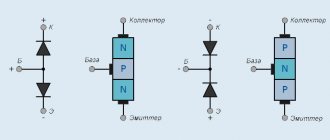
Field effect transistor with control pn junction
The following analogy can be drawn: a pn junction is a dam that blocks the flow of charge carriers from source to drain. By increasing or decreasing the reverse voltage on it, we open/close the gateways on it, regulating the “water supply” (output current).
Even with zero gate voltage, there is a reverse voltage between gate and drain equal to the source-drain voltage. This is why the pn junction has such a jagged shape, widening towards the drain region.
It goes without saying that it is possible to make a transistor with an n-type channel and a p-type gate. The essence of his work will not change.
Conventional graphic images of field-effect transistors are shown in the figure ( a
- with a p-type channel,
b
- with an n-type channel). The arrow here indicates the direction from the p-layer to the n-layer.
Static characteristics of a field-effect transistor with a control pn junction
Since in operating mode the gate current is usually small or even zero, we will not consider graphs of the input characteristics of field-effect transistors. Let's go straight to the weekend or stock. By the way, they are called static because a constant voltage is applied to the gate. Those. there is no need to take into account frequency moments, transients, etc.
Day off
(
drain
) is the dependence of the drain current on the source-drain voltage at a constant gate-source voltage.
The figure shows the graph on the left.
Three zones can be clearly distinguished on the graph. The first of them is the zone of sharp increase in drain current. This is the so-called "ohmic" region
. The source-drain channel behaves like a resistor whose resistance is controlled by the voltage at the transistor's gate.
The third zone of the chart is the breakout area
, whose name speaks for itself.
On the right side of the figure there is a graph of another important relationship - the drain-gate characteristic
. It shows how the drain current depends on the gate-source voltage when the voltage between the source and drain is constant. And it is its steepness that is one of the main parameters of a field-effect transistor.
Radio as a hobby
This stand allows you to determine such parameters of field-effect transistors with a pn junction as the initial drain current and cut-off voltage.
These parameters have to be determined quite often in amateur radio practice, when it becomes necessary to select a field-effect transistor according to these criteria.
The circuit diagram of this field-effect transistor test bench was entirely borrowed from the website of S. Belenetsky.
By clicking on the link above, you can get more detailed information about such parameters of field-effect transistors as the cut-off voltage Uots and the initial drain current Iin.
The stand is assembled according to a very simple scheme:
There’s not even anything to describe here.
As already indicated, this stand allows you to measure the cut-off voltage Uotc and the initial drain current Iin of field-effect transistors with a pn junction with both a p-channel (KP103) and an n-channel (KP303,307, BF245 and the like)
The stand is powered by a voltage of 9 V, and the power polarity indicated in the diagram is used when working with field-effect transistors with an n-channel (KP303,307, BF245 and the like). To work with transistors with a p-channel, the power polarity must be changed to REVERSE.
The stand is connected to a digital multimeter, which operates in DC voltage measurement mode.
After power is applied, the stand immediately measures the cutoff voltage Uots of the field-effect transistor installed in the socket. To measure the initial drain current Istart, simply press the button. In this case, the multimeter readings must be divided by 10, according to the formula indicated on the bench diagram.
The stand is assembled on a miniature printed circuit board measuring 25x35 mm. The appearance of the board indicating the elements is presented below:
The details used here are not scarce.
One subtle point - since the value of resistor R2 10 Ohm is included in the calculation formula for the initial drain current - we divide the readings by 10, it needs to be selected more precisely. I selected a 10.4 ohm resistor from my supplies.
As a socket for transistors, a socket for microcircuits was used, from which all excess was sawed off, leaving only five contacts.
Now let's talk about how to use this stand to determine the parameters of field-effect transistors.
Some real measurements:
We install the KP302B transistor in the socket. We connect a digital multimeter to the stand in the mode of measuring constant voltages at a limit of 20 V. We supply power and immediately read the cutoff voltage of the transistor in volts:
As you can see, the cutoff voltage of this instance of KP302B is 3.09 V.
Press the button and read the initial drain current:
The device shows 0.34. This is the voltage drop across resistor R2 (see diagram above).
The initial drain current is Ic=0.34 V/10 Ohm=0.034 A or 34 mA. In general, in order not to get confused, just mentally discard all the symbols to the left of the decimal point and we simply get 34 mA.
We measure the parameters of the KP103K transistor in a plastic case.
This transistor has a p-type channel. Therefore, we reverse the polarity of the power supply. I switched the multimeter to the measurement limit of 2000 mV, because reading readings at the 20 V limit is not very convenient for this type of transistor.
We turn on the power and see the cutoff voltage of 1314 mV, or 1.34 V.
Press the button and read the value of the initial drain current:
The tester showed 18 mV, divide by 10 (resistor R2) and get the initial drain current Ic = 1.8 mA.
The result was a simple, but quite useful device in many cases.
Conductor side printed circuit board:
A short video about the operation of this stand for measuring the parameters of field-effect transistors:
Restrictions
- When working with small-signal MOS transistors, you need to be extremely careful about static electricity so as not to kill them during such a test.
- MOS transistors operating in depletion mode (with a built-in channel) must be checked a little differently. This fact does not diminish the usefulness of this article, and here’s why: the probability that you will have such a device tends to an infinitesimal value. If you managed to get Depletion Mode MOSFET, do you really not need this article?
- If you are lucky enough to become the owner of a rare MIS device without a structural diode, then, accordingly, the structural diode check described below does not make sense.
- Perhaps the voltage on the multimeter probes is not enough to reliably open the transistor. Then you can take a 9-volt Krona battery with a resistor of at least 1KOhm in series and use this source to charge the gate.
1) The gate must be isolated from other terminals
- a) We connect the black “-” probe of the multimeter to the drain terminal (flange) or source terminal, and touch the gate terminal with the red “+” probe: the device shows an open circuit. We disconnect the probes in the reverse order: first from the gate, then from the source or drain. We make sure that nothing else touches the shutter output.
- b) Connect the red probe of the multimeter to the drain or source terminal, the black one to the gate: the device shows an open circuit. We first disconnect the probe from the shutter.
We discharge the gate capacity: take the transistor by the radiator mounting flange (drain terminal), if there is none, then first touch the drain or source terminal, then gently hug all three legs?
2) Check the structural diode.
To do this, we check the diode between the drain and the source for serviceability, just as we would check a regular silicon diode.
- a) In direct connection, the drop is the same as on a conventional silicon diode: the multimeter should show a voltage drop in the range of approximately 0.4 to 0.7 Volts.
- b) In reverse connection - the diode is locked.
3) We charge the gate capacity - the channel is open.
For n-channel MOS transistors (and the vast majority of them are):
In the case of a p-channel MOS transistor, the polarity is correspondingly reversed.
To do this, move the probe that just touched the shutter to the drain. The device should show a slight voltage drop, or even a short circuit; some devices beep happily. The charge flows from the gate of a working transistor extremely slowly - the channel must remain open for quite a long time.
4) Unload the shutter.
To do this, you can hold the flange or source terminal and touch the gate. You can do this with your fingers, you can use a wire, or you can repeat the procedure for charging the gate capacitance, but applying reverse voltage polarity.
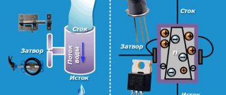
Field effect transistors. For dummies / Sudo Null IT News
If a source-drain voltage is applied at zero gate voltage, then current will flow through the channel between them. Why not through the crystal? Because one of the pn junctions will be closed.
Expert opinion
Viktor Pavlovich Strebizh, lighting and electrical expert
Any questions ask me, I will help!
However, there is another type of field-effect transistors with an insulated gate, a transistor with an induced inverse channel. If there is something you don’t understand, write to me!
How to check a field-effect transistor and read its main characteristics?
A simple universal device for measuring the parameters of JFET transistors with a built-in depletion type pn junction and enriched type MOSFET transistors.Recently, in amateur radio practice, devices built on field-effect transistors have become increasingly common. The reason for this is a number of useful qualities of field workers, such as: high input impedance, low noise level, low feed-through capacity, high temperature stability, etc., etc.
It would seem that this is happiness! But no - the main limitation when using any field-effect transistors is the spread of parameters. These parameters are individual for each specific instance and can vary significantly even for field-effect transistors of the same type from the same batch.
In different sources you can find all kinds of descriptions of PT parameter meters, but they are either complex or are the simplest testers for determining the initial drain current and cutoff voltage. The fairly simple device proposed for consideration allows you to measure the gate-source voltage at various (specified) drain currents. This makes it possible not only to immediately and accurately calculate the values of the resistors that set the operating mode of the cascade, but also to measure the current-voltage characteristics of the semiconductor, and when performing a couple of simple manipulations with a calculator, to calculate the steepness of the transfer characteristic. Objects for characterization can be either JFET transistors with a built-in pn junction or enriched MOSFET transistors. The parameters are read using an external voltmeter or multimeter (which is assumed to be available in every radio amateur) in the amount of one piece.
Fig. 1 Diagram of a device for measuring the characteristics of field-effect transistors
The measuring device presented in Fig. 1 is quite universal and is adapted to work with any field-effect transistors that require both positive and negative gate bias relative to the source. Taking into account the different conductivity of the PT, there are 4 of these types of semiconductors: n-type JFET, p-type JFET, n-type MOSFET and p-type MOSFET. In order to avoid arranging complex switching in the device, it was decided to use separate connection terminals for each type of field operator.
By and large, the circuit is a linear current stabilizer. The current sensor here is a pair of resistors R3, R5 (or R4, R6), the total resistance of which is calculated based on the formula R ≈ 0.6/Iload . As the current through the tested DC increases, the voltage drop across the sensor increases. When it reaches a value of 0.6V, transistor T2 begins to open, the voltage level at the PT gate drops, and the current decreases. In this way, Ic of the field-effect transistor is stabilized.
Since for normal operation of an n-channel JFET transistor the Uzi value must be in the negative region, the voltage at its source is fixed at 5.2V by means of a divider R1, R2 and an emitter follower T1. For an n-channel MOSFET transistor, the value of Uzi must be in the positive region, so its source is connected to ground.
For p-channel transistors, everything happens in a similar way, but with reverse polarity, for which the control circuit on transistors T3 and T4 is inverted relative to the power supply and ground.
As was said, the regulation of the drain current of the transistor under test is set by changing the resistance value of the current sensor. For ease of use of the device, the entire current adjustment range is divided into 2 subranges: 0.2…3mA and 2…35mA. In order to avoid the need to use an additional measuring device, potentiometers should be equipped with a scale and calibrated. Due to the fact that not every JFET transistor is capable of delivering a source current of 35 mA, it is better to perform calibration with some not very powerful MOSFET transistor, for example, an n-type MOSFET from the 2N7000 - 2N7002 series. Then everything is simple: 1. Install the field-effect transistor; 2. Temporarily connect an ammeter into the gap between its drain and the positive of the power source; 3. Place marks on the resistor scale corresponding to the instrument readings in both subranges of current change.
How to use the device?
1. The initial drain current of the field-effect transistor (only for JFETs) is the drain current at Uzi = 0. Turn the potentiometer until the voltmeter shows Uzi = 0V. The readings on the potentiometer scale will be the desired value of the initial drain current. In principle, this parameter has practical meaning only when calculating cascades with a common source, in which the source without a resistor is connected directly to ground (or the power bus for the p-type).
2. The cutoff voltage of a field-effect transistor is the voltage between the gate and source at which the drain current reaches a specified low value (10 μA ... 1 mA). The parameter for analog electronics is not very informative, but for switch MOSFETs it is set at a current of 250 µA and higher - therefore 200 µA produced by the device for measuring Uzi_ots is quite sufficient for practical use.
3. Voltage Uzi at a given drain current is the main parameter for calculating the amplifier stage on a field-effect transistor. There can be many criteria for choosing the value of the drain current, both in terms of achieving the required load capacity and other factors, such as: performance, noise characteristics, power consumption, stability of parameters, etc. Based on these criteria, the developer, as a rule, knows in advance at what current this or that stage on the DC will operate. Therefore, everything is very simple here: we set the required drain current with a potentiometer and measure it with a Uzi voltmeter. We discussed in detail how to further (taking into account the taken parameters) calculate the elements of cascades on field-effect transistors on the pages link to page 1 and link to page 2.
4. The slope of the transfer characteristic is an important parameter for calculating the gain of the cascade on a field-effect transistor. Since there is a fairly strong dependence of the slope on the initial drain current of the transistor, it must be measured in the immediate vicinity of the given drain current. Let's assume that the cascade will operate at a current Iс=2mA. Then voltage measurements Uzi can be carried out at currents of 1.5 and 2.5 mA, and the slope value can be calculated using the formula S = ΔIc/ΔUzi (mA/V).
Possible surprises
The vast majority of malfunctions of MIS transistors are in one way or another associated with breakdown of the gate insulator. This can manifest itself either as a completely measurable leak in the gate circuit, or in a constantly open or, on the contrary, closed state of the channel, without the slightest hint of breakdown of the gate itself.
The destruction of a crystal under overload is often accompanied by such fireworks that there is no need to measure anything there anymore.
What kind of lighting do you prefer?
Built-in Chandelier
Unfortunately, there are also hidden defects, degradation of the quality of the device, caused by a breakdown and which do not appear in any way in the tests described in this article. Recently I myself came across such a defect when working with small field workers (2n7002). What can I recommend here:
You May Also Like
Do-it-yourself surge protector for audio
Checking and selection of field-effect transistors
About resistors
How to check the field effect transistor KP303? (The electret microphone does not work
Maybe there is such a way? Otherwise, I can’t get the MKE-30 electret microphone to work. I can’t, that’s all. I tried everything. I have 5 of these KP303. but in these tests I may have killed them.
After all, they must be grounded when soldering, all four legs must be short-circuited. remove static tension from yourself. So I don’t know if they are alive. To press the microphone. He hesitated. It hasn't started for ages.
The element itself died. They have a limited lifespan. Although the electret should “live” for 30 years.
The drop itself?! And I thought that there were only two membranes, precisely located and distanced from each other. This is it. not a mechanism. to break.
But the head (capsule) is really old. And the size is much larger than the current ones that are sold. I assumed that this one had a better size and frequency.
And at the same time, I’ll ask. These transistors are not found in our radio components. They do not sell domestic parts. But not about that
I also wanted to buy the most economical blue LEDs. And there is only one type. It costs 8 rubles. The type of LED on the receipt is listed as GNL 5013BW (although the saleswoman dictated it to me as L 5013BC)
Is it economical? I need a circuit powered by the crown.
This is for purely capacitor ones. And for electret ones. //cxem.net/sprav/sprav96.php
PS. The smaller the distance between the membrane and the electrode, the smaller the diameter of the capsule. Technologically difficult task. For our drunks.
“Electret microphones operate on the same principle as condenser microphones, but the constant voltage in them is provided by the electret charge, which is applied in a thin layer to the membrane and retains this charge for a long time (over 30 years).”
Really. there is something temporary in them. Only about 30 years is a Jewish exaggeration. Ehh. it means it won't work. Are such heads produced now? With a fresh charge of electret? What would be bigger in diameter?
For music. Voice and sound recordings. I want frequencies, lenses.
For studio recordings, these expectations are naturally unreasonable. But. I want to listen. experiment.
And the power supply for such microphones is 48 volts. (and there is no battery compartment)
So. It seems to me that you should not ignore the quality of the capsule.
Although I. Interesting opinions on this. Maybe these capsules are potentially good. We just need to create conditions for the manifestation of this potential.
Expert opinion
Viktor Pavlovich Strebizh, lighting and electrical expert
Any questions ask me, I will help!
If you are lucky enough to become the owner of a rare MIS device without a structural diode, then, accordingly, the structural diode check described below does not make sense. If there is something you don’t understand, write to me!
How to test a field effect transistor?
If you now touch the bottom (G - gate) leg with the black probe, without releasing the red probe (Fig. 7), and return it to the substrate (D - drain), then the field-effect transistor will close and again show a resistance of about 500 Ohms (Fig. 8 ). This is true for most N-channel field devices in DPAK and D²PAK packages used on motherboards and video cards.
There is a diode in the drain-source circuit. By the way, its presence is due to production technology.
0.5V is the voltage drop across the internal Schottky diode. If you swap the probes, there should be a “break”.
The tester should show a “break” when testing gate-source and gate-drain, and the polarity of the probes does not matter.
But what’s interesting is that if you hold the black probe (“-“) at the source, and touch the gate with the red probe (“+”), the transistor will open. What can we be convinced of by checking again
Now let’s place the “+” probe on the drain and the black probe on the gate and check the drain-source. The tester will again show either a voltage drop across the diode or a “break”, i.e. the transistor has closed!
By the way, there is one more subtlety - if we open the transistor and measure the drain-source resistance, but not immediately, but after a while, then the tester will show a resistance other than zero. And the more time passes, the greater the resistance will be.
Why is this happening? And everything is very simple - the capacitance between the gate and drain is quite large (usually units of nanofarads) and when we open the MOSFET transistor, this capacitance is charged. And since the field-effect transistor is controlled by a field and not a current, the transistor will be open until the capacitor is discharged.
Description of work
To check, the first step is to connect each terminal of the transistor being tested to the corresponding terminals of the device: drain - to X3, gate X4, source - to X5.
After pressing the SA2 button, the audio frequency generator is activated. Oscillations in the generator arise as a result of the PIC, which is formed between the source and the gate. To enhance the PIC value, the circuit uses a matching step-up transformer T1, which has a transformation ratio of 3.57. The use of PIC is also explained by the fact that the field-effect transistor has a transmission coefficient of no more than one. Switch SA2 not only supplies power to the circuit, but also creates a primary current pulse to start the sound generator.
Certain types of field-effect transistors with a fairly high cut-off voltage begin to function only in this switching mode. But there are many types of transistors that do not require switching on using a pulse; after turning on the supply voltage, they begin to work immediately. Switch SA1 is necessary to switch the test mode depending on the type (channel type n or p) of the semiconductor.
The device uses a headset (dynamic head) BA1, which is used to listen to background sounds and check the operation of the transistor. A sound signal in the headphone appears when the field-effect transistor is working and is absent when it is faulty. This device is powered by 3 volts, it can be a stabilized power source or 2 AA batteries
Checking the functionality of the field-effect transistor
This type of semiconductor elements is also called mosfet and mosfet components. Figure 4 shows the graphic designation of n- and p-channel field switches in circuit diagrams.
To test these devices, we connect the probes to the multimeter in the same way as when testing bipolar semiconductors, and set the test type to “continuity”. Next, we proceed according to the following algorithm (for an n-channel element):
- We touch the black wire to the “c” pin, and the red wire to the “i” pin. The resistance on the built-in diode will be displayed, remember the reading.
- Now you need to “open” the transition (this will only be possible partially), for this we connect the probe with the red wire to terminal “z”.
- We repeat the measurement carried out in step 1, the reading will change downwards, which indicates a partial “opening” of the field worker.
- Now you need to “close” the component, for this purpose we connect the negative probe (black wire) to the “z” leg.
- We repeat steps 1, the original value will be displayed, therefore, “closing” has occurred, which indicates the serviceability of the component.
To test p-channel elements, the sequence of actions remains the same, with the exception of the polarity of the probes, it must be reversed.
Note that insulated gate bipolar elements (IGBT) are tested in the same way as described above. Figure 5 shows the SC12850 component in this class.
Fig 5. IGBT transistor SC12850
For testing, it is necessary to perform the same steps as for a field-effect semiconductor element, taking into account that the drain and source of the latter will correspond to the collector and emitter.
In some cases, the potential on the multimeter probes may not be enough (for example, to “open” a powerful power transistor); in such a situation, additional power will be needed (12 volts will be enough). It must be connected through a resistance of 1500-2000 Ohms.
Expert opinion
Viktor Pavlovich Strebizh, lighting and electrical expert
Any questions ask me, I will help!
For bipolar PNP conductivity devices, the open state will correspond to the connection of the negative black probe of the tester to the base terminal. If there is something you don’t understand, write to me!
The simplest probe for testing field-effect transistors (Field Mice.)
This article will present, in my opinion, the simplest, but no less effective circuit of Field Mice (field-effect transistors).
I think this circuit will rightfully take one of the leading positions on the Internet in terms of simplicity and reliability of assembly. Since there is simply nothing to shake or burn here... The number of parts is minimal. Moreover, the circuit is not critical to the ratings of the parts... And it can be assembled practically from rubbish, without losing its functionality... Many will say, why some kind of probe for transistors? If everything can be checked with a regular multimeter... And to some extent they will be right... To assemble a probe you need to at least have a soldering iron and a tester... To check the same diodes and resistors. Accordingly, if there is a tester, then a probe is not needed. Yes and no. Of course, you can check a field-effect transistor (field-effect mouse) for functionality with a tester (multimiter) ... But it seems to me that this is much more difficult to do than checking the same field-effect mouse with a probe ... I will not explain in this article how a field-effect mouse (field-effect transistor) works. So, for a specialist this has all been known for a long time and is not interesting, but for a beginner everything is complicated and complicated. So it was decided to do without boring explanations of the principle of operation of a field mouse (field-effect transistor).
So, the probe circuit, and how they can test a field-effect mouse (field-effect transistor) for survivability.
We assemble this circuit, even on a printed circuit board (the seal is attached at the end of the article). At least mounted installation. Resistor values can differ by about 25% in either direction.
Any button without locking.
The LED can be either bipolar, two-color, or even two back-to-back parallel. Or even just one. If you plan to test transistors of only one structure.. Only N channel type or only P channel type.
The diagram is assembled for field mice of the N channel type. When checking P channel type transistors, you will have to change the polarity of the circuit power supply. Therefore, another counter LED was added to the circuit, parallel to the first one.. In case you need to check a field mouse (field effect transistor) P channel type.
Many will probably immediately notice that the circuit does not have a power polarity switch.
This was done for several reasons.
1 No such suitable switch was available.
2 Just so as not to get confused in what position the switch should be when checking the corresponding transistor. I get N channel transistors more often than P channel ones. Therefore, if necessary, it is not difficult for me to simply swap the wiring. To test P channel field mice (field effect transistors).
3 Just to simplify and reduce the cost of the scheme.
How does the scheme work? How to test field mice for survivability?
We assemble the circuit and connect the transistor (field mouse) to the corresponding terminals of the circuit (drain, source, gate).
Without pressing anything, connect the power. If the LED doesn't light up, it's already good.
Go ahead. We press the button. The LED should light up. Which indicates the integrity of the field-effect transistor (which means the field mouse is alive and well).
If, when the transistor is correctly connected to the probe, power is supplied and the button is NOT pressed, the LED lights up... This means the transistor is broken.
Accordingly, if the button is pressed, the LED does NOT light up. This means the transistor is broken.
That's the whole trick. Everything is brilliantly simple. Good luck.
P/S. Why in the article do I call a field-effect transistor a field mouse? Everything is very simple. Have you ever seen transistors in a field? Well... Simple. Do they live there or grow there? I think no. But there are field mice... And here they are more appropriate than field-effect transistors.
And why are you surprised by the comparison of a field-effect transistor with a field-effect mouse? After all, there is, for example, the site radiokot or radioskot. And many other sites with similar names.. Which have nothing to do directly with living creatures... So.
I also think that it is quite possible to call a bipolar transistor, for example, a polar polar bear...
And I also want to express my deep gratitude to the author of this probe circuit, V. Goncharuk.
Share on social media networks
RќСЂР°РІРёС‚СЃСЏ
Transistors and checking them with a multimeter; how to check a transistor with a tester without desoldering
- The multimeter must be switched to diode test mode. It is marked on the panel with a schematic diagram of a diode.
- Two probes are attached to the device: black and red. There are three slots on the front panel. Black is set to the bottom, red to the middle. The first of them corresponds to the negative pole, the second to the positive pole.
- It is necessary to determine on the field-effect transistor being tested which outputs correspond to the source, gate and drain.
- Some models additionally have an internal diode that protects the part from overload. First you need to check how it works. To do this, the red wire is connected to the source, and the black wire to the drain.
MEASUREMENT OF FIELD TRANSISTOR PARAMETERS
Information about some parameters of a field-effect transistor can be obtained from the family of static current-voltage characteristics. The technique for measuring these characteristics does not differ from the similar technique for vacuum lamps. The simplest method is to take characteristics point by point. Since the circuit with a common source is typical, when taking current-voltage characteristics, the source is usually grounded, and adjustable voltage sources of the appropriate polarity and measuring instruments are connected to the drain and gate (Fig. 9).
Rice. 9. Scheme for reading the current-voltage characteristics of the PT.
The complete family of output current-voltage characteristics Iс=f(Uс,п) at Uз.и=const can also be obtained using a curve tracer. In this case, a sawtooth sweep voltage must be applied to the drain of the field-effect transistor, and a step voltage must be applied to the gate.
The drain saturation current Ic0 and the cutoff voltage Uots are usually measured at a drain voltage of 10 V and a gate voltage Uz.i=0. These parameters characterize at the same time the position of the inflection point of the characteristic. It was previously shown that
Ic=Ic0(1-Us.i/Uots)2
From this formula it is clear that the parameters Ic0 and Uots are quite sufficient to construct the throughput characteristics of the device.
The parameter characterizing the amplifying properties of the PT is the slope S.
To measure it, we use the circuit shown in Fig. 9. Resistors R1 and R2, which should be low-resistance, set the required gate and drain voltages (usually the desired operating mode). After this, slightly increase the gate voltage and notice how much the drain current has changed. Knowing these changes, you can determine the slope, mA/V,
where ΔIc is the change in drain current, mA; ΔUз.и - change in voltage at the gate, V.
The smaller the increments of the indicated values, the greater the accuracy of the measurements.
The cutoff voltage can be determined in the same connection circuit [6]. It should be noted that it is very difficult to accurately measure voltage Uots. This is due to the fact that very small changes in weak current must be noted. Therefore, it is proposed to measure Uots in the following way [2]. Having determined the value of Ic0, note at what voltage on the gate Uz. and the drain current becomes equal to Ic = 0.1Ic0.
Substituting these values into expression (1) for the drain current, we obtain for these conditions:
Uots=1.46 Uz.i
A.G. Milekhin
Literature:
- Field effect transistors. Physics, technology and application. Per. from English edited by S. A. Mayorova. M., “Soviet Radio”, 1971.
- Sevin L. Field-effect transistors. M., “Soviet Radio”, 1968.
- Van der Ziel. Proc IRE, 1962, v. 50, p. 1808.
- Van der Ziel. Gate Noise in Field Effects Transistors at Moderately High Freguencies.- “Proc. IRE", 1963, v. 51, p. 461.
- Gozling V. Application of field-effect transistors. M., "Energy", 1970.
- Fedorin V. Measurement of parameters and application of field-effect transistors. - “Radio”, 1969, No. 3.
- Valkov A. A., Topchilov N. A., Kolosovsky A. V. Silicon field-effect transistors KP102. - “Radio”, 1970, No. 6.
- Tretyakov V. A., Pavlova T. I. Parameters and energy resolution of field-effect transistors KP303 at low temperatures. - “Instruments and experimental techniques”, 1973, No. 2.
PREV CONTEXT
How to test a transistor without desoldering it from the circuit
Desoldering a certain element from a circuit involves some difficulties - it is difficult to determine from its appearance which one needs to be desoldered.
Many professionals suggest using a probe to test the transistor directly in the socket. This device is a blocking generator, in which the role of the active element is played by the part itself that requires testing.
The system of operation of the probe with a complex circuit is based on the inclusion of 2 indicators that indicate whether the circuit is broken or not. Options for their manufacture are widely presented on the Internet.
The sequence of actions when checking transistors with one of these devices is as follows:
- First, a working transistor is tested, with the help of which it is checked whether there is current generation or not. If there is generation, then we continue testing. In the absence of generation, the winding terminals are swapped.
- Next, lamp L1 is checked for open circuit probes. The light should be on. If this does not happen, the terminals of any of the transformer windings are swapped.
- After these procedures, the device begins directly checking the transistor, which is supposedly out of order. Probes are connected to its terminals.
- The switch is set to the PNP or NPN position and the power is turned on.
The glow of lamp L1 indicates the suitability of the circuit element being tested. If lamp L2 starts to light, then there is some problem (most likely the junction between the collector and the emitter is broken);
There are also probes with very simple circuits that do not require any adjustment before starting work. They are characterized by a very small current that passes through the element to be tested. At the same time, the danger of its failure is practically zero.
This category includes devices consisting of a battery and a light bulb (or LED).
To check, you need to perform the following operations sequentially:
- Connect one of the probes to the most likely output of the base.
- Using the second probe, we touch each of the remaining two terminals in turn. If there is no contact in one of the connections, then an error occurred with the selection of the base. You need to start over with a different order.
- Next, it is advised to perform the same operations with another probe (change positive to negative) on the selected base.
- Alternately connecting the base with probes of different polarities to the collector and emitter should fix the contact in one case, but not in the other. It is believed that such a transistor is working.
Field-effect transistor health tester
The device allows you to check the performance of field-effect transistors with a pn junction, with an insulated gate and a built-in channel (depleted type), as well as single- and double-gate transistors with insulated gates and an induced channel (enriched type).
Switch S3 is used to set, depending on the type of transistor under test, the required polarity of the drain voltage. To test transistors with a gate in the form of a pn junction and transistors with an insulated gate and a built-in channel, the SI switch is set to the Depletion position and S2 to the Substrate position.
To test transistors with insulated gates and an induced channel, switch S1 is set to the Enrichment position, and S2 is set to the Substrate position for single-gate and Gate 2 for dual-gate transistors.
After installing the switches in the required positions, connect the transistor being tested to the sockets of connector X1, turn on the power and, by adjusting the voltages on the gates with variable resistors R1 and R2, observe the change in the drain current.
Resistors R3 and R4 limit the gate current in the event of its breakdown or in case of incorrect polarity of the voltage at the gate (for transistors with a gate in the form of an I-junction). Resistors R5 and R6 eliminate the possibility of accumulation of static charges on the sockets of connector X1 for connecting gates. Resistor
R8 limits the current flowing through the milliammeter P1. The bridge (diodes V1—V4) provides the required polarity of current through the measuring device at any polarity of the supply voltage.
Setting up the device comes down to selecting resistor R8*, which ensures that the milliammeter needle deviates to the last scale mark when the Drain and Source sockets are closed.
The device can use a milliammeter with a total deviation current of 10 mA or a microammeter with the corresponding resistance of the shunt resistor R7*. Diodes V1-V4 - any, low-power, germanium. The nominal resistance of resistors R1 and R2 is in the range of 5.1...47 kOhm.
The device is powered by two Krona batteries or two 7D-0.1 batteries.
This device can also measure the cutoff voltage (device P1 must have a current of 100 μA). To do this, additional sockets are installed parallel to the sockets of Gate 1 and Source, to which a voltmeter is connected.
A button is connected in series with resistor R7*, and when pressed, the shunt resistor is turned off. When the button is pressed, the drain current is set to 10 μA and the cutoff voltage is determined using an external voltmeter.
How to check a field-effect transistor with a multimeter
Useful video on how to test transistors with a multimeter:
Such an element is considered a semiconductor fully controlled switch. Control is carried out by an electric field, which is the distinctive feature of such elements from bipolar, current-controlled ones. The electric field is formed under the influence of voltage applied to the gate relative to the source.
Field-effect transistors are also called unipolar (“UNO” - one). Depending on the type of channel, the current is carried by only one type of carrier: holes or electrons. Such elements are divided into:
To test a field-effect transistor, you need to connect the probes to our meter in the same way as when measuring bipolar transistors. After this, select the dialing mode.
- We touch the black cable to “c”, the red cable to “i”.
- We look at the resistance readings of the built-in diode. Remember or write down the value.
- We open the transition, that is, the red cable should touch the “z” outlet.
- We repeat the measurement from the first point. The value should decrease - this indicates that the field has partially opened.
- We close the component, that is, we connect the black cable to “z”.
- Let's do step one and look at the display. There must be an initial value - this indicates closure, that is, the element is operational.
To test p-type elements, do the same, but first change the polarity of the probes.
Now you know how to test a transistor with a multimeter.
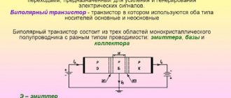
It is worth noting that bipolar transistors with an insulated gate must be checked according to the circuit described above for a field device. Keep in mind that drain and source are collector and emitter.
Expert opinion
Viktor Pavlovich Strebizh, lighting and electrical expert
Any questions ask me, I will help!
The device should show a slight voltage drop, or even a short circuit; some devices beep happily. If there is something you don’t understand, write to me!
Circuit for checking an n-channel field-effect transistor with a multimeter
Before checking the serviceability of the field-effect transistor, it is necessary to take into account that in modern MOSFET-type radio components there is an additional diode between the drain and the source. This element is usually present on the device diagram. Its polarity depends on the type of transistor.
The procedure for checking the serviceability of an n-channel transistor with a multimeter is as follows:
- Remove static electricity from the transistor.
- Set the multimeter to diode test mode.
- Connect the black lead of the multimeter to the minus of the measuring device, and the red lead to the plus.
- Connect the red wire to the source, and the black wire to the drain of the transistor. If the transistor is working properly, the multimeter will show a voltage at the junction of 0.5 - 0.7 V.
- Connect the red lead of the multimeter to the drain, and the black lead to the source of the transistor. If the device is working properly, the multimeter will show one, which means infinity.
- Connect the black wire to the source and the red wire to the gate. Thus, the transistor opens.
- The black wire is left at the source, and the red wire is connected to the drain. If the device is working properly, the multimeter will show a voltage from 0 to 800 mV.
- When changing the polarity of the multimeter probes, the readings should not change.
- Connect the red wire to the source and the black wire to the gate. The transistor will close.
- In this case, the transistor will return to the state corresponding to paragraphs 4 and 5.
Based on the measurements taken, we can conclude that if the field-effect transistor opens and closes using a constant voltage from a multimeter, then it is working.
This is used when checking a transistor, when it is first opened with the voltage of a multimeter (item 6), and then for some time, until the input capacitance is discharged, additional measurements are taken (items 7,8).
How to check kp303.
- Place the probes in their places. We advise you to carefully study the instructions for the multimeter so that you know which socket is intended for what. Typically, the hole marked “COM” is intended for the black probe, and “VΩmA” for the red one. If your multimeter has such sockets, connect it.
- Select the desired function: resistance test. In the second case, you can set the limit to 2 kOhm. The resistance test mode is essentially an ohmmeter. Therefore, if you are looking for how to test a transistor with an ohmmeter, but you do not have such a device separately, feel free to use a multimeter with this function.
How to check a transistor with a multimeter without desoldering
If you are thinking about how to test a transistor on a board with a multimeter, then remember that only bipolar elements can be determined in this way. But we advise you not to do this either, because in some cases the pn junction of the part is shunted with a low-resistance resistance. Because of this, the result is unlikely to be accurate. This means that desoldering is a necessity.
This is the minimum you needed to know about checking a transistor with a multimeter without desoldering.
We hope that our article was useful to you. Check out other materials on our blog. We have a lot of important information in store for you!