Triggers of various types are often included in various simple circuit designs that do not require the use of microcontrollers. They can save previously set values, change them, and record a logical zero or one. The D-trigger is one of the most common types of such devices. It allows you to delay signals, as well as store information for the required time.
What are the triggers?
The action of triggers is based on certain principles, depending on their type. These logic devices receive input signals that control them. The output information depends on the signal received at the input and on the one received at the previous stage. Consequently, the D-flip-flop reacts both to currently existing values and to previously received ones.
The graphical designation (UGO) of a D-flip-flop demonstrates that its input D is informational, and the second, designated by the letter C, is used to synchronize recording and allows you to save at the output the state that was at the input at the time it changed to 1 (which called "transparency" mode).
A trigger can be synchronous (clocked) or asynchronous (unclocked). In the first case, the device takes into account clock signals. In any computing system, all actions are performed in relation to signals of this type in order to ensure consistent operation.
The use of clock signals in synchronous flip-flops means that operation according to the underlying principle does not occur at any time, but only when a certain event is observed at the control input. For example, if a clock pulse transitions from the maximum value to zero or vice versa. Asynchronous devices do not have such a binding. In them, the transition from one mode to another is accomplished by a voltage drop.
Triggers are quite complex electronic circuits, but they provide a simple and understandable principle for converting input signals into output signals. D-flip-flops are also called “latches,” which clearly explains their operating principle.
What is D trigger
Triggers are devices that can maintain a certain output state for a long time. Typically, they control appropriate voltage levels. Changes occur with a certain combination of input signals.
The simplest devices in this category are created according to the RS scheme. They remember the state of the signal applied to one of the inputs. To eliminate the process of failures, which are caused by parasitic oscillations when the signal transitions from zero to one and back, synchronization is used. This additional signal sets the exact time (interval) for possible changes.
The designation D of the trigger indicates the main feature. The letter “D” (D in Latin) marks the input to which the information signal is supplied. The other (“C”) is used for recording synchronization. Lack of activity on it excludes a change in the basic state. This solution, unlike RS, allows you to change state using only one data source.
How does a D-trigger work?
The D-trigger inputs are divided into information (control) and auxiliary. The latter are designed to synchronize the operation of the device. The first set a certain combination of binary numbers at the input, which will be taken into account when generating the output signal. The clock signal controls the operating logic. It is he who determines the moment the trigger is triggered, and the state of the output signal depends on its characteristics.
A D flip-flop is also called a delay flip-flop because it is capable of delaying the input information signal by one clock cycle. The delay time is determined by the frequency of the synchronization pulses. If the information signal changes, the output will repeat its change, but only after the clock signal takes a value equal to one. As long as its value remains zero, the output signal will not change.
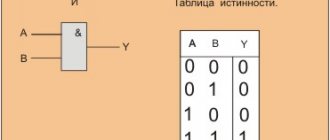
The operation of any D flip-flop is reflected in the truth table. As you can see, the truth table of a static D flip-flop is quite simple. It shows that a zero value of the control signal ensures that the previous value of the output signal is stored for any desired period of time. In practice, we are talking about the time when power is connected to the device.
The presented truth table provides information about the operation of a D-flip-flop at a value of C = 1. In practice, another option is used when operation occurs on the leading edge of the pulse. That is, the output value becomes equal to the input value at the moment when the value of the control pulse changes from zero to 1. A logic element that uses control by voltage level is called a static D-trigger, and by the edge - dynamic.
When edge control is used, triggering occurs when the control value changes. Two options can be used: leading edge or trailing edge. When using the first option, the value changes from 0 to 1, the second - from 1 to 0.
In addition to the table, timing diagrams are also used to describe the operation of logical elements.
A more complicated version of the trigger
Sometimes a more complicated version is used when another input is added. It is usually designated by the letter R. If a signal with a zero value is applied to it, it has no effect on the operation of the element. In the case when a signal with a single value is received at input R, Q is reset to 0. The same can be achieved on a classic D flip-flop if you use C = 0 and D = 0.
D-flip-flop implementation schemes
There are different options for constructing this logical element. Below is a diagram of a single-stage D flip-flop using NAND elements. Its inputs are direct static. The elements designated DD1.1 and DD1.2 are involved in the control circuit, and the rest are used as an asynchronous RS trigger.
The role of each element will be easier to understand by studying the principle of operation of the D-trigger. From the diagram it can be seen that if C = 0, then the logical AND operation will create a zero value regardless of the second input values on DD1.1 and DD1.2. The negation operation will produce a one at the output of both of these elements.
At the input of the third element there will be two values: one and the negation of Q. The AND operation at the output will form the negation of Q. The negation will lead to the fact that the output will have a Q value that coincides with the one that was here before.
The fourth element will receive one and Q. The result of applying AND will be Q. After applying negation, the output of this element will be the negation of Q. Therefore, in this case the value will not change.
Now we need to consider the situation when the control input has a single value. If D = 0, then after applying AND a zero will be obtained, and as a result of negation, the output value of DD.1 will become one, which will be transmitted to the input of DD1.2.
In DD1.2 there are two ones at the input, which means the AND operation will generate 1, and negation will give 0. Therefore, at DD1.4 the output will be one, which corresponds to a zero value of Q. The remaining options are calculated using the same principle.
The D-trigger circuit can be obtained from a synchronous RS-trigger by introducing an additional AND-NOT element, connecting both inverse inputs into one information input. This eliminates the state of uncertainty for S and R.
There are also combined D-triggers. They have inputs S and R, intended for asynchronous setting of logical 0 and 1. Using these inputs, the device can be given an initial specific state.
The diagram shows that a D-flip-flop is built from 6 AND-NOT elements; its operating principle is as follows: if there is a 1 at the input R and a zero at C, D, S, elements from the first to the fifth will remain closed. The sixth element will be open, that is, Q = 1, and /Q = 0. The first element will open if the zero signal is removed from the S input. The state of the remaining elements will not change.
When a single signal arrives at input C, the same signal will appear at all inputs of the third element, causing it to open. The sixth element will close and /Q = 1. Then single signals will also arrive at the inputs of the fifth element, and it will assume an open state, and Q = 0. As a result, after switching the trigger, a signal identical to the signal that was at the input will appear at the output Q D before switching, that is, Qn+1 = Dn = 0. If a single signal is removed from input C, the state of the trigger does not change.
The D-trigger circuit is quite simply implemented on CMOS chips. In such devices, the functions of logical elements AND are performed by ordinary transistor switches.
After a high-level clock signal arrives at input C, transistor No. 1 opens, providing a signal from D to Q. This activates the first inverter. In this situation, the second transistor remains closed. It turns off the inverter, built on transistors VT1 and VT3. This inverter turns on after a low potential arrives at input C.
D-flip-flops are included in many microcircuits. For example, the TM2 chip contains two such elements, TM5, TM7, TM8 - four, TM9 - six.
Trigger device
Pulse duty cycle
It is easiest to imagine functionality based on elementary logic elements. The second name for triggers in this category is “latch”, which clearly explains the basic principles of operation.
D trigger circuit
In addition to the main ones, the figure shows the entrances. Regardless of the synchronization signals, they are used to transfer the product to the zero or one state. This implements the priority principle, since activating S and R blocks the C input gates.
Application of D-flip-flops
The ability to store information allows the use of D-flip-flops to implement memory devices. These operating elements are capable of maintaining the desired output mode until a control signal is applied to change it. A trigger makes it possible to both enter binary information and store and read it.
Understanding what a D flip-flop is, it can be used to create a latch register. These devices are important in certain situations. Sometimes the signal lasts for a very short period of time and the microcircuit may not have time to react to it. In such cases, it is advantageous to use another chip, which will store the necessary values for a time sufficient to perform the necessary actions.
One of the main purposes of a D-flip-flop is to be used in counting mode. To make it work as a pulse counter, it is enough to apply a signal to input D from its own inverter output. In this mode, upon arrival of each pulse at input C, the trigger will change its state to the opposite, as shown in the timing diagram.
A frequency divider is a device that can change the frequency of the output signal relative to the input value. Using a cascade connection of several elements, it is possible to build frequency dividers with different division ratios. Two D flip-flops connected in series produce an output signal that is one-fourth the frequency of the input. Three elements connected in series will divide it by eight, and four elements will divide it by sixteen.
When creating digital circuits, the operation of which is synchronized by a single clock generator, it is often necessary to achieve synchronization of the operating circuit and the external input signal. That is, an asynchronous signal must be converted into a synchronous one for the entire system into which it enters. This problem can be solved by installing a D-trigger.
A trigger is capable of performing a logical function and at the same time maintaining feedback. That is why it is used to create many devices designed to remember, store, transmit and convert information. These elements can be found in a wide variety of devices, including digital microelectronics devices.
2.9.3. Trigger with counting input (t-flip-flop)
The main feature of the T-trigger is that when the next pulse arrives at its input, the trigger changes its state to the opposite. There are two structures of T-flip-flops: single-cycle and push-pull. Single-cycle circuits are currently practically not used due to their lack of reliability.
In Fig. Figure 2.36 shows a logical circuit of a T-flip-flop with a counting input, built on the “AND-OR-NOT” element base. As can be seen from the diagram, the outputs of the Q flip-flop are connected to the inputs by feedback.
Rice. 2.36. Logic circuit of a push-pull T flip-flop
A push-pull circuit is used to use feedback to create a mechanism for remembering the previous state of the trigger for the duration of the transition process when the first stage trigger is set to the opposite state.
The UGO of the T-trigger is shown in Fig. 2.36. As can be seen from the timing diagram (Fig. 2.37), when the next pulse arrives at the counting input of the trigger, its state changes to the opposite. In this case, between the moments of triggering of the triggers of the first and second stages there is a time delay equal to the duration of the synchronization pulse. The frequency of the pulses arriving at the trigger input is divided by two, i.e. the trigger itself fires 2 times less often.
Rice. 2.37. Timing diagram of T-trigger operation
In table Figure 2.16 shows the transition table of a flip-flop with a counting input. In it, the symbol “┐” denotes the inversion of the Q signal.
Fig.2.38. UGO T-trigger
Table 2.16
| Сt | Q1t+0.5 | Qt+1 |
| 0 | Q1t | Qt |
| 1 | ┐Qt | ┐Qt |
2.9.4. Universal d-trigger (trigger-delay)
Its peculiarity is that it has one information input (name D for Delay). The trigger remembers (delays) information that arrives through one information channel. A trigger is also called a universal trigger because all other types of triggers can be built on its basis. There are two D flip-flop structures: single-cycle and push-pull.
In Fig. Figure 2.39 shows the UGO of a single-cycle D-flip-flop.
Rice. 2.39. UGO single-ended D-flip-flop
Rice. 2.40. Single-ended D flip-flop logic circuit
In Fig. Figure 2.40 shows the logical circuit of a D-flip-flop, built on an LE of the “AND-NOT” type. The peculiarity of this circuit is that there is only one information input D.
In table Figure 2.17 shows the transition table of a single-ended D-flip-flop.
Table 2.17
| D | Ct | St | Rt | Qt+1 |
| 1 | 1 | 0 | 1 | 1 |
| 0 | 1 | 1 | 0 | 0 |
| 1 | 0 | 1 | 1 | Qt |
| 0 | 0 | 1 | 1 | Qt |
From this table it can be seen that when C = 1, the output of the trigger is set to a state equal to the value of input D.
Rice. 2.41. Logic circuit of a push-pull D flip-flop
In Fig. Figure 2.41 shows the logical diagram of a push-pull D flip-flop built on the “NAND” element base.
The UGO of a push-pull D-trigger is shown in Fig. 8.13. This circuit differs from a push-pull RS flip-flop in that it has only one information input D.
Rice. 2.42. UGO push-pull D-trigger
Rice. 2.43. T-flip-flop based on push-pull D-flip-flop
Based on a push-pull D-trigger, a T-trigger can be built, with input C playing the role of a counting input (Fig. 2.43).
studfiles.net