CONTENT
In cases where the purpose of testing is to select the best triode samples from a given batch, the testing process consists of measuring the reverse collector current (Fig. 1) and determining the gain β (Fig. 2). The current gain of a transistor connected according to a circuit with a common emitter is found using the formula
| Rice. 1. Connection diagram of a transistor with a power source and a milliammeter when measuring the reverse collector current | Rice. 2. Circuit for determining the current gain β |
β = (R/U)Ik ,
where R the resistance of the resistor, kOhm , U is the voltage of the power source (for example, a battery for a flashlight), V , I is the collector current, mA .
The values of and are usually chosen within the range R = 5-90 kOhm and U = 1.5-9 V.
To facilitate the calculation of the coefficient β , the resistance of the resistor and the voltage of the power source are selected such that their ratio is equal to an integer multiple of ten, for example, 10, 20, 30, etc.
When choosing the values of R , Rolim and and take into account the fact that the current
Ik = βpr U(B) / R (kOhm) ,
where β pr is the expected maximum value of β , should not exceed the maximum collector current permissible for this type of transistor, and the resistance of the resistor Rolim , which limits the current through the milliammeter in the case of connecting the collector to the emitter, should be approximately equal to U/7I0 , where U is the source voltage supply in volts, I0 is the current of the total deviation of the milliammeter in amperes.
In the absence of a milliammeter, you can measure the gain β of a low-power transistor using an ohmmeter. They do it like this.
Connect the conductors of the ohmmeter to each other and set the arrow of the device to the zero mark of the scale.
Then assemble the circuit shown in Fig. 3a, move the switch slider to position 3-1 and note the first ohmmeter reading Ω1 . After this, move the slider to position 3-2 and set the slider of resistor R2 to a position at which the ohmmeter reading increases by 1000 Ohms, that is, it becomes equal to Ω1 + 1000 .
Rice. 3. Connection diagram of devices when measuring current gain β using an ohmmeter
Having completed these measurements, turn off the ohmmeter, measure the resistance of resistor R2 and calculate the required value using the approximate formula:
β = 0.001 (R2 - R1)
In cases where a batch of transistors is being tested for amplification ability, it is desirable to simplify the measurement process. This can be achieved by introducing a second resistor R1 (Fig. 3.6).
In this case, the difference in resistance of sections 2-4 and 1-4 is equal to (R2 + R1) - R1 = R2 and the formula for calculating β takes the simple form:
β = 0.001 R2
From the last expression it is easy to see that the diagram in Fig. 3b allows you to determine the gain β by simply reading it from the scale of resistor R2 . To do this, you only need to calibrate the resistor in tens of kilo-ohms.
[/td]
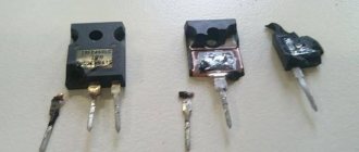
A simple and reliable way to test transistors, as well as a method for selecting the best samples from available batches of triodes, is to test a semiconductor triode in a mock-up of some generator. If, when the transistor is inserted into the circuit and the power source is turned on, the generator immediately starts working, then the transistor under test is considered to be in good working order. Its quality is judged by the reading of an alternating current voltmeter connected to the collector-emitter of the lower transistor through a capacitor with a capacity of 4700-6800 pF . The greater the angle of deflection of the instrument needle, the better the transistor being tested.
ABC of MOSFET Device
In general terms, a MOSFET allows a low gate voltage to control the current flowing through the source-drain channel. Thanks to this property, it is possible to significantly simplify the control circuit, as well as reduce the total power spent on control.
Today, two MOSFET production technologies are widely used: planar and Trench.
The first MOSFETs were created using planar technology. Transistors manufactured using this technology are shown in Fig. 1. Their structure consists of a metal and a semiconductor separated by a layer of silicon oxide SiO2.
Rice. 1. Planar technology - the first discrete MOSFETs
The Trench structure (Fig. 2) has a higher cell density, which is expressed in a lower Rds(on) value. In Trench MOSFET, a V-shaped groove is created on the surface of the substrate, onto which an oxide layer is deposited, and then metallization occurs.
Rice. 2. High-density Trench MOSFETs can be smaller than their planar counterparts but have comparable Rds(on) values.
The gate field in a Trench MOSFET affects a much larger area of the silicon. As a result, smaller physical dimensions are required to obtain the same Rds(on) than when manufacturing MOSFETs using planar technology.
Along with the obvious advantages, MOSFETs also have negative sides. Thus, an internal diode is formed between the n- drain and p+ source layers. The characteristics of this diode are given in the technical data for all MOSFETs. When using MOSFETs in switching circuits, the reverse recovery time of the internal diode must always be taken into account. Also, an internal NPN transistor is formed in the MOSFET, the collector of which is the n-drain layer, the base is the p-layer, and the emitter is the n-source layer.
It must be taken into account that the metallization of the source (Fig. 3) in some places has a very low resistance between the base-emitter junction; this point complicates the switching on of the transistor.
Rice. 3. Internal diode and bipolar transistor in MOSFET structure
Types, classification of transistors
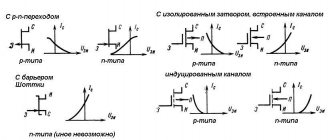
We avoid exploring the wilds. Know a simple rule: in bipolar transistors, carriers of both signs participate in creating the output current, in field-effect transistors - one. Definition of smart guys. Now we work with our fingers:
- Field-effect transistors are the beginning. When the Beatles took the stage, semiconductors began to replace vacuum triodes. In short, a pnp transistor is two crystal layers rich in positive carriers (silicon, germanium, impurity conductivity). While teaching physics lessons, the teacher often talked about how V-valent arsenic doped the silicon lattice, forming a new material. Let us add that the positive p-regions are fenced off by a narrow negative one (n-negative). Like a lump in my throat. A narrow isthmus, called the base, refuses to allow electrons (in our case, more like holes) to flow in the desired direction. A small negative charge appears on the control electrode, the collector holes (the upper p-region on traditional electrical circuits) can no longer be contained, literally tearing towards the applied voltage. Since the base is thin, using the accumulated speed, the carriers fly over the isthmus and are carried further - reaching the emitter (lower p-region), here they are carried away by the potential difference created by the supply voltage. Typical school explanation. The relatively small voltage of the control electrode is able to regulate the speed of a strong flow of holes (positive carriers) entrained by the supply voltage field. This is what the technology is built on. Electrons move towards the holes; transistors are called bipolar.
- Field-effect transistors are equipped with a channel of any type of conductivity that separates the source and drain regions (see figure above). The control electrode is called a gate. Moreover, the main material of the substrate, the gate, is opposite to the channel, source and drain. Therefore, positive voltage (see figure) prohibits the flow of charges through the transistor. The plus will pull (to the p-region) available electrons. Field-effect transistors are used much more often in electronics. In the figure, the gate is electrically connected to the crystal, the structure is called a control pn junction. It happens that the region is isolated from the crystal by a dielectric, which is often an oxide. Pure MOSFET transistor, in Russian - MOS.
Transistor test circuit
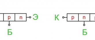
Using a multimeter, bipolar transistors are checked in normal mode. If the tester supports such an option, often called hFE, a round connector is mounted on the front panel, divided by a vertical line into two parts, where 4 sockets are labeled as follows:
- B – base.
- C – collector.
- E – emitter.
There are two emitter sockets to take into account the layout of the housing pins. The base can be on the edge or in the middle. Made for convenience. It makes no difference which socket the emitter leg of the bipolar transistor is inserted into. A few words on how to use it.
Checking the transistor with an ohmmeter
Since the transistor contains two pn junctions, their serviceability can be checked using the method used for testing semiconductor diodes. To do this, it can be thought of as the equivalent of a back-to-back connection of two semiconductor diodes.
The serviceability criteria for them are:
- Low (hundreds of Ohms) resistance when connecting a DC source in the forward direction;
- Infinitely high resistance when connecting a DC source in the reverse direction.
A multimeter or tester measures resistance using its own auxiliary power source - a battery. Its voltage is small, but it is enough to open the pn junction. By changing the polarity of connecting the probes from the multimeter to a working semiconductor diode, in one position we get a resistance of a hundred Ohms, and in the other - infinitely large.
A semiconductor diode is rejected if
- in both directions the device will show a break or zero;
- in the opposite direction, the device will show any significant resistance value, but not infinity;
- The device readings will be unstable.
When checking a transistor, six resistance measurements with a multimeter will be required:
- base-emitter direct;
- base-collector direct;
- base-emitter reverse;
- base-collector reverse;
- emitter-collector direct;
- emitter-collector reverse.
The criterion for serviceability when measuring the resistance of the collector-emitter section is an open circuit (infinity) in both directions.
Linear operating mode
Let's consider the operation of MOSFET in linear mode.
In Fig. 11, on a logarithmic scale, the values of the drain-source voltage VDS are plotted on the horizontal axis, and the drain current values ID are plotted on the vertical axis. The safe operating region curve describes the forward-biased characteristic of a MOSFET transistor.
Rice. 11. MOSFET safe mode area
A positive slope in the first decade of ID/VDS reflects constant resistance RDS(ON), negative - constant power. At low voltage, the MOSFET cannot conduct rated current due to the RDS(ON) channel resistance and low VDS value. The constant resistance RDS(ON) is shown linearly in the first part of the curves (green line) of the safe operation region.
The second part of the curve (gray line) reflects the maximum current through the transistor. The third part (blue line) is the constant power of the MOSFET.
The fourth part (the lines of pink and purple colors) has never been described, with the exception of the most recent technical descriptions from the IR company. This segment has a negative slope above constant power. In essence, this looks like a secondary breakdown in a bipolar transistor, but it is not. This shows the region of stable operation of the transistor in a stable state - the voltage VDS is higher, and the current ID is lower than the maximum permissible. Most pulse devices do not operate in this state. In a switching power supply, the transistor is either on, with low VDS and high current (top left line of the safe operating region), or off.
The second break point on the safe operating area curve shows the Spirito limit. This inflection point occurs due to the microscopic features of the transistor. A MOSFET consists of many thousands of parallel cells, each cell having approximately the same VDS and VGS values. The only parameter that distinguishes a cell from a cell is the gain. When the MOSFET is in saturation mode, the difference in gain is not significant. But this is noticeable in linear mode. A cell with higher gain passes more current, causing local overheating. The solution is to put the transistor into saturation, then the cells optimally distribute the current without causing overheating. Early planar MOSFETs operate most optimally in linear mode. With low cell density and low gain, they better distribute heat flow over a large area, which has less impact on MOSFET performance in linear mode. Early planar transistors (Fig. 12) are better suited for linear operating modes than Trench devices.
Rice. 12. Comparison of technologies when operating in linear mode
This is best illustrated by comparing three different process technologies - early planar technology, updated planar technology, and Trench technology.
For MOSFETs operating in linear mode with a constant gate-to-source voltage VGS, drain current ID and temperature, increasing the temperature (keeping VGS constant) and increasing the current leads to thermal runaway and instability. Conversely, a decrease in current with increasing temperature leads to an increase in the stability of transistors in linear mode.
The graph of early planar MOSFETs clearly shows the crossover point after which heating causes the same or less current for a given value of VGS. This effect is not observed with MOSFETs with updated planar technology and with Trench.
Updated planar and Trench-MOSFETs are not suitable for hot-swap and linear regulation technologies, as they will immediately leave linear mode. These applications require early planar MOSFET technology.
COMPEL application engineers can give you an answer about the production technology of a particular MOSFET and the possibility of its use in a particular circuit.
This review should help solve many problems when creating device prototypes. And although a large number of parameters and main directions were not touched upon, an attempt was made to explain the basic mechanisms, interactions, and possible ways to solve emerging problems. Whether designing a DC/DC converter or a hot-swap circuit, this material will be useful at all levels, from miniature to multi-watt devices.
International Rectifier engineers have developed a convenient online tool (located on the website https://www.irf.com/: Design Support ® SyncBuck MOSFET Tool) for selecting the optimal MOSFET pair for step-down synchronous converters. By entering all the data necessary for the calculation, you will receive a list of recommended transistors with a short list of their parameters, case type and estimated cost.
Obtaining technical information, ordering samples, delivery – e-mail
•••