Transistors: circuit, principle of operation, how bipolar and field-effect differ
The transistor is a ubiquitous and important component in modern microelectronics.
Its purpose is simple: it allows you to control a much stronger one using a weak signal. In particular, it can be used as a controlled “damper”: by the absence of a signal at the “gate”, block the flow of current, and by supplying it, allow it. In other words: this is a button that is pressed not by a finger, but by applying voltage. This is the most common application in digital electronics.
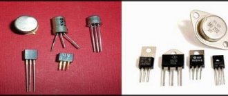
Transistors are available in different packages: the same transistor can look completely different in appearance. In prototyping, the most common cases are:
The designation on the diagrams also varies depending on the type of transistor and the designation standard used in the compilation. But regardless of the variation, its symbol remains recognizable.
Application of transistors in life
Transistors are used in many technical devices. The most striking examples:
- Amplifier circuits.
- Signal generators.
- Electronic keys.
It will be interesting➡ What is an LED
In all communication devices, signal amplification is necessary. First, electrical signals naturally attenuate. Secondly, it often happens that the amplitude of one of the signal parameters is not enough for the device to operate correctly.
Information is transmitted using electrical signals. In order for delivery to be guaranteed and the quality of information to be high, we need to strengthen the signals. Transistors can influence not only the amplitude, but also the shape of an electrical signal. Depending on the required shape of the generated signal, the appropriate type of semiconductor device will be installed in the generator. Electronic keys are needed to control the current strength in the circuit. These switches contain many transistors. Electronic keys are one of the most important elements of circuits.
They are the basis for computers, televisions and other electrical appliances, which are indispensable in modern life.
Evolution of the transistor
Bipolar transistors
Bipolar junction transistors (BJT, Bipolar Junction Transistors) have three contacts:
The main characteristic of a bipolar transistor is the hfe indicator, also known as gain. It reflects how many times more current in the collector-emitter section the transistor can pass in relation to the base-emitter current.
For example, if hfe = 100, and 0.1 mA passes through the base, then the transistor will pass a maximum of 10 mA through itself. If in this case there is a component in the high current section that consumes, for example, 8 mA, it will be provided with 8 mA, and the transistor will have a “reserve”. If there is a component that draws 20 mA, it will only be provided with the maximum 10 mA.
Also, the documentation for each transistor indicates the maximum permissible voltages and currents at the contacts. Exceeding these values leads to excessive heating and reduced service life, and a strong excess can lead to destruction.
NPN and PNP
The transistor described above is a so-called NPN transistor. It is called that because it consists of three layers of silicon connected in the order: Negative-Positive-Negative. Where negative is a silicon alloy with an excess of negative charge carriers (n-doped), and positive is an alloy with an excess of positive charge carriers (p-doped).
NPNs are more effective and common in industry.
When designating PNP transistors, they differ in the direction of the arrow. The arrow always points from P to N. PNP transistors have an “inverted” behavior: current is not blocked when the base is grounded and blocked when current flows through it.
Checking bipolar types
Below is a diagram for checking npn, pnp transistors with a tester, after which we will describe the procedure point by point.
The bipolar transistor is equipped with pn lines - conventionally, these are diodes, or rather, 2 of them located oppositely, the point of their intersection is the “base”.
One conditional diode is designed with base/collector contacts, the other with base/emitter contacts. For analysis, just look at the contrast. (directly and back) of the indicated areas: if there are no problems there, then the part is without flaws.
Do-it-yourself testing without soldering a bipolar pnp, npn transistor involves testing 3 combinations of legs:
pnp option
Structures (types) are shown by the arrow emitting. section: pnp/npn (to/from the base). Let's start by checking the first option. We open the PNP part by applying negative voltage to the base. On the multimeter, we set the selector to measure Ohms to o; it is also possible to set it to “continuity”.
The vein “−” (black) is on the base leg. Plus (red) - alternately to collect., emitter. If the areas are not damaged, they will display about 500–1200 Ohms.
Next we will describe how to ring the reverse resistance: “+” - to the base, “−” - to the call. and emits. High resistance should be displayed. on both pn sites. We now have “1”, that is, for the frame set to “2000” the value exceeds 2000. This means that there are 2 transitions without breaks, the product is in good working order.
It will be interesting➡ ShVVP wire and cable. Design features and application of the ShVVP cable
Similarly, as described, you can test the transistor for serviceability without removing it from the circuit. Less commonly, there are assemblies where substantial shunting is applied to the transitions, for example, with resistors. Then, if too low resistance is displayed, the part will need to be desoldered.
npn structure
Npn elements are checked in the same way, only the “+” probe goes to the base from the tester.
Symptoms of a problem
If the resistance (direct and reverse) of one of the sections (pn) tends to infinity, that is, at o and above on the display “1”, which means that this section has a break, the transistor is unusable. If “0” means the product is also flawed, the area is broken. Direct cont. there should be 500–1200 ohms.
Field effect transistors
Field effect transistors (FET, Field Effect Transistor) have the same purpose, but differ in internal structure. A particular type of these components are MOSFET (Metal-Oxide-Semiconductor Field Effect Transistor) transistors. They allow you to operate with much greater power with the same dimensions. And the control of the “damper” itself is carried out exclusively using voltage: no current flows through the gate, unlike bipolar transistors.
Field effect transistors have three contacts:
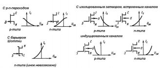
N-Channel and P-Channel
By analogy with bipolar transistors, field transistors differ in polarity. The N-Channel transistor was described above. They are the most common.
P-Channel when designated differs in the direction of the arrow and, again, has an “inverted” behavior.
Connecting transistors to drive high-power components
A typical task of a microcontroller is to turn a specific circuit component on and off. The microcontroller itself usually has modest power handling characteristics. So Arduino, with 5 V output per pin, can withstand a current of 40 mA. Powerful motors or ultra-bright LEDs can draw hundreds of milliamps. When connecting such loads directly, the chip can quickly fail. In addition, for the operation of some components, a voltage greater than 5 V is required, and Arduino cannot produce more than 5 V from the digital output pin.
But it is easily enough to control a transistor, which in turn will control a large current. Let's say we need to connect a long LED strip that requires 12 V and consumes 100 mA:
Now, when the output is set to logical one (high), the 5 V entering the base will open the transistor and current will flow through the tape - it will glow. When the output is set to logic zero (low), the base will be grounded through the microcontroller and current flow will be blocked.
Pay attention to the current-limiting resistor R. It is necessary so that when the control voltage is applied, a short circuit does not form along the microcontroller-transistor-ground route. The main thing is not to exceed the permissible current through the Arduino contact of 40 mA, so you need to use a resistor with a value of at least:
here Ud is the voltage drop across the transistor itself. It depends on the material from which it is made and is usually 0.3 – 0.6 V.
But it is absolutely not necessary to keep the current at the permissible limit. It is only necessary that the gain of the transistor allows you to control the required current. In our case, this is 100 mA. Let's say for the transistor used hfe = 100, then a control current of 1 mA will be enough for us
A resistor with a value from 118 Ohm to 4.7 kOhm is suitable for us. For stable operation on one side and light load on the chip on the other, 2.2 kOhm is a good choice.
If you use a field-effect transistor instead of a bipolar transistor, you can do without a resistor:
This is due to the fact that the gate in such transistors is controlled solely by voltage: there is no current in the microcontroller - gate - source section. And due to its high characteristics, a circuit using MOSFETs allows you to drive very powerful components.
Transistor functions
Transistors perform the following functions:
- Allows you to amplify electrical signals. Transistors amplify any electrical signals, both high and low frequencies.
- They can work like a key, turning on and off the flow of electric current. This simple on/off switch makes all modern processors work. Transistors are the basis of all modern digital technology.
- Generate electrical signals due to positive feedback. Based on them, you can make sound and signal generators.
- They can match the resistance of electrical circuits due to various switching schemes and work as current limiters. In power supplies, transistors can limit short-circuit current and also act as a fuse.
How are transistors inferior to lamps?
Despite the undeniable advantages of transistors over tubes, tube triodes still have a number of advantages, including:
- Resistance to high electromagnetic interference and interference. This does not mean that semiconductor technology can fail from any interference. But if a strong magnetic storm from the Sun occurs (or a powerful EMP strike from nuclear bombs), then all pn junctions in semiconductor technology may fail due to high pickup currents. Vacuum technology is much more resistant to such interference.
- Tube technology works much better and more stable at high frequencies. And these are already design features. Since transistors have pn junctions, they also have their own capacitance. And parasitic capacitance at high frequencies negatively affects signal amplification. Nonlinear distortions appear. And in vacuum technology there are lamps that have several shielding meshes, which reduce the effect of parasitic capacitances. An example of a radio tube is a klystron.
It cannot be said outright that transistors have completely eradicated tubes. Each part has its own advantages and disadvantages in different areas. Of course, in digital technology, transistors have no equal among tubes. However, at ultra-high frequencies, transistors are still inferior to tubes.
Post Views: 480
What is the difference between a field-effect transistor and a bipolar one?
What parameters determine the properties of a transistor in its performance?
The transistors operate between the active mode and the cutoff mode, as a result of which the circuit does not enter saturation mode, which increases its performance.
The performance of the transistor depends only on the rate of recharging of the barrier capacitance. The reason for the inertia of a bipolar transistor is the finite time of charge transfer from the emitter junction to the collector and the parasitic capacitances of these junctions. And the performance, in turn, depends on how strong the inertial properties are.
The speed of the transistor is determined by the switching time of the transistor switches, and the specific conductivity (and speed) depends on the concentration of charge carriers and their mobility.
The speed of the transistor is determined by the switching time of the transistor switches, or valves, which is inversely proportional to the power consumption P: = A/P. Here A is the key operation for one switching. Increasing power in order to speed up switching, as a rule, requires increasing the distance between individual circuit elements to maintain the required thermal conditions, which leads to a decrease in the density of the elements and an increase in the delay in signal propagation along the lines.
The power dissipated in the crystal as heat must be less than the thermal power that can be removed.
A field-effect transistor differs from a bipolar transistor, firstly, in its operating principle: in a bipolar transistor, the output signal is controlled by the input current, and in a field-effect transistor, by the input voltage or electric field. Secondly, field-effect transistors have significantly higher input resistances, which is associated with the reverse bias of the gate pn junction in the type of field-effect transistors under consideration. Thirdly, field-effect transistors can have a low noise level (especially at low frequencies), since field-effect transistors do not use the phenomenon of injection of minority charge carriers and the field-effect transistor channel can be separated from the surface of the semiconductor crystal. The processes of carrier recombination in the pn junction and in the base of the bipolar transistor, as well as generation-recombination processes on the surface of the semiconductor crystal, are accompanied by the appearance of low-frequency noise.
Advantages and disadvantages of composite transistors
The power and complexity of a Darlington transistor can be adjusted by increasing the number of bipolar transistors included in it. There is also an IGBT transistor, which includes a bipolar transistor and a field effect transistor, used in the field of high voltage electronics.
The main advantage of composite transistors is their ability to provide high current gain. The fact is that if the gain of each of the two transistors is 60, then when they work together in a composite transistor, the total gain will be equal to the product of the coefficients of the transistors included in its composition (in this case, 3600). As a result, a fairly small base current is required to open the Darlington transistor.
The disadvantage of composite transistors is their low operating speed, which makes them suitable for use only in circuits operating at low frequencies. Often, composite transistors appear as a component of the output stages of powerful low-frequency amplifiers.
Next
MiscellaneousLine voltage
Operating principle
Semiconductors occupy an intermediate state between conductors and dielectrics. In their normal state they do not conduct electricity, but their resistance decreases with increasing temperature. The higher it is, the more energy the substance receives.
In semiconductor atoms, electrons break away from the “parent” atom and fly away to another to fill the “hole” left by the same electron. It turns out that two processes occur simultaneously inside such a material: the flight of electrons (n-conductivity, from the word negative), and the formation of “holes” (p-conductivity from the word positive). In an ordinary piece of silicon, these processes are balanced: the number of holes is equal to the number of free electrons.
However, with the help of special substances, this balance can be disrupted by adding “extra” electrons (donor substances) or “extra” “holes” (acceptor substances). In this way, it is possible to obtain a semiconductor crystal with predominant n-conductivity or p-conductivity.
If two such materials are applied to each other, then a so-called pn junction is formed at the point of their contact. Holes and electrons pass through it, saturating its neighbor. That is, where there was an excess of holes, they are filled with electrons and vice versa.
At some point, there will be no free charge carriers left at the point of contact and equilibrium will occur. This is a kind of barrier that cannot be overcome, a kind of desert. This layer is usually called the depletion layer.
Now, if you apply voltage to such a material, it will behave in an interesting way: if it is directed directly, the depleted layer will become thinner and an electric current will flow through it, and if it is directed in the opposite direction, it will expand.
As they say, for dummies, a pn junction has the ability to pass current in only one direction. This is a kind of “check valve” for the electrical network. The operation of all semiconductor devices is based on this property.
There are two main types of transistors: field-effect transistors (sometimes called unipolar) and bipolar. They differ in structure and principle of operation.
Bipolar transistor
A bipolar transistor has two junctions: pnp or npn. The fundamental difference between them is the direction of current flow.
The collector and emitter, which have the same conductivity (in an npn transistor, n-conductivity), are separated by a base, which has p-conductivity. Even if the emitter is connected to a power source, it cannot penetrate directly into the collector. To do this, you need to apply current to the base.
In this case, electrons from the emitter fill the “holes” of the latter. But since the base is lightly doped, there are few holes in it. Therefore, most of the electrons go to the collector and they begin their movement along the circuit. The collector current is almost equal to the emitter current, because the base accounts for a very small value.
To visualize this more clearly, you can use the analogy of a water pipe. To control the amount of water you need a valve (transistor). If you apply a little force to it, it will increase its flow area of the pipe and more water will begin to flow through it.
What is an NPN transistor?
Transistors replaced electric lamps and made it possible to reduce the number of relays and switches in devices. These are semiconductor triodes - radio-electronic components made from semiconductors; they have 3 terminals as standard.
Transistors are designed to control current, that is, the main power factor of electrical circuits; it is its shock (not voltage) that poses a danger to humans.
The element is capable of controlling extremely high values in output circuits when applying a weak input signal. Transistors boost, generate, switch, and convert electrical signals; they are the basis of microelectronics and electrical devices.
Varieties based on operating principle:
- bipolar transistor made of 2 types of conductors, the basis of its operation is the interaction of adjacent pn sections on the crystal. They consist of an emitter/collector/base (hereinafter, we will abbreviate these terms): the latter receives a weak current, causing a modification of the resistance (hereinafter referred to as “resistance”) in the line consisting of the first 2 elements. Thus, the flowing quantity changes, the side of its unidirectionality (npn or pnp) is determined by the characteristics of the transitions (sections) in accordance with the polarity of the connection (reverse, forward). Control is carried out by modulating the current on the base/emitter segment, the output of the latter is always common for control and output signals;
- field. There is only one type of conductor - a narrow channel subject to the electric field of a separate gate passage. Control is based on modulating the number of volts between it and the source. And between the latter and the drain an electric current flows (2 working contacts). The value has a strength depending on the signals generated between the gate (control contact) and one of the specified parts. There are products with a pn control section (working contacts are connected to a p- or n-semiconductor) or with separate gates.
Field workers have polarity options; low voltage is required for control; due to their efficiency, they are installed in radio circuits with low-power power supplies. Bipolar variants are activated by currents. In analog assemblies, the latter (BT, BJT) prevail, in digital (processors, computers) - the former. There are also hybrids - IGBTs, used in power circuits.
Field-effect transistor
If in a bipolar transistor the control was carried out using current, then in a field-effect transistor it was controlled using voltage. It consists of a semiconductor plate, which is called a channel. On one side, a source is connected to it - through it, electric current carriers enter the channel, and on the other, a drain - through it they leave the channel.
The channel itself is, as it were, “sandwiched” between a gate, which has reverse conductivity, that is, if the channel has n-conductivity, then the gate has p-conductivity. The gate is electrically separated from the channel. By changing the gate voltage, you can adjust the pn junction area. The larger it is, the less electrical energy passes through the channel. There is a voltage value at which the gate will completely block the channel and the current between the source and drain will stop.
The most obvious illustration in this case is a garden hose that passes through the chamber of a small wheel. In this case, even when a small air pressure is supplied to it (gate-source voltage), it increases significantly in size and begins to pinch the hose, the lumen of the hose is blocked and the water supply stops (the pn junction area increases and electric current stops flowing through the channel).
The type of semiconductor device described above is classic and is called a transistor with a control pn junction. You can often find the abbreviation JFET - Junction FET, which is simply a translation of the Russian name into English.
Another type of field effect triode has a slight difference in gate design. On the silicon layer, a layer of dielectric silicon oxide is formed by oxidation. A shutter is already applied to it by metal spraying. The result is alternating layers of Metal - Dielectric - Semiconductor or MIS gate.
Such an insulated gate field effect transistor is designated by the Latin letters MOSFET.
There are two types of MIS shutter:
- An MIS gate with an induced (or inverse) channel is normally closed, that is, in the absence of voltage on the gate, no electric current passes through the channel. In order to open it, voltage must be applied to the gate.
- An MIS gate with a built-in (or its own) channel is normally open, that is, in the absence of voltage on the gate, electric current passes through the channel. In order to close it, voltage must be applied to the gate.
Main characteristics
The main feature of all types of transistors is the ability to control a powerful current using a small current. Their ratio shows how efficient the semiconductor device is.
In bipolar transistors, this indicator is called the static base current transfer coefficient. It characterizes how many times the main collector current is greater than the base current that caused it. This parameter has a very wide value and can reach 800.
Although at first glance it seems that the principle “the more the merrier” is important here, in reality this is not the case. Rather, the saying “less is more” applies here. On average, bipolar transistors have a base current transfer coefficient ranging from 10 to 50.
For field-effect transistors, a parameter of a similar type is called the slope of the input characteristic or the conductivity of direct current transmission. In short, it shows how much the voltage passing through a channel will change if the gate voltage is changed by 1 V.
If a signal with a certain frequency is applied to a transistor, it will amplify it many times over. This property of semiconductor devices is used in radio electronics. However, there is a frequency amplification limit beyond which the triode is no longer able to amplify the signal.
Therefore, the maximum operating frequency of the signal is considered optimal, 10-20 times lower than the maximum frequency gain of the transistor.
Another significant characteristic of a transistor is the maximum permissible power dissipation. The fact is that when any electrical device operates, heat is generated. The higher the current and voltage in the circuit, the greater it is.
It is removed in several ways: using special radiators, forced air flow, and others. Thus, there is a certain limit on the amount of heat for any triode (it is different for each) that it can dissipate into space. Therefore, when choosing a device, they proceed from the characteristics of the electrical circuit on which the transistor is to be installed.
Transistor connection circuits
Typically, a bipolar transistor is always used in direct connection - reverse polarity on a FE junction does not give anything interesting. For a direct connection scheme, there are three connection schemes: common emitter (CE), common collector (CC), and common base (CB). All three inclusions are shown below.
They explain only the operating principle itself - assuming that the operating point is somehow established, using an additional power source or auxiliary circuit. To open a silicon transistor (Si), it is necessary to have a potential of ~0.6 V between the emitter and the base, and for a germanium transistor ~0.3 V is enough.
Common emitter
Voltage U1 causes a current Ib, the collector current Ik is equal to the base current multiplied by β. In this case, the +E voltage should be quite large: 5 V-15 V. This circuit amplifies current and voltage well, and therefore power. The output signal is opposite in phase to the input signal (inverted). This is used in digital technology as the NOT function.
If the transistor does not operate in switching mode, but as an amplifier of small signals (active or linear mode), then by selecting the base current, set the voltage U2 equal to E/2 so that the output signal is not distorted. This application is used, for example, when amplifying audio signals in high-class amplifiers with low distortion and, as a result, low efficiency.
Common collector
In terms of voltage, the OK circuit does not amplify; here the gain is α ~ 1. Therefore, this circuit is called an emitter follower. The current in the emitter circuit is β+1 times greater than in the base circuit. This circuit amplifies current well and has low output impedance and very high input impedance.
Now is the time to remember that a transistor is called a resistance transformer. The emitter follower has properties and operating parameters that are very suitable for oscilloscope probes. It uses its huge input impedance and low output impedance, which is good for matching with a low-impedance cable.
Useful material: what is a semiconductor diode.
General base
This circuit has the lowest input resistance, but its current gain is equal to α. A circuit with a common base amplifies well in voltage, but not in power. Its feature is the elimination of the influence of capacitance feedback (Miller effect). Cascades with OB are ideally suited as input stages of amplifiers in radio frequency paths, matched at low resistances of 50 and 75 Ohms. Common base cascades are very widely used in microwave technology and their use in radio electronics with an emitter follower cascade is very common.
Types of transistors
The first transistors used germanium, which did not work very stably. Over time, it was abandoned in favor of other materials: silicon (the most common) and gallium arsenide. But these are all traditional semiconductors.
Currently, triodes based on organic materials and even substances of biological origin are beginning to gain popularity: proteins, peptides, chlorophyll molecules and entire viruses. Biotransistors are used in medicine and biotechnology.
Other classifications of transistors:
- Based on power, they are divided into low-power (up to 0.1 W), medium power (from 0.1 to 1 W) and simply powerful (over 1 W).
- They are also divided by housing material (metal or plastic), type of execution (in a housing, unpackaged, as part of integrated circuits).
- They are often combined with each other to improve performance. Such transistors are called composite or combined and can consist of two or more semiconductor devices. Their structure is simple: the emitter of the first is the base for the second and so on until the required number of triodes. There are several types: Darling (all components with the same type of conductivity), Sziklai (different type of conductivity), cascode amplifier (two devices working as one with a connection according to a circuit with a common emitter).
- The compound also includes an IGBT transistor, which is a bipolar one, which is controlled using a polar triode with an insulated gate. This type of semiconductor devices is used mainly where it is necessary to control high current (welding machines, city power grids) or electromechanical drives (electric vehicles).
- As control, not current, but another electromagnetic effect can be used. For example, phototransistors use a sensitive photocell as a base, and magnetotransistors use a material that induces a current when exposed to a magnetic field.
The technological limit for transistors has not yet been reached. Their size decreases with each goal, and various research institutes are searching for new materials for use as semiconductors. We can say that these semiconductor devices have not yet told the world their last word.
Bipolar transistor
Author: Vladimir Vasiliev · Published September 9, 2015 · Updated August 29, 2018
Greetings, dear friends! Today we will talk about bipolar transistors and the information will be useful primarily to beginners. So, if you are interested in what a transistor is, its operating principle and in general what it is used for, then take a more comfortable chair and come closer.
Let's continue, and we have content here, it will be more convenient to navigate the article
Bipolar transistor
The bipolar transistor is a descendant of tube triodes, those that were in televisions of the 20th century. Triodes went into oblivion and gave way to more functional brothers - transistors, or rather bipolar transistors.
With rare exceptions, triodes are used in equipment for music lovers.
Bipolar transistors may look like this.
As you can see, bipolar transistors have three terminals and structurally they can look completely different. But on electrical diagrams they look simple and always the same. And all this graphic splendor looks something like this.
This image of transistors is also called UGO (Conventional graphic symbol).
Moreover, bipolar transistors can have different types of conductivity. There are NPN type and PNP type transistors.
The difference between an NPN transistor and a PNP transistor is only that it is a “carrier” of electrical charge (electrons or “holes”). Those. For a pnp transistor, electrons move from the emitter to the collector and are driven by the base. For an NPN transistor, electrons go from the collector to the emitter and are controlled by the base. As a result, we come to the conclusion that in order to replace a transistor of one conductivity type with another in a circuit, it is enough to change the polarity of the applied voltage. Or stupidly change the polarity of the power source.
Bipolar transistors have three terminals: collector, emitter and base. I think that it will be difficult to get confused with the UGO, but in a real transistor it’s easier than ever to get confused.
Usually, where which pin is located is determined from a reference book, but you can simply ring the transistor with a multimeter. The terminals of the transistor sound like two diodes connected at a common point (in the area of the base of the transistor).
On the left is a picture for a pnp type transistor; when dialing, you get the feeling (through multimeter readings) that in front of you are two diodes that are connected at one point by their cathodes. For an NPN type transistor, the diodes at the base point are connected by their anodes. I think after experimenting with a multimeter it will be more clear.
NPN transistor circuit
When an NPN transistor is connected to voltage resources, base current will flow through the transistor. Even a small amount of base controls the circulation of a large amount of current through the emitter to the collector. The base voltage is higher than the emitter voltage.
It will be interesting➡ Capacitor charge
When VB base voltage is not -ve compared to VE emitter voltage, current cannot flow in the circuit. Therefore, it is necessary to provide a reverse bias voltage of >0.72 Volts.
Resistors RL and RB are included in the circuit. This limits the current passing through the maximum possible height of the transistor.
Emitter voltage VEB as input side. Here, the emitter current (IE) flows from the input side and flows in two directions; one is IB and the other is IC.
IE= YaB+ YaC
The principle of operation of a bipolar transistor
Now we will try to figure out how a transistor works. I will not go into details of the internal structure of transistors as this information will only confuse. Better take a look at this drawing.
This image best explains the working principle of a transistor. In this image, a person controls the collector current using a rheostat. He looks at the base current; if the base current increases, then the person also increases the collector current, taking into account the gain of the transistor h21E. If the base current drops, then the collector current will also decrease - the person will correct it using a rheostat.
This analogy has nothing to do with the actual operation of a transistor, but it makes it easier to understand the principles of its operation.
For transistors, rules can be noted to help make things easier to understand. (These rules are taken from the book “The Art of Circuit Design” by P. Horowitz W. Hill).
- The collector has a more positive potential than the emitter
- As I already said, the base-collector and base-emitter circuits work like diodes
- Each transistor is characterized by limiting values such as collector current, base current and collector-emitter voltage.
- If rules 1-3 are followed, then the collector current Ik is directly proportional to the base current Ib. This relationship can be written as a formula.
From this formula we can express the main property of a transistor - a small base current controls a large collector current.
- current gain.
It is also denoted as
Based on the above, the transistor can operate in four modes:
- Transistor cutoff mode - in this mode, the base-emitter junction is closed, this can happen when the base-emitter voltage is insufficient. As a result, there is no base current and therefore there will be no collector current either.
- The active mode of the transistor is the normal mode of operation of the transistor. In this mode, the base-emitter voltage is sufficient to cause the base-emitter junction to open. The base current is sufficient and the collector current is also available. The collector current is equal to the base current multiplied by the gain.
- Transistor saturation mode - the transistor enters this mode when the base current becomes so large that the power of the power source is simply not enough to further increase the collector current. In this mode, the collector current cannot increase following an increase in the base current.
- Inverse transistor mode - this mode is used extremely rarely. In this mode, the collector and emitter of the transistor are swapped. As a result of such manipulations, the gain of the transistor suffers greatly. The transistor was not originally designed to operate in such a special mode.
How does a transistor switch work?
In this article we will look at how a transistor switch on a bipolar transistor works. Such semiconductor elements are produced in two types - npn and pnp structures, which differ in the type of semiconductor used (in a p-semiconductor, positive charges - “holes" - predominate; in an n-semiconductor, negative charges - electrons).
The BT terminals are called base, collector and emitter, which have a graphical designation on electrical circuit drawings, as shown in the figure.
In order to understand the operating principle and individual processes occurring in bipolar transistors, they are depicted as two diodes connected in series and back-to-back.
The most common diagram of a BT operating in key mode is shown below.
To open a transistor switch, you need to apply potentials of a certain sign to both pn junctions. The collector-base junction must be reverse biased, and the base-emitter junction must be forward biased. To do this, the electrodes of the power supply UKE are connected to the terminals of the base and collector through a load resistor RK. Please note that the positive potential UKE is supplied to the collector via RK, and the negative potential is supplied to the emitter. For a semiconductor pnp structure, the polarity of connecting the power supply UKE is reversed.
It will be interesting➡ Stray currents and ways to deal with them
The resistor in the collector circuit RK serves as a load, which simultaneously protects the bipolar transistor from short circuit.
The command to open the BT is supplied by the control voltage UBE, which is supplied to the base and emitter terminals through the current-limiting resistor RB. The value of UBE must be at least 0.6 V, otherwise the emitter junction will not open completely, which will cause additional energy losses in the semiconductor element.
In order not to confuse the polarity of connecting the supply voltage UKE and the control signal UBE BT of different semiconductor structures, pay attention to the direction of the emitter arrow. The arrow points in the direction of the flow of electric current. Focusing on the direction of the arrow, it is enough to simply position the voltage sources in the correct way.
The use of a transistor switch in conjunction with an MK
A transistor switch can very often be seen in circuits where an MK or other logical element switches a powerful load. As you remember, the maximum current that an MK can produce per leg is 20 milliamps. Therefore, most often you can see this circuit design on a bipolar transistor in switch mode:
There is no need for an RBE resistor, because the outputs of the MK are “pulled up” to zero even during programming.
Conditions for operation of a transistor switch
So, let's remember what requirements must be in order to completely “open” the transistor? We read the article on the principle of amplification of a bipolar transistor and remember:
1) In order to fully open the transistor, the base-emitter voltage must be greater than 0.6-0.7 Volts.
2) The current flowing through the base must be such that the electric current can flow through the collector-emitter absolutely unimpeded. Ideally, the resistance through the collector-emitter should be zero, but in reality it will be fractions of an Ohm. This mode is called “saturation mode”.
This drawing is the imagination of my mind. Here I drew the same saturation mode.
As we can see, the collector and emitter are short-circuited in saturation mode, so the light bulb burns at full power.