The designation system for modern types of transistors is established by the industry standard OST 11336.919-81.
The notation system is based on an alphanumeric code. The first element (number or letter) indicates the source semiconductor material on which the transistor is made, the second element (letter) determines the subclass (or group) of transistors, the third (number) indicates the main functionality of the transistor, the fourth (number) indicates the serial number of the development technological type of transistor, fifth (letter) - conditionally determines the classification according to the parameters of transistors manufactured using a single technology.
Appearance and designation of the transistor on the diagrams
In the photo on the right you see the first working transistor, which was created in 1947 by three scientists - Walter Brattain, John Bardeen and William Shockley.
Despite the fact that the first transistor did not have a very presentable appearance, this did not stop it from revolutionizing radio electronics.
It is difficult to imagine what the current civilization would be like if the transistor had not been invented.
The transistor is the first solid-state device capable of amplifying, generating and converting an electrical signal. It has no parts subject to vibration and is compact in size. This makes it very attractive for electronics applications.
This was a short introduction, but now let's take a closer look at what a transistor is.
First, it is worth recalling that transistors are divided into two large classes. The first includes the so-called bipolar, and the second - field (also known as unipolar). The basis of both field-effect and bipolar transistors is a semiconductor. The main materials for the production of semiconductors are germanium and silicon, as well as a compound of gallium and arsenic - gallium arsenide ( GaAs ).
It is worth noting that silicon-based transistors are most widespread, although this fact may soon be undermined, as technology development continues continuously.
It just so happened, but at the beginning of the development of semiconductor technology, the bipolar transistor took the leading place. But not many people know that the initial focus was on creating a field-effect transistor. It was brought to mind only later. Read about MOSFETs here.
We will not go into a detailed description of the device of a transistor at the physical level, but first we will find out how it is designated on circuit diagrams. This is very important for those new to electronics.
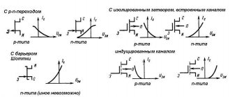
To begin with, it must be said that bipolar transistors can be of two different structures. This is the structure of PNP and NPN. While we won't get into the theory, just remember that a bipolar transistor can be either a PNP or an NPN structure.
On circuit diagrams, bipolar transistors are designated like this.
As you can see, the figure shows two conventional graphic symbols. If the arrow inside the circle is directed towards the central line, then this is a transistor with a PNP structure. If the arrow is directed outward, then it has an NPN structure.
A little advice.
In order not to remember the symbol and immediately determine the type of conductivity (pnp or npn) of a bipolar transistor, you can use the following analogy.
First, look where the arrow points in the conventional image. Next, imagine that we are going in the direction of the arrow, and if we hit a “wall” - a vertical line - then it means “There is no ”! “ No ” means p- n -p (P- N -P).
Well, if we walk and don’t run into a “wall,” then the diagram shows a transistor of the npn structure. A similar analogy can be used in relation to field-effect transistors when determining the type of channel (n or p). Read about the designation of different field-effect transistors in the diagram here.
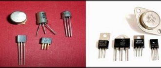
Typically, a discrete, that is, a separate transistor has three outputs. Previously, it was even called a semiconductor triode. Sometimes it may have four terminals, but the fourth is used to connect the metal case to the common wire. It is shielding and is not connected to other pins. Also, one of the terminals, usually a collector (discussed later), may have the shape of a flange for attachment to a cooling radiator or be part of a metal case.
Take a look. The photo shows various transistors of Soviet production, as well as the early 90s.
But this is a modern import.
Each of the terminals of the transistor has its own purpose and name: base, emitter and collector. Usually these names are abbreviated and written simply B ( Base ), E ( Emitter ), K ( Collector ). On foreign diagrams, the collector output is marked with the letter C , this is from the word Collector - “collector” (the verb Collect - “to collect”). The output of the base is marked as B , from the word Base (from the English Base - “main”). This is the control electrode. Well, the emitter pin is designated by the letter E , from the word Emitter - “emitter” or “source of emissions”. In this case, the emitter serves as a source of electrons, a supplier, so to speak.
The terminals of the transistors must be soldered into the electronic circuit, strictly observing the pinout. That is, the collector output is soldered exactly to that part of the circuit where it should be connected. You cannot solder the collector or emitter output instead of the base output. Otherwise the scheme will not work.
How do you find out where on the circuit diagram of a transistor the collector is and where the emitter is? It's simple. The pin with the arrow is always the emitter. The one that is drawn perpendicular (at an angle of 90 0) to the central line is the output of the base. And the one that remains is the collector.
Also on circuit diagrams, the transistor is marked with the symbol VT or Q. In old Soviet books on electronics you can find a designation in the form of the letter V or T. Next, the serial number of the transistor in the circuit is indicated, for example, Q505 or VT33. It is worth considering that the letters VT and Q denote not only bipolar transistors, but also field-effect transistors.
Next, we will learn how to find transistors on the printed circuit board of an electronic device.
The main differences between the two types of bipolar transistors
The main difference between them is that holes are the main current carriers for PNP transistors, NPN transistors have electrons in this capacity. Therefore, the polarities of the voltages supplying the transistor are reversed, and its input current flows from the base. In contrast, with an NPN transistor, the base current flows into it, as shown below in the circuit diagram for connecting both types of devices with a common base and a common emitter.
The operating principle of a PNP-type transistor is based on the use of a small (like the NPN-type) base current and a negative (unlike the NPN-type) base bias voltage to control a much larger emitter-collector current. In other words, for a PNP transistor, the emitter is more positive with respect to the base and also with respect to the collector.
Indeed, it can be seen that the collector current IC (in the case of an NPN transistor) flows from the positive terminal of battery B2, passes through the collector terminal, penetrates into it and must then exit through the base terminal to return to the negative terminal of the battery. In the same way, looking at the emitter circuit, you can see how its current from the positive terminal of battery B1 enters the transistor through the base terminal and then penetrates into the emitter.
The base terminal thus carries both the collector current IC and the emitter current IE. Since they circulate in opposite directions along their circuits, the resulting base current is equal to their difference and is very small, since IC is slightly smaller than IE. But since the latter is still larger, the direction of flow of the difference current (base current) coincides with IE, and therefore a PNP-type bipolar transistor has a current flowing out of the base, and an NPN-type one has an inflowing current.
Anatomy of marking
There will be no mistakes if you understand the basic anatomy of semiconductor component markings. Of course, this will not solve all problems, but you must know the three components of marking.
Usually the labeling has a prefix that provides some basic information about the device, but the encoding methods used are very simple and never tell you about a specific device. However, when purchasing components, the prefix can be (and quite often is) very important.
The second part is the main one (like the serial number of the product) and has three or four digits.
The third part, the suffix , provides some additional information about the device, but it is not always present, especially for transistors and diodes. It is only needed if there are two or more different versions of the device .
Again, this is important when purchasing components, and you can easily end up with the wrong version if the device has the wrong suffix. There are many examples of identical devices that have different suffixes.
Middle management
The main part is the simplest part of marking semiconductor elements. The first device of this type to be registered may be numbered “0001”, the next one “0002”, etc.
In practice, this doesn't quite work that way, and some transistor manufacturers start labeling their products with "100" rather than "001". But that doesn't matter.
A significant disadvantage of this marking method is the presence of more semiconductor devices than available numbers (3 or 4 digits).
For example, a device labeled "555" could be a popular timer integrated circuit (IC), a transistor with a European number type, and perhaps something else, such as another type of integrated circuit or optical device.
Thus, basic numeric markings are important but are not sufficient on their own to accurately identify an item.
To select the appropriate element, you must pay attention to other parts of the marking.
Application of transistors in life
Transistors are used in many technical devices. The most striking examples:
- Amplifier circuits.
- Signal generators.
- Electronic keys.
In all communication devices, signal amplification is necessary. First, electrical signals naturally attenuate. Secondly, it often happens that the amplitude of one of the signal parameters is not enough for the device to operate correctly. Information is transmitted using electrical signals. In order for delivery to be guaranteed and the quality of information to be high, we need to strengthen the signals .
Transistors can influence not only the amplitude, but also the shape of an electrical signal. Depending on the required shape of the generated signal, the appropriate type of semiconductor device will be installed in the generator.
Electronic keys are needed to control the current strength in the circuit. These switches contain many transistors. Electronic keys are one of the most important elements of circuits. They are the basis for computers, televisions and other electrical appliances, which are indispensable in modern life.
Start over
The first part of the marking ( prefix ) serves two functions, and for European manufacturers this part of the marking gives some basic information about the type of device. It is somewhat similar and takes its origins from the marking of vacuum tubes, but in relation to solid-state devices, the first letter indicates the type of semiconductor material used or the type of integrated circuit:
| First character | Item type |
| A | Germanium |
| B | Silicon |
| C | Gallium arsenide |
| F | Integrated logic circuit |
| R | Photocell |
| S | Digital integrated circuit |
| T | Linear integrated circuit |
The second letter indicates the device type, as in Table 2.
| Second character | Device type |
| A | Signal diode |
| B | Varicap |
| C | Low power transistor for audio |
| D | Powerful transistor for audio |
| E | Tunnel diode |
| F | Low-power high-frequency transistor |
| L | Powerful high frequency transistor |
| P | Phototransistor |
| S | Transistor for key circuits |
| T | Thyristor |
| Y | Filter |
| Z | Zener diode |
Note that elements for industrial applications are marked with three letters.
For example, the BC550 is a small silicon transistor for audio or other low-frequency applications, while the BF181 is a low-power silicon transistor for RF use.
PRO-ELECTRON (system developed in Europe)
The marking of devices from European manufacturers is somewhat different. The code with which the foreign transistor is marked is a combination of the symbol:
- The symbol number one indicates the material from which the device is made: A – germanium, B – silicon, C – gallium arsenide, R – cadmium sulfide;
- The second symbol indicates the type of transistor: C – low-power device with low frequency; D – powerful element with low frequency; F – low power device with a high frequency level; G – two or more elements are present in one case at the same time; L – device with high power and frequency; S – low-power device with switching function; U – high power switch transistor;
- The third character indicates the product series number: general use products are marked with numbers from 100 to 999; in the case when a letter is written before the digital value, this indicates that this part is manufactured for use in industry or specialized use.
Moreover, the general encoding is sometimes supplemented with a modification symbol. Only the manufacturer himself can determine it.
One less
Simple semiconductors from American manufacturers are marked according to the JEDEC (Joint Electron Devices Engineering Council) system and have a prefix consisting of a number followed by the letter N. The number is one less than the number of terminals the device has, which in practice means 1 for diodes and zener diodes (i.e. two terminals), "2" for regular transistors, and "3" or more for special devices such as dual-gate MOSFETs. -transistors and so on.
So the 1N4148 is a device that has two terminals, which usually means a diode. This is actually a small diode, but this information is not displayed in the JEDEC type markings, which turn out to be less informative than the European Pro Electron.
the Japanese marking is not often found , but the first digit in it is again a number that is one less than the number of pins of the element. This is followed by two letters that identify the general type of device:
| Marking | Device type |
| S.A. | High frequency PNP transistor |
| S.B. | High frequency NPN transistor |
| S.C. | PNP transistor for audio |
| SD | NPN transistor for audio |
| S.E. | Diode |
| S.J. | P-channel field effect transistor (including MOSFET) |
| S.K. | N-field effect transistor (including MOSFET) |
| S.R. | Filter |
As you can see, for conventional transistor types the first two digits are always "2S" and are perhaps a bit useless, so these two digits are often omitted when labeling elements.
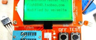
Checking bipolar types
Below is a diagram for checking npn, pnp transistors with a tester, after which we will describe the procedure point by point.
The bipolar transistor is equipped with pn lines - conventionally, these are diodes, or rather, 2 of them located oppositely, the point of their intersection is the “base”.
One conditional diode is designed with base/collector contacts, the other with base/emitter contacts. For analysis, just look at the contrast. (directly and back) of the indicated areas: if there are no problems there, then the part is without flaws.
Do-it-yourself testing without soldering a bipolar pnp, npn transistor involves testing 3 combinations of legs:
pnp option
Structures (types) are shown by the arrow emitting. section: pnp/npn (to/from the base). Let's start by checking the first option. We open the PNP part by applying negative voltage to the base. On the multimeter, we set the selector to measure Ohms to o; it is also possible to set it to “continuity”.
The vein “−” (black) is on the base leg. Plus (red) - alternately to collect., emitter. If the areas are not damaged, they will display about 500–1200 Ohms.
Next we will describe how to ring the reverse resistance: “+” - to the base, “−” - to the call. and emits. High resistance should be displayed. on both pn sites. We now have “1”, that is, for the frame set to “2000” the value exceeds 2000. This means that there are 2 transitions without breaks, the product is in good working order.
It will be interesting➡ Inductive reactance
Similarly, as described, you can test the transistor for serviceability without removing it from the circuit. Less commonly, there are assemblies where substantial shunting is applied to the transitions, for example, with resistors. Then, if too low resistance is displayed, the part will need to be desoldered.
npn structure
Npn elements are checked in the same way, only the “+” probe goes to the base from the tester.
Symptoms of a problem
If the resistance (direct and reverse) of one of the sections (pn) tends to infinity, that is, at o and above on the display “1”, which means that this section has a break, the transistor is unusable. If “0” means the product is also flawed, the area is broken. Direct cont. there should be 500–1200 ohms.
Manufacturer
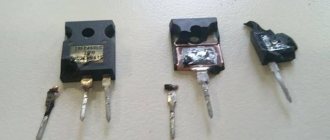
Most electronic components are marked according to the standard methods listed. But there are also exceptions. (Fig. 1).
Here the TIP prefix of this power transistor indicates that it is a plastic packaged power transistor from Texas Instruments. However, the manufacturer put the MOSPEC logo on the front, so the prefix became the second element of the marking.
This often occurs in the marking of integrated circuits, where the manufacturer adds its own coding to the standard type marking.
Fig.2. This integrated circuit has the designation "LM" as a prefix, indicating that it is a National Semiconductor product.
As a few examples: the prefixes "CA" and "MC" are used by KCA and Motorola, respectively. Due to the fact that the same element can be produced by different manufacturers and labeled differently, difficulties arise with identifying the elements.
Of course, the presence of several manufacturers on the market gives rise to competition, which, as a consequence, reduces prices for radioelements. This is good for us. On the other hand, each manufacturer adds something different to the labeling of elements, thereby making it difficult for us to identify them.
When browsing through an integrated circuit catalog, it's probably best to ignore the prefix and focus on the other two markings. Moreover, component suppliers often do not guarantee the supply of devices from specific manufacturers. If you order (say) MC1458CP. but they sent you CA1458E. or vice versa, there is no reason to worry. Both ICs are 1458 dual op amps and there is no practical difference between them. The MC1458CP is made by Motorola or Texas Instruments, and the CA1458E is made by RCA.
Marking of the year and month of manufacture of electronic components
According to GOST 25486-82 , in order to indicate the month and year of manufacture of the transistor and other electronic components, letters and numbers are used: the first value is the year, the second value is the month. As for devices manufactured abroad, a four-digit encoding is used to indicate the date of manufacture, where the first two are the year, the next are the model number.
Each year has its own letter:
Year Code
| 1986 | U |
| 1987 | V |
| 1988 | W |
| 1989 | X |
| 1990 | A |
| 1991 | B |
| 1992 | C |
| 1993 | D |
| 1994 | E |
| 1995 | F |
| 1996 | H |
| 1997 | I |
| 1998 | K |
| 1999 | L |
| 2000 | M |
| 2001 | N |
| 2002 | P |
| 2003 | R |
| 2004 | S |
| 2005 | T |
| 2006 | U |
| 2007 | V |
| 2008 | W |
| 2009 | X |
| 2010 | A |
| 2011 | B |
| 2012 | C |
| 2013 | D |
| 2014 | E |
| 2015 | F |
Month marking
Month Code
| January | 1 |
| February | 2 |
| March | 3 |
| April | 4 |
| May | 5 |
| June | 6 |
| July | 7 |
| August | 8 |
| September | 9 |
| October | O |
| November | N |
| December | D |
To indicate the month of issue, not only numbers, but also some letters are used: the months from January to September fully correspond to the numbers, the following ones correspond to the first letters of the name of the month.
Variety of options
Most transistors do not have a suffix in their markings. Where present, the suffix is usually a single letter and indicates a gain or some other parameter. Typically, transistors with a low gain are marked with the letter “A”, transistors with a medium gain with the letter “B” and with a high gain with the letter “C”. Specific values or range are indicated in the datasheet for the element.
Therefore, if the diagram shows a transistor with the suffix “B”, you can safely replace it with a transistor with the suffix “C”. When replaced with an element with the suffix “A”, its amplification may not be enough and the device will refuse to work or will often go into overload.
There are situations (fortunately, quite rare) when the suffix indicates the location of the terminals of the element. For transistors, these are designated "L" or "K". Most transistors have one typical terminal configuration. But if your device does not work for unknown reasons, check if you have any transistors with such suffixes.
With integrated circuits the situation is the opposite. Here, manufacturers often use a suffix to designate the type of housing. And if you ignore the suffix when ordering or specify the wrong one, you risk receiving a chip in a design that will not be compatible with your printed circuit board option.
The situation is complicated by the fact that there are no standards for suffixes and each manufacturer uses its own types of marking. So be extremely careful when ordering microcircuits!
Symbolically - color marking of transistors
A distinctive feature of this marking is the absence of numbers and letters. The type rating of the transistor is indicated on the cut side surface with a special symbol (dots, horizontal, vertical or dotted lines) or a colored geometric figure (circle, semicircle, square, triangle, rhombus, etc.). The group marking refers to one (several) points on the end of the body (KT-26, KTP-4).
The color scheme of the dots indicating the group for this marking does not coincide with the standard color scheme according to GOST 24709-81. It is determined by the manufacturer.
The circle symbol on the side cut of the transistor must be distinguished from the point, which does not have a clear shape, because applied with a brush.
Frequency marking
Some integrated circuits have a suffix that indicates the clock speed of the device. This system is used in conjunction with memory and some other computer chips such as microcontrollers and microprocessors. In most cases, the additional numbers are actually an extension of the main part of the marking, and not a suffix, since the suffix will be present in the marking and, as mentioned above, will most likely indicate the type of case.
Some PIC microcontrollers, for example, have something like "-20" added to the base number type. Additional markings indicate the maximum clock speed (in megahertz) for the chip. You can quite safely use an item with a higher clock speed than what is listed in the parts list. However, faster versions are usually significantly more expensive than slow ones.
Checking the functionality of the field-effect transistor
This type of semiconductor elements is also called mosfet and mosfet components. Figure 4 shows the graphic designation of n- and p-channel field switches in circuit diagrams.
Figure 4. Field-effect transistors (N- and P-channel)
To test these devices, we connect the probes to the multimeter in the same way as when testing bipolar semiconductors, and set the test type to “continuity”. Next, we proceed according to the following algorithm (for an n-channel element):
- We touch the black wire to the “c” pin, and the red wire to the “i” pin. The resistance on the built-in diode will be displayed, remember the reading.
- Now you need to “open” the transition (this will only be possible partially), for this we connect the probe with the red wire to terminal “z”.
- We repeat the measurement carried out in step 1, the reading will change downwards, which indicates a partial “opening” of the field worker.
- Now you need to “close” the component, for this purpose we connect the negative probe (black wire) to the “z” leg.
- We repeat steps 1, the original value will be displayed, therefore, “closing” has occurred, which indicates the serviceability of the component.
To test p-channel elements, the sequence of actions remains the same, with the exception of the polarity of the probes, it must be reversed.
Note that insulated gate bipolar elements (IGBT) are tested in the same way as described above. Figure 5 shows the SC12850 component in this class.
Fig 5. IGBT transistor SC12850
For testing, it is necessary to perform the same steps as for a field-effect semiconductor element, taking into account that the drain and source of the latter will correspond to the collector and emitter.
In some cases, the potential on the multimeter probes may not be enough (for example, to “open” a powerful power transistor); in such a situation, additional power will be needed (12 volts will be enough). It must be connected through a resistance of 1500-2000 Ohms.
And technology.
But, alas, not everything is so simple. Especially with integrated circuits. The 74th series (TTL) of logic integrated circuits was the main one, the progenitor of other series and was originally marked according to the stated rules: prefix-main part-suffix. When marking subsequent, improved series, manufacturers began to deviate from the standard marking - between the prefix “74” and the base number they began to add markings indicating the family of microcircuits:
This marking may indicate the manufacturing technology and, as a result, the speed (frequency), supply voltage and other parameters.
And current!
A similar situation exists with the popularly loved integrated stabilizers L78XX and L79XX. Here two numbers are added to the basic designation, indicating the output voltage of the stabilizers: L7805 - output voltage 5V, L7912 - output voltage -12V.
But in the middle of the number there may be letters that indicate the maximum output current of the stabilizer. Three marking options are possible, as shown in the table:
| Symbol | Maximum current |
| L | 0.1A (100mA) |
| M | 0.5A (500mA) |
| S | 2A |
So a stabilizer marked “78L15” will produce an output voltage of 15V and a maximum current of 100mA.
Be careful when reading manufacturers' catalogs and be careful when ordering electronic components!
The article was prepared based on materials from the magazine “Practical Electronics Every Day”
Author: Robert Penfold
Free translation: Editor-in-Chief of RadioGazeta
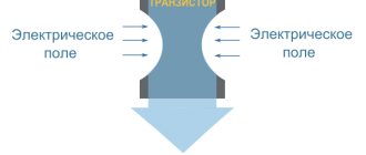
The transistor is one of the most common elements of radio equipment. There are field-effect and bipolar transistors . Field-effect transistors are controlled using an electric field. They have three terminals: source, gate and drain (sometimes body). A bipolar transistor has, respectively, an emitter, a base and a collector (sometimes there is also a body terminal).
Basic classification of transistors
The main classification of transistors is based on material, power, conductivity, frequency...
By power, transistors are divided into low, medium and high power transistors, and by frequency - low-frequency, high-frequency and ultra-high-frequency.
According to the source semiconductor material - germanium and silicon.
Main settings
bipolar and field-effect transistors
UCBO - maximum permissible collector-base voltage;
UCBO I - maximum permissible pulse voltage collector - base;
UCEO - maximum permissible collector-emitter voltage;
U KEO I - maximum permissible collector-emitter pulse voltage;
UKEN - collector-emitter saturation voltage;
USI max - maximum permissible drain-source voltage;
USIO - drain-source voltage when the gate is broken;
UZImax - maximum permissible gate-source voltage;
U ZI OTS - Transistor cut-off voltage at which the drain current reaches a specified low value (for field-effect transistors with a p-n junction and with an insulated gate);
U ZI POR - Threshold voltage of the transistor between the gate and drain, at which the drain current reaches a specified low value (for field-effect transistors with an insulated gate and p-channel);
IK max - maximum permissible direct collector current;
IK max and is the maximum permissible pulse current of the collector;
IC max - maximum permissible constant drain current;
I C start - initial drain current;
I C rest - residual drain current;
IKBO - reverse collector current;
RK max - maximum permissible constant power dissipation of the collector without heat sink;
РКmax t - maximum permissible constant power dissipation of the collector with a heat sink;
RSImax - maximum permissible constant power dissipation drain - source;
H21E - static current transfer coefficient of a bipolar transistor in a circuit with a common emitter;
R SI OTK - drain - source resistance in open state;
S is the slope of the characteristic;
fGR. — cut-off frequency of the current transfer coefficient in a circuit with a common emitter;
KS - noise figure of a bipolar (field-effect) transistor;
Pinout of bipolar and field-effect transistors
Practice of compound transistor operation
In Fig. Figure 3 shows three options for constructing an output stage (emitter follower). When selecting transistors, you should strive for b1~b2 and b3~b4. The difference can be compensated by selecting pairs based on the equality of the ST gain factors b13~b24 (see Table 1).
- Scheme in Fig. 3a has the highest input resistance, but this is the worst of the given circuits: it requires insulation of the flanges of powerful transistors (or separate radiators) and provides the smallest voltage swing, since ~2 V must drop between the bases of the CT, otherwise “step” distortion will appear strongly.
- Scheme in Fig. 3b was inherited from those times when complementary pairs of powerful transistors were not yet produced. The only advantage compared to the previous version is a lower voltage drop of ~1.8 V and a larger swing without distortion.
- Scheme in Fig. 3c clearly demonstrates the advantages of STS: a minimum voltage drops between the ST bases, and powerful transistors can be placed on a common radiator without insulating spacers.
In Fig. Figure 4 shows two parametric stabilizers. The output voltage for the version with STD is:
Since Ube varies depending on temperature and collector current, the output voltage spread of a circuit with STD will be greater, and therefore the option with STS is preferable.
Rice. 3. Options for output emitter followers on ST
Rice. 4. Application of CT as a regulator in a linear stabilizer
Any suitable combination of transistors can be used in linear circuits. The author has encountered Soviet household appliances that used STS in pairs KT315+KT814 and KT3107+KT815 (although /KT361 and KT3102/KT3107 are accepted). As a complementary pair, you can take C945 and A733, often found in old computer power supplies.
For switching electromechanical drives and, especially, in pulse circuits, ready-made CTs with standardized on and off parameters and parasitic capacitances should be used. A typical example is the widespread imported complementary STD of the TIP12x series.