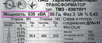
Electronics for everyone
Except transistors
Darlington
assemblies, there is another good way to drive a powerful constant load -
MOSFETs . A field-effect transistor operates like a conventional transistor - a weak signal at the gate controls a powerful flow through the channel. But, unlike bipolar transistors, here the control is not by current, but by voltage .
MOS (in bourgeois MOSFET ) stands for Metal-Oxide-Semiconductor; from this abbreviation the structure of this transistor becomes clear.
If on the fingers, then it has a semiconductor channel that serves as one plate of the capacitor and the second plate is a metal electrode located through a thin layer of silicon oxide, which is a dielectric. When voltage is applied to the gate, this capacitor is charged, and the electric field of the gate pulls charges to the channel, as a result of which mobile charges appear in the channel that can form an electric current and the drain-source resistance drops sharply. The higher the voltage, the more charges and lower the resistance, as a result, the resistance can drop to tiny values - hundredths of an ohm, and if you raise the voltage further, a breakdown of the oxide layer and the Khan transistor will occur. The advantage of such a transistor, compared to a bipolar one, is obvious - voltage must be applied to the gate, but since there is a dielectric, the current will be zero, which means the required power to control this transistor will be negligible; in fact, it consumes only at the moment of switching, when charging is in progress and capacitor discharge.
The disadvantage arises from its capacitive property - the presence of capacitance on the gate requires a large charging current when opening. In theory, equal to infinity on infinitely small periods of time. And if the current is limited by a resistor, then the capacitor will charge slowly - there is no escape from the time constant of the RC circuit.
MOS transistors come in P and N channel. They have the same principle, the only difference is the polarity of the current carriers in the channel. Accordingly, in different directions of the control voltage and inclusion in the circuit. Very often transistors are made in the form of complementary pairs. That is, there are two models with exactly the same characteristics, but one of them is N channel, and the other is P channel. Their markings, as a rule, differ by one digit.
The load is connected to the drain circuit. In general, in theory, it makes no difference to a field-effect transistor what is considered a source and what is a drain - there is no difference between them. But in practice there is, the fact is that to improve the characteristics, the source and drain are made of different sizes and designs, plus, in powerful field devices there is often a reverse diode (it is also called parasitic, because it is formed by itself due to the peculiarities of the technical process production).
My most popular MOS transistors are IRF630 (n channel) and IRF9630 (p channel). At one time I installed about a dozen of each type. Possessing a not very large TO-92 , this transistor can easily pull through itself up to 9A. Its open resistance is only 0.35 Ohm. However, this is a rather old transistor; now there are better things, for example IRF7314 , capable of carrying the same 9A, but at the same time it fits into an SO8 case - the size of a notebook square.
One of the problems of joining MOSFET transistor and a microcontroller (or digital circuit) is that in order to fully open until completely saturated, this transistor needs to drive quite a higher voltage to the gate. Usually this is about 10 volts, and the MK can output a maximum of 5. There are three options:
- Using smaller transistors, build a chain that supplies power from the high-voltage circuit to the gate in order to pump it with high voltage
- use a special driver chip, which itself will generate the required control signal and equalize the levels between the controller and the transistor. Typical examples of drivers are, for example, IR2117.
You just need to remember that there are upper and lower shoulder drivers (or combined, half-bridge). The choice of driver depends on the load connection circuit and the switching transistor. If you pay attention, you will see that N channel transistors are used with the driver in both the upper and lower arms. They just have better characteristics than P channel ones. But here another problem arises. In order to open the N channel transistor in the upper side, it needs to apply a voltage higher than the drain voltage to its gate, and this, in fact, is higher than the supply voltage. To achieve this, a voltage pump is used in the high-side driver. What exactly is the difference between a lower shoulder driver and an upper shoulder driver?
- Use a transistor with a low turn-on voltage. For example, from the IRL630A series or the like. Their opening voltages are tied to logical levels. They do have one drawback - they are sometimes difficult to get. If ordinary powerful field workers are no longer a problem, then those controlled by the logical level are not always the case.
But in general, it is more correct to install a driver, because in addition to the main functions of generating control signals, it also provides current protection, protection against breakdown, overvoltage, as an additional bauble, optimizes the opening speed to the maximum, in general, it does not consume its current in vain.
Choosing a transistor is also not very difficult, especially if you don’t bother with limiting modes. First of all, you should be concerned about the value of the drain current - I Drain or ID; you select a transistor based on the maximum current for your load, preferably with a margin of 10 percent. The next important parameter for you is VGS - Source-Gate saturation voltage or, more simply put, control voltage. Sometimes it is written, but more often you have to look at the charts. You are looking for a graph of the output characteristics Dependence of ID on VDS at different values of VGS . And you figure out what kind of regime you will have.
For example, you need to power the engine at 12 volts, with a current of 8A. You screwed up the driver and only have a 5 volt control signal. The first thing that came to mind after this article was IRF630. The current is suitable with a margin of 9A versus the required 8. But let’s look at the output characteristic:
You see, at 5 volts on the gate and a current of 8A, the voltage drop across the transistor will be about 4.5V. According to Ohm's law, then it turns out that the resistance of this transistor at the moment is 4.5/8 = 0.56 Ohm . Now let’s calculate the power losses - your engine consumes 5A. P=I*U or, if we apply the same Ohm's law, P=I2R . At 8 amperes and 0.56 Ohm the loss will be 35 W. It hurts a lot, don't you think? I also think it’s too much. the IRL630 then .
At 8 amps and 5 volts on the Gate, the voltage across the transistor will be about 3 volts. Which will give us 0.37 Ohm and 23 W losses, which is noticeably less.
If you are going to use PWM on this switch, then you need to inquire about the opening and closing times of the transistor, choose the largest one and, relative to the time, calculate the maximum frequency of which it is capable. This value is called Switch Delay or ton , toff , in general, something like that. Well, the frequency is 1/t. It would also be a good idea to look at the gate capacitance Ciss , based on it, as well as the limiting resistor in the gate circuit, you can calculate the charging time constant of the RC gate circuit and estimate the performance. If the time constant is greater than the PWM period, then the transistor will not open/close, but will hang in some intermediate state, since the voltage at its gate will be integrated by this RC circuit into a constant voltage.
When handling these transistors, take into account the fact that they are not just very afraid of static electricity, but VERY STRONG . It is more than possible to penetrate the shutter with a static charge. So when you buy it, immediately wrap it in foil and don’t take it out until you seal it. First ground yourself to the battery and put on a foil hat :).
And in the process of designing a circuit, remember one more simple rule - under no circumstances should you leave the field gate shutter hanging just like that - otherwise it will eat noise from the air and open on its own. Therefore, it is necessary to install a 10 kilo-ohm resistor from Gate to GND for N channel or +V for P channel, so that the parasitic charge flows off. That seems to be all, next time I’ll write about bridge circuits for controlling engines.
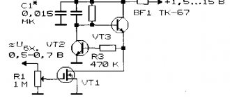
Field effect transistor device
The electronic load on the field-effect transistor is made only on the basis of the comparator, and the thyristor is used of an adjustable type. When assembling, first of all, you should select a capacitor unit, which plays the role of a pulse generator. A total of three filters will be required for modification. The resistor is installed behind the plates. Experts say that the electronic load on the field-effect transistor produces a resistance of 40 Ohms.
If the conductivity increases significantly, then a capacitive capacitor is installed. It is recommended to use the transceiver itself with two contacts. The relay is installed as standard with a regulator. The rated voltage for loads of this type is no more than 400 W. Experts say that the plate should be fixed behind the resistor. If we consider a high-frequency model for 300 V power supplies, then a modulator will be required of the wave type. In this case, a tetrode is installed behind the thyristor.
Devices based on KTC8550
Loads based on transistor data are highly valued among professionals. The models are great for testing low-power units. The permissible overload indicator is usually 5 A. Models may use different protection systems. When assembling the modification, it is allowed to use binary modulators with a conductivity of 4 μm. Thus, the devices will output a higher frequency at 300 kHz.
If we talk about the disadvantages, it is worth noting that the modifications are not able to work with 10 A power supplies. First of all, problems arise with pulse surges. Overheating of the capacitor will also make itself felt. To solve this problem, expanders are installed on the loads. Triodes are usually used with two plates and an insulator.
ITECH series models
The loads of this series are distinguished by their high conductivity. They have good security. In this case, several transceivers are used. The electronic load for the power supply operates at an average frequency of 200 kHz. The overload in this case is 4 A. Amplifiers in the devices are used with contact adapters. Thyristors are used of phase or code type. Among the models in this series there are programmable modifications. They are well suited for testing computer power supplies. Transceivers can be found with or without expanders.
AMETEK devices
Loads of this brand are distinguished by low conductivity. They are great for 15 A power supplies. Among the models of this company there are many pulse modifications. Their specific overload is not high, but they provide a high pulse generation rate. Experts primarily note the good protection of the elements. They use several filters. They cope with phase interference that distorts signals.
If we consider high-frequency models, they have several thyristors. It is also worth noting that modifications based on wired comparators are available on the market. Based on the usual load of this brand, you can assemble an excellent device for different power supplies. The models have excellent stabilizers and very sensitive transistors.
Models for 10 A units
The electronic load for a 10 A power supply is collected using an expansion thyristor. Transistors are quite often used at 5 pF, which have low conductivity. It is also worth noting that experts do not recommend using linear analogues. They have low sensitivity. They greatly increase the dissipation coefficient. Contactors are used to connect to the block. Modulators are quite often used with adapters.
If we consider the circuit on a capacitor block, then their frequency is on average 400 kHz. In this case, sensitivity may change. Contactors are quite often fixed behind the modulator. Stabilizers should be used on two plates. It is also worth noting that to assemble the modification you will need a pole resistor. It greatly helps to increase the speed of impulse generation.
Device diagram for 20 A units
The electronic load (circuit shown below) for 20 A units is based on binary resistors. They maintain stable high conductivity. The sensitivity is approximately 6 mV. Some modifications are distinguished by a high overload parameter. Relays in models are used on wave transistors. Comparators are used to solve conversion problems. Expanders are often found in the phase type. And they may have several adapters. If necessary, the device can be assembled independently. For this, a capacitor unit is used.
The rated voltage of homemade loads starts from 300 W, and the average frequency is 400 kHz. Experts do not recommend using transient comparators. Regulators are used with plates. To install the comparator you will need an insulator. If we consider loads on two thyristors, then filters are used there. On average, the module capacitance is 3 pF. The dispersion rate for homemade models starts at 50%. When assembling the device, special attention should be paid to the adapter for connecting to the power supply. Contactors are of the pole type. They must withstand heavy overloads and not overheat.
Devices for 15 A units
The most common loads are for 15 A units. They use open resistors. In this case, transceivers are used with different polarities. In addition, they differ in sensitivity. On average, the voltage of the devices is 320 V. The models differ in conductivity. For the purpose of self-assembly, comparators are used on regulators. Before installing them, stabilizers are attached.
Experts say that expanders can only be installed through the lining. The conductivity at the input must be no more than 6 microns. When installing the regulator, the comparator is thoroughly cleaned. If you assemble a simple model, then the modulator can be used of the inverter type. This will greatly increase the dispersion coefficient. The threshold voltage is on average 200 V. The permissible power parameter is no more than 240 W. It is also worth noting that different types of filters are used for the load. In this case, much depends on the conductivity of the comparator.
Features of Sorensen series devices
The standard electronic load of this series includes a thyristor and a linear comparator. Many models are manufactured with pole filters that are capable of operating at high frequencies. It is also worth noting that laboratory modifications are available on the market. They have a fairly low dissipation coefficient. Models quite often used are switched type. The average overload indicator is 20 A. Protection systems are used in different classes. There are impulse models on store shelves. They are well suited for testing computer power supplies. Expanders in devices are used with covers.
How does he work
A field-effect transistor includes several components - a source (a source of charge carrier like an emitter on a bipolar element), a drain (a charge receiver like a collector) and a gate (a control electrode like a grid in lamps or a base). The work of the first two is obvious and consists in generating and receiving electric charge carriers, including electrons and holes. The gate is needed primarily to control the electric current that flows through the PT. That is, it turns out to be a classic triode with a cathode, anode and a control-type electrode.
When voltage is applied to the gate, an electric field is generated that changes the width of certain junctions and affects the parameter of the electric current flowing from source to drain. If there is no control voltage, then nothing will impede the flow of charge carriers in the form of electrons. When the control voltage increases, the channel through which electrons or holes move, on the contrary, decreases, and when a certain limit is reached, it closes completely, and the field-effect transistor enters the so-called cutoff mode. It is this characteristic of PTs that makes it possible to use them as keys.
Connecting a load to an electrotransistor to open it
The current amplification properties of this radio component are due to the fact that the strong electric current that flows from source to drain repeats all the dynamic characteristics of the voltage applied to the gate. In other words, from the output of this amplifier a signal is taken that is absolutely the same in shape as at the control electrode, only stronger.
The structure of the PT (unipolar transistor) is slightly different from the bipolar one. Namely, because the electricity in it crosses certain transition zones. Electric charges move through a regulation area called a gate. Its throughput is regulated by the voltage parameter.
Types of field-effect transistors with markings
Important! The space of the transistor zones under the influence of an electric field decreases and increases. Based on this, the number of charge carriers changes - from their complete absence to an excess.