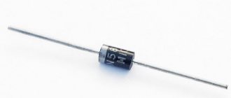
A diode is one of the types of devices designed on a semiconductor basis. It has one pn junction, as well as anode and cathode terminals. In most cases, it is designed for modulation, rectification, conversion and other actions with incoming electrical signals.
Principle of operation:
- An electric current acts on the cathode, the heater begins to glow, and the electrode begins to emit electrons.
- An electric field is formed between the two electrodes
- If the anode has a positive potential , then it begins to attract electrons to itself, and the resulting field is a catalyst for this process. In this case, an emission current is generated.
- Between the electrodes, a negative spatial charge is formed, which can interfere with the movement of electrons. This happens if the anode potential is too weak. In this case, some of the electrons are unable to overcome the influence of the negative charge, and they begin to move in the opposite direction, returning to the cathode again.
- All electrons that reach the anode and do not return to the cathode determine the parameters of the cathode current. Therefore, this indicator directly depends on the positive anode potential.
- The flow of all electrons that were able to get to the anode is called the anode current, the indicators of which in the diode always correspond to the parameters of the cathode current. Sometimes both indicators can be zero; this happens in situations where the anode has a negative charge. In this case, the field that arises between the electrodes does not accelerate the particles, but, on the contrary, slows them down and returns them to the cathode. The diode in this case remains in a locked state, which leads to an open circuit.
Device
Below is a detailed description of the diode structure; studying this information is necessary for further understanding of the principles of operation of these elements:
- The housing is a vacuum cylinder that can be made of glass, metal or durable ceramic varieties of material.
- inside the cylinder . The first is a heated cathode, which is designed to ensure the process of electron emission. The simplest cathode in design is a filament with a small diameter, which heats up during operation, but today indirectly heated electrodes are more common. They are cylinders made of metal and have a special active layer capable of emitting electrons.
- Inside the indirectly heated there is a specific element - a wire that glows under the influence of electric current, it is called a heater.
- The second electrode is the anode, it is needed to receive the electrons that were released by the cathode. To do this, it must have a potential that is positive relative to the second electrode. In most cases, the anode is also cylindrical.
- Both electrodes of vacuum devices are completely identical to the emitter and base of the semiconductor variety of elements.
- Silicon or germanium is most often used to make a diode crystal One of its parts is p-type electrically conductive and has a deficiency of electrons, which is formed by an artificial method. The opposite side of the crystal also has conductivity, but it is n-type and has an excess of electrons. There is a boundary between the two regions, which is called a pn junction.
Such features of the internal structure give diodes their main property - the ability to conduct electric current in only one direction.
Purpose
Below are the main areas of application of diodes, from which their main purpose becomes clear:
- Diode bridges are 4, 6 or 12 diodes connected to each other, their number depends on the type of circuit, which can be single-phase, three-phase half-bridge or three-phase full-bridge. They perform the functions of rectifiers; this option is most often used in automobile generators, since the introduction of such bridges, as well as the use of brush-collector units with them, has made it possible to significantly reduce the size of this device and increase its reliability. If the connection is made in series and in one direction, this increases the minimum voltage required to unlock the entire diode bridge.
- Diode detectors are obtained by combining these devices with capacitors. This is necessary so that it is possible to isolate low-frequency modulation from various modulated signals, including the amplitude-modulated variety of the radio signal. Such detectors are part of the design of many household appliances, such as televisions or radios.
- Ensuring protection of consumers from incorrect polarity when switching on circuit inputs from occurring overloads or switches from breakdown by electromotive force that occurs during self-induction, which occurs when the inductive load is turned off. To ensure the safety of circuits from overloads that occur, a chain is used consisting of several diodes connected to the supply buses in the reverse direction. In this case, the input to which protection is provided must be connected to the middle of this chain. During normal operation of the circuit, all diodes are in a closed state, but if they have detected that the input potential has gone beyond the permissible voltage limits, one of the protective elements is activated. Due to this, this permissible potential is limited within the permissible supply voltage in combination with a direct drop in the voltage on the protective device.
- Switches based on diodes are used to switch high-frequency signals. Such a system is controlled using direct electric current, high-frequency separation and the supply of a control signal, which occurs due to inductance and capacitors.
- Creation of diode spark protection . Shunt-diode barriers are used, which provide safety by limiting the voltage in the corresponding electrical circuit. In combination with them, current-limiting resistors are used, which are necessary to limit the electric current passing through the network and increase the degree of protection.
Read also: Band saw blade speed
IGBT dynamic parameters
The behavior of IGBTs in pulsed modes is determined by their structure, the size of internal capacitors and resistances, as well as load parameters. Unlike an ideal switch, dynamic control of an IGBT requires a certain power, which is associated with the need to recharge the input capacitances of an isolated MOS gate. In addition, the switching process is significantly influenced by the distributed inductances of the power terminals inside the module and the DC link buses of the converter. Their presence in combination with parasitic capacitances of power crystals and connecting circuits leads to the appearance of switching overvoltages and oscillations.
The dependence of the IGBT pulse characteristics on the size of the internal capacitors and resistances can be explained as follows. When the transistor is turned off, the reverse capacitance value is CGC
small and approximately equal to
CCE
.
When turned on, the CGC
increases rapidly until the gate-to-emitter voltage
VGE
equals
VCE
, due to the inversion of the saturable layer underneath the gate region.
The technical documentation for IGBTs usually gives the values of the input and output capacitors Cies
,
Cres
,
Coes
in the off state (Table 2).
The value of this data for calculating impulse characteristics is small, since when the transistor is switched, the values of Cies
and
Cres
change within very wide limits. Much more useful for calculations is the graph relating charge and gate voltage (Fig. 20a).
Rice. 20. a) Gate charge characteristics;
b) small-signal IGBT capacitors Table 2.
Definition of small-signal IGBT capacitances
| Capacity Description | Meaning |
| Input Cies | Cies = CGE+CGC |
| Reverse (Miller) Cres | Cres = CGC |
| Weekend Coes | Coes = CCG + CCE |
In Fig. Figure 19 shows the process of “hard” switching of an IGBT to a resistive-inductive load, ensuring current continuity, since the load time constant L/R is much greater than the period of the operating frequency (1/ fsw
).
This mode of operation is the most indicative for a qualitative assessment of the dynamic properties of the power switch. In Fig. 19a shows typical collector current and voltage curves depending on the control signal VGE
;
It also shows the operating characteristic of switching on and off in the form of a graph IC
=
f
(
VCE
). These graphs, with minor modifications, are also valid for MOSFET switches.
Rice. 19. Typical characteristics of “hard” switching MOSFET and IGBT (resistive-inductive load): a) current and voltage; b) on/off operating characteristic and measurement circuit
During the “hard” switching process, the transistor is exposed to simultaneously high current and voltage values for a short time, since, thanks to the presence of the opposed diode, the current in the inductance is not interrupted when the IGBT is turned off:
- When the transistor is turned on, it takes on the entire load current Iload
, and the full voltage is applied to the closed diode.
The collector current IC
reaches the value
Iload
before the voltage
VCE
drops to the saturation level
VCE(sat)
. - When the transistor is turned off, the opposed diode can take on the load current only after transitioning to the conducting state. To do this, the collector-emitter voltage must exceed the level of the switched signal before the collector current drops below the cutoff level.
Unlike thyristors, IGBTs are capable of operating in hard mode without the use of snubbers due to the so-called “dynamic transition” formed in the drift zone during switching. The transistor, however, dissipates a lot of energy:
Using a passive snubber circuit, the performance characteristic (Fig. 19b) can be shifted closer to the coordinate axes. Switching losses then pass from the transistor to the snubber, which in most cases reduces the efficiency of the entire system. Since the maximum possible operating area depends not only on current/voltage/frequency, but also on factors associated with the imperfection of the transistor, the actual safe operating area (SOA) is given in the technical specifications for various operating conditions.
As shown in Fig. 19, when IGBT is turned on, voltage VCE
within 10 ns it decreases to a level equivalent to a drop in
the n
-drift region.
Then the n
-band is transferred by positively charged carriers from
the p
-collector;
After a period of time ranging from a few nanoseconds to a few microseconds, the dynamic saturation voltage VCE(sat)dyn
drops to the static saturation level
VCE(sat)
.
Enable IGBT
- 0– t1
(transistor blocked).
When the VGE
a current begins to flow through the gate circuit, charging the capacitor CGE to the value
QG1
.
VGE
level increases linearly with a time constant determined by the input capacitance of the IGBT and the gate resistance
RG
, and until it reaches the threshold value
VGE(sat)
, the transistor is turned off and there is no collector current.
- t1
–
t2
(collector current rise).
After reaching the threshold level (moment t1
)
IC
starts to rise.
At the same time, the signal VGE
associated with the collector current in the active working area of the IGBT in accordance with the expression
IC
=
gfs
×
VGE
(
gfs
- conductivity) increases to the value
VGE
=
IC
/
gfs
(time
t2
).
Since the box diode continues to maintain current at point t2
, the collector voltage
VCE
decreases slightly.
The gate charge in this case reaches the value QG2
.
During a given time interval, the main losses are generated in the IGBT because as long as the magnitude of IC
is less than the load current
IL
, a certain portion
of IL
continues to flow through the opposed diode.
This is why the signal at the collector cannot drop noticeably below the VCC
.
The difference between VCC
and
VCE
, marked in Fig. 19, is mainly caused by dynamic voltage drops on the parasitic inductances of the switched circuits.
- t2
–
t3
(the transistor is fully turned on and is in the active working area, flat section of the characteristic).
When the box diode turns off, the collector voltage drops to saturation level VCE(sat)
, this happens by time
t3
.
In the interval t2
–
t3,
the collector current and gate voltage are still coupled through the conductance
gfs
, and the value of
VCE
remains almost unchanged.
The decline in VCE
creates a compensating current
iG
, charging the Miller capacitance
CCG
to the level (
QG3
–
QG2
), the gate charge at time
t3
is
QG3
.
After the entire load current IL
passes to the transistor, blocking of the opposed diode begins.
However, due to the presence of the reverse recovery effect, the collector current of the IGBT initially increases sharply to the value ( IL
+
IRRM
), after which, as the reduction charge is absorbed,
Qrr
drops to the static level
IL
.
- t3
–
t4
(saturation region).
By time t3
the transistor is fully open, its operating point has passed the active region and reached the saturation limit, the
VGE
and
IC
are no longer related to each other via
gfs
.
The gate voltage continues to increase to the level of the control signal VGG
, and the gate charge increases accordingly, which at this point in time is (
QGtot
–
QG3
).
The collector-emitter voltage cannot immediately reach the saturation level VCE(sat)
;
depending on the value of VG
and
IC
, this occurs within a few hundred nanoseconds.
This so-called "dynamic saturation" phase VCE(sat)dyn
=
f
(
t
) represents the period of time required for minority carriers to occupy the wide
n
-region of the IGBT. This process is also called “conductance modulation.”
Switching off the IGBT
When the IGBT is turned off, all processes occur in reverse order: the gate is fully charged QGtot
must be dissipated by applying a negative control voltage.
The resulting turn-off current discharges the internal capacitances of the transistor to a level at which the influence of charge carriers in the channel region practically disappears, from which point the collector current begins to sharply decline. However, after the emitter current stops due to injection into the collector region of the IGBT, a large number of p
-charge carriers are generated, which continue to be present in
the n
-drift zone.
Now they must recombine or disappear due to back injection, which leads to the appearance of a so-called “tail” residual current. Since it completely drops only a few microseconds after the collector voltage begins to rise, its shape and duration mainly determine the level of turn-off losses Eoff
.
The collector voltage spike shown in Figure 19 is caused by a current interruption in the distributed inductance LS
power circuit.
Its amplitude is proportional to dif
/
dt
and the value of LS. The presence of parasitic components, inevitably present in real-life applications, also leads to distortion of the VGE gate drive signal, which is most pronounced in the “hard” switching mode. The larger the size of these elements, the higher the level of distortion and the more complex the analysis of the dynamic characteristics of the power switch.
Direct diode connection
The pn junction of the diode can be affected by voltage supplied from external sources. Indicators such as magnitude and polarity will affect its behavior and the electrical current conducted through it.
Below we consider in detail the option in which the positive pole is connected to the p-type region, and the negative pole to the n-type region. In this case, direct switching will occur:
- Under the influence of voltage from an external source, an electric field will be formed in the pn junction, and its direction will be opposite to the internal diffusion field.
- The field voltage will decrease significantly, which will cause a sharp narrowing of the blocking layer.
- Under the influence of these processes, a significant number of electrons will be able to freely move from the p-region to the n-region, as well as in the opposite direction.
- The drift current indicators during this process remain the same, since they directly depend only on the number of minority charged carriers located in the pn junction region.
- Electrons have an increased level of diffusion, which leads to the injection of minority carriers. In other words, in the n-region there will be an increase in the number of holes, and in the p-region an increased concentration of electrons will be recorded.
- The lack of equilibrium and an increased number of minority carriers causes them to go deep into the semiconductor and mix with its structure, which ultimately leads to the destruction of its electrical neutrality properties.
- In this case, the semiconductor
Structure
The properties of IGBTs are largely determined by the parasitic elements present in the transistor structure. The accumulation of charge and its subsequent resorption lead to the appearance of switching losses, the creation of a memory effect and the appearance of the so-called “tail” current when turned off. To better understand the processes occurring and possible failure mechanisms, consider the equivalent IGBT electrical circuit (Fig. 17).
Rice. 17. IGBT cell (NPT structure with a planar gate): a) parasitic elements of the structure; b) equivalent electrical circuit with parasitic elements
A description of the physical nature of the parasitic capacitors and resistors shown in the figure is given in Table 1.
Table 1.
Parasitic elements of the IGBT structure
| Symbol | Name | Physical Description |
| C.G.E. | Gate-emitter capacitance | Overlapping metallization of the gate-source region; depends on the gate voltage, does not depend on the collector-emitter voltage |
| C.C.E. | Collector-emitter capacitance | Capacitance of the transition between the n—-drift region and the p-well |
| C.G.C. | Gate-collector container | Miller capacitance is formed by overlapping the gate area and the drift zone n- |
| RG | Internal gate resistor | Polysilicon gate resistor; As a rule, in modules with parallel connection of chips, additional resistance is required to suppress equalizing currents and corresponding oscillations between chips |
| R.D. | Drift resistance | n-region resistance (PNP transistor base resistance) |
| RW | Transverse resistance in the p-pocket area | Base-emitter resistance of a parasitic NPN bipolar transistor |
In addition to internal resistors and capacitors, the equivalent circuit diagram of an IGBT shows an “ideal MOSFET”, an NPN transistor in the gate region ( n
+-emitter region (emitter) /
p
+ -pocket (base) /
n
- drift region with a side resistor
p
+ -pocket under the emitters as a base-emitter resistance RW) and a PNP transistor (
p
+ in the emitter /
n
- drift region - base /
p
+ - pocket - collector), forming, in combination with NPN, a parasitic thyristor structure. This thyristor can latch on when the following condition is met:
where αnpn, αpnp = αТ×gЕ - current amplification of transistors in the base circuits; M
- gain; αТ—base transfer coefficient; γE is the emitter efficiency.
Latching leads to loss of controllability of the IGBT and its failure; this condition must be eliminated in all static and dynamic modes through proper design of the structure, correct selection of gate resistors and snubber circuits. As a rule, the opening of a parasitic thyristor occurs at critical switching speeds (dynamic latch-up due to an increase in hole current relative to the nominal level) or when the critical current density value is exceeded, which decreases with increasing chip temperature.
Each new generation of switches has a higher resistance to latch-up, the main reason for which in modern IGBTs is the multiple excess of the rated current density when turned off.
One of the technological ways to suppress the parasitic trigger structure is to reduce the base-emitter resistance RW
NPN subtransistor by highly doping
the p
+ pocket under
the n
-emitters and shortening the length of
the n
-emitter so that the threshold voltage of the base-emitter junction of the NPN transistor is not reached under all operating conditions. In addition, the hole current (NPN base current) is kept at a minimum level by reducing the current transfer ratio of the PNP transistor. Note that in any case, a compromise has to be found between dynamic characteristics and reliability on the one hand, and conductivity parameters on the other.
Diode reverse connection
Now we will consider another method of switching on, during which the polarity of the external source from which the voltage is transmitted changes:
- The main difference from direct connection is that the created electric field will have a direction that completely coincides with the direction of the internal diffusion field. Accordingly, the barrier layer will no longer narrow, but, on the contrary, expand.
- The field located in the pn junction will have an accelerating effect on a number of minority charge carriers, for this reason, the drift current indicators will remain unchanged. It will determine the parameters of the resulting current that passes through the pn junction.
- As the reverse voltage , the electric current flowing through the junction will tend to reach its maximum. It has a special name - saturation current.
- In accordance with the exponential law , with a gradual increase in temperature, the saturation current indicators will also increase.
Darlington circuit idea
If one transistor can amplify the current, will using two transistors improve our situation? Yes, that's right, it will improve. All we need to do is combine our transistors into a Darlington circuit, this circuit was developed in 1953 by Sidney Darlington.
Approximate connection of two bipolar transistors in a Darlington circuit
When describing the operation of a Darlington circuit, we assume that the collector current is equal to the emitter current (for simplicity, we omit the base current here). We will also take into account that the circuit uses the same type of bipolar transistors. The principle of operation is as follows: the current supplied to the base of T1 flows from its emitter amplified. Let us denote the current gain of this transistor β T1.
T1 flows from the emitter I BT1 · β T1 and directly affects the base of T2. Transistor T2 is amplified by β T2 - multiple. As a result, current I BT1 · β T1 · β T2 flows through the collector T2. Much more of the current flows through T2, so T1's collector current can be considered negligible.
| As a result, the overall current gain of this system is β D = β T1 · β T2. |
Distribution of currents flowing in a Darlington circuit
When transforming the formulas, we made several simplifications. However, they will have little effect on the result (about one percent). The current gain of transistors fluctuates much more (temperature, manufacturer).
| If you have trouble understanding the diagram above, try drawing it on a piece of paper yourself (step by step). |
Forward and reverse voltage
The voltage that affects the diode is divided according to two criteria:
- Direct voltage is the one at which the diode opens and direct current begins to flow through it, while the resistance of the device is extremely low.
- Reverse voltage is one that has reverse polarity and ensures that the diode closes with reverse current passing through it. At the same time, the resistance indicators of the device begin to increase sharply and significantly.
This leads to an increase in the parameters of the forward current passing through the diode. When this device is closed, virtually the entire voltage is applied to it, for this reason the reverse current passing through the diode is insignificant, and the transition resistance reaches peak parameters.
How do bipolar transistors work?
Let's start with a classic bipolar NPN transistor. It has three conclusions:
- Base (b - base)
- Collector (c - collector)
- Emitter (e - emitter)
When a transistor is turned on, current can flow through it from the collector to the emitter. When it is turned off, no current flows. In the example below, the transistor is turned off. This means that no current can flow through it, so the LED will not light up.
To turn on the transistor, you need to apply a voltage of about 0.7 V to the base relative to the emitter. If you had a 0.7V battery you could connect it between the base and emitter and the transistor would turn on. Since most of us don't have a 0.7V battery, how can we turn on the transistor?
Soldering iron YIHUA 8858
Updated version, power: 600 W, air flow: 240 l/h...
More details
Easily! The base-emitter junction of the transistor acts as a diode. The diode has a forward voltage that it “takes” from the available supply voltage. If you connect a resistor in series, then the rest of the voltage will drop across the resistor. So you will automatically get about 0.7V by adding just one resistor.
This is the same principle used to limit the current through an LED so it doesn't burn out.
If you also add a button, then you can control the transistor and therefore the LED by turning it on and off using the button:
Diode operation and its current-voltage characteristics
The current-voltage characteristic of these devices is understood as a curved line that shows the dependence of the electric current flowing through the pn junction on the volume and polarity of the voltage acting on it.
Such a graph can be described as follows:
- The axis is located vertically: the upper area corresponds to the forward current values, the lower area to the reverse current parameters.
- Horizontal axis: The area on the right is for forward voltage values; area on the left for reverse voltage parameters.
- The direct branch of the current-voltage characteristic reflects the passing electric current through the diode. It is directed upward and runs in close proximity to the vertical axis, since it represents the increase in forward electric current that occurs when the corresponding voltage increases.
- The second (reverse) branch corresponds to and displays the state of the closed electric current, which also passes through the device. Its position is such that it runs virtually parallel to the horizontal axis. The steeper this branch approaches the vertical, the higher the rectifying capabilities of a particular diode.
- According to the graph, it can be observed that after an increase in the forward voltage flowing through the pn junction, a slow increase in the electric current occurs. However, gradually, the curve reaches an area in which a jump is noticeable, after which an accelerated increase in its indicators occurs. This is due to the diode opening and conducting current at forward voltage. For devices made of germanium, this occurs at a voltage of 0.1V to 0.2V (maximum value 1V), and for silicon elements a higher value is required from 0.5V to 0.6V (maximum value 1.5V).
- The indicated increase in current readings can lead to overheating of semiconductor molecules. If the heat removal that occurs due to natural processes and the operation of radiators is less than the level of its release, then the structure of the molecules can be destroyed, and this process will be irreversible. For this reason, it is necessary to limit the forward current parameters to prevent overheating of the semiconductor material. To do this, special resistors are added to the circuit, connected in series with the diodes.
- By examining the reverse branch, you can notice that if the reverse voltage applied to the pn junction begins to increase, then the increase in current parameters is virtually unnoticeable. However, in cases where the voltage reaches parameters exceeding the permissible norms, a sudden jump in the reverse current may occur, which will overheat the semiconductor and contribute to the subsequent breakdown of the pn junction.
Read also: Push-button post for 2 buttons connection diagram
Advantages of the Darlington circuit
Darlington transistors are used in the same way as single bipolar ones. They can be considered as one transistor with changed parameters. The most important feature of this change is the multiplication of the current gains.
Let's return to the example given at the beginning: combining a power transistor with β = 40 with a smaller value of β, we get a gain of 1600. To turn on a load that consumes 5 A, only 3 mA is required - this is the current that most microcontrollers successfully provide.
Read also: What is a bridge?
However, it must be remembered that the transistors in this connection are not evenly loaded: most of the current passes through T2. This means that they do not have to be the same type. For example, T1 could be a low power transistor with a large β, making the resulting gain even higher!
Basic diode faults
Sometimes devices of this type fail, this may occur due to natural depreciation and aging of these elements or for other reasons.
In total, there are 3 main types of common faults:
- Breakdown of the junction leads to the fact that the diode, instead of a semiconductor device, becomes essentially a very ordinary conductor. In this state, it loses its basic properties and begins to pass electric current in absolutely any direction. Such a breakdown is easily detected using a standard multimeter, which starts beeping and shows a low resistance level in the diode.
- When a break occurs, the reverse process occurs - the device generally stops passing electric current in any direction, that is, it essentially becomes an insulator. To accurately determine a break, it is necessary to use testers with high-quality and serviceable probes, otherwise they can sometimes falsely diagnose this malfunction. In alloy semiconductor varieties, such a breakdown is extremely rare.
- Leakage , during which the tightness of the device body is broken, as a result of which it cannot function properly.
Breakdown of pn junction
Such breakdowns occur in situations where the reverse electric current begins to suddenly and sharply increase, this happens due to the fact that the voltage of the corresponding type reaches unacceptable high values.
There are usually several types:
- Thermal breakdowns , which are caused by a sharp increase in temperature and subsequent overheating.
- Electrical breakdowns that occur under the influence of current on a junction.
The graph of the current-voltage characteristic allows you to visually study these processes and the difference between them.
Electrical breakdown
The consequences caused by electrical breakdowns are not irreversible, since they do not destroy the crystal itself. Therefore, with a gradual decrease in voltage, it is possible to restore all the properties and operating parameters of the diode.
At the same time, breakdowns of this type are divided into two types:
- Tunneling breakdowns occur when high voltage passes through narrow junctions, which allows individual electrons to escape through it. They usually occur if semiconductor molecules contain a large number of different impurities. During such a breakdown, the reverse current begins to increase sharply and rapidly, and the corresponding voltage is at a low level.
- Avalanche types of breakdowns are possible due to the influence of strong fields that can accelerate charge carriers to the maximum level, due to which they knock out a number of valence electrons from atoms, which then fly into the conductive region. This phenomenon is avalanche-like in nature, which is why this type of breakdown received its name.