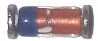
Designation, application and parameters of Schottky diodes
To the large family of semiconductor diodes named after the names of the scientists who discovered the unusual effect, we can add one more.
This is a Schottky diode. German physicist Walter Schottka discovered and studied the so-called barrier effect that occurs with a certain technology for creating a metal-semiconductor transition.
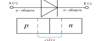
The main feature of a Schottky diode is that, unlike conventional diodes based on a pn junction, it uses a metal-semiconductor junction, which is also called a Schottky barrier. This barrier, just like the semiconductor pn junction, has the property of one-way electrical conductivity and a number of distinctive properties.
The materials used to make Schottky barrier diodes are predominantly silicon (Si) and gallium arsenide (GaAs), as well as metals such as gold, silver, platinum, palladium and tungsten.
In circuit diagrams, a Schottky diode is depicted like this.
As you can see, its image is somewhat different from the designation of a conventional semiconductor diode.
In addition to this designation, in the diagrams you can also find an image of a dual Schottky diode (assembly).
A dual diode is two diodes mounted in one common housing. The terminals of their cathodes or anodes are combined. Therefore, such an assembly, as a rule, has three outputs. Switching power supplies usually use common cathode assemblies.
Since two diodes are placed in the same housing and made in a single technological process, their parameters are very close. Since they are placed in a single housing, their temperature conditions are the same. This increases the reliability and service life of the element.
Schottky diodes have two positive qualities: a very low forward voltage drop (0.2-0.4 volts) across the junction and very high performance.
Unfortunately, such a small voltage drop occurs when the applied voltage is no more than 50-60 volts. As it increases further, the Schottky diode behaves like a regular silicon rectifier diode. The maximum reverse voltage for Schottky usually does not exceed 250 volts, although on sale you can find samples rated at 1.2 kilovolts (VS-10ETS12-M3).
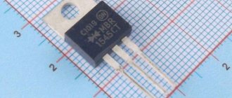
Thus, the dual Schottky diode (Schottky rectifier) 60CPQ150 is designed for a maximum reverse voltage of 150V, and each of the diodes in the assembly is capable of passing 30 amperes in direct connection!
You can also find samples whose half-cycle rectified current can reach a maximum of 400A! An example is the VS-400CNQ045 model.
Very often, in circuit diagrams, the complex graphical representation of the cathode is simply omitted and the Schottky diode is depicted as a regular diode. And the type of element used is indicated in the specification.
The disadvantages of diodes with a Schottky barrier include the fact that even if the reverse voltage is briefly exceeded, they instantly fail and, most importantly, irreversibly. While silicon power valves, after the excess voltage stops, are perfectly self-healing and continue to work. In addition, the reverse current of diodes very much depends on the junction temperature. At a large reverse current, thermal breakdown occurs.
In addition to high speed and, therefore, short recovery time, the positive qualities of Schottky diodes include a small junction (barrier) capacitance, which allows you to increase the operating frequency. This allows them to be used in pulse rectifiers at frequencies of hundreds of kilohertz. A lot of Schottky diodes find their application in integrated microelectronics. Schottky diodes made using nanotechnology are included in integrated circuits, where they bypass transistor junctions to improve performance.
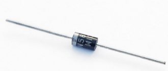
Schottky diodes of the 1N581x series (1N5817, 1N5818, 1N5819) have taken root in amateur radio practice. All of them are designed for a maximum forward current ( IF(AV) ) of 1 ampere and a reverse voltage ( VRRM ) of 20 to 40 volts. The voltage drop ( VF ) across the junction is 0.45 to 0.55 volts. As already mentioned, the forward voltage drop of diodes with a Schottky barrier is very small.
Another fairly well-known element is 1N5822. It is designed for a forward current of 3 amperes and is housed in a DO-201AD housing.
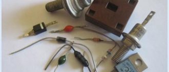
Also on printed circuit boards you can find diodes of the SK12 - SK16 series for surface mounting. They are quite small in size. Despite this, SK12-SK16 can withstand forward current up to 1 ampere at a reverse voltage of 20 - 60 volts. The forward voltage drop is 0.55 volts (for SK12, SK13, SK14) and 0.7 volts (for SK15, SK16). Also in practice you can find diodes of the SK32 - SK310 series, for example, SK36 , which is designed for a forward current of 3 amperes.
Application of Schottky diodes in power supplies.
Schottky diodes are actively used in computer power supplies and switching voltage stabilizers. Among the low-voltage supply voltages, the highest current (tens of amperes) are +3.3 volts and +5.0 volts. It is in these secondary power supplies that Schottky barrier diodes are used. Most often, three-terminal assemblies with a common cathode are used. It is the use of assemblies that can be considered a sign of a high-quality and technologically advanced power supply.
Failure of Schottky diodes is one of the most common faults in switching power supplies. It can have two “dead” states: pure electrical breakdown and leakage. If one of these conditions is present, the computer's power supply is blocked as the protection is triggered. But this can happen in different ways.
In the first case, all secondary stresses are absent. The protection has blocked the power supply. In the second case, the fan “twitches” and voltage ripples periodically appear and then disappear at the output of the power supplies.
That is, the protection circuit is periodically triggered, but the power source is not completely blocked. Schottky diodes are guaranteed to fail if the radiator on which they are installed is very hot until an unpleasant odor appears. And the last diagnostic option is related to a leak: when the load on the central processor increases in multiprogram mode, the power supply turns off spontaneously.
It should be borne in mind that when professionally repairing a power supply, after replacing secondary diodes, especially with a suspected leak, you should check all power transistors that perform the function of keys and vice versa: after replacing key transistors, checking secondary diodes is a mandatory procedure. It is always necessary to be guided by the principle: trouble does not come alone.
Checking Schottky diodes with a multimeter.
You can check the Schottky diode using a commercial multimeter. The technique is the same as when checking a conventional semiconductor diode with a pn junction. But there are pitfalls here too. A leaky diode is especially difficult to test. First of all, the element must be removed from the circuit for a more accurate check. It is quite easy to determine a completely broken diode. At all limits of resistance measurement, the faulty element will have infinitesimal resistance, both in forward and reverse connection. This is equivalent to a short circuit.
It is more difficult to check a diode with a suspected “leakage”. If we check with a DT-830 multimeter in the “diode” mode, we will see a completely serviceable element. You can try measuring its reverse resistance using an ohmmeter. At the “20 kOhm” limit, the reverse resistance is defined as infinitely large. If the device shows at least some resistance, say 3 kOhm, then this diode should be considered suspicious and replaced with a known good one. A complete replacement of Schottky diodes on the +3.3V and +5.0V power buses can provide a 100% guarantee.
Where else are Schottky diodes used in electronics? They can be found in rather exotic devices, such as alpha and beta radiation receivers, neutron radiation detectors, and recently, solar panels have been assembled on Schottky barrier junctions. So, they also supply electricity to spacecraft.
Schottky diodes in power supplies
In system power supplies, Schottky diodes are used to rectify the current of the +3.3V and +5V channels, and, as is known, the output currents of these channels amount to tens of amperes, which leads to the need to take very seriously the issues of rectifier performance and reducing their energy losses. Solving these issues can significantly increase the efficiency of power supplies and increase the reliability of the power transistors in the primary part of the power supply.
It will be interesting➡ What is a bipolar transistor
So, to reduce dynamic switching losses and eliminate short-circuit mode during switching, in the highest current channels (+3.3V and +5V), where these losses are most significant, Schottky diodes are used as rectifier elements. The use of Schottky diodes in these channels is due to the following considerations:
- The Schottky diode is an almost inertia-free device with a very short recovery time of reverse resistance, which leads to a decrease in the reverse secondary current and to a decrease in the surge current through the collectors of the power transistors of the primary part at the moment the diode switches. This significantly reduces the load on the power transistors, and, as a result, increases the reliability of the power supply.
- The forward voltage drop across the Shockey diode is also very small, which, with a current value of 15–30 A, provides a significant gain in efficiency.
Since in modern power supplies the +12V voltage channel also becomes very powerful, the use of Schottky diodes in this channel would also give a significant energy effect, but their use in the +12V channel is impractical. This is due to the fact that when the reverse voltage exceeds 50V (and in the +12V channel the reverse voltage can reach 60V), Schottky diodes begin to switch poorly (too long and at the same time significant reverse leakage currents arise), which leads to the loss of all the advantages of their applications. Therefore, high-speed silicon pulse diodes are used in the +12V channel.
Diode devices.
Although the industry now produces Schottky diodes with high reverse voltage, their use in power supplies is considered inappropriate for various reasons, including economic ones. But there are exceptions to any rule, so in individual power supplies you can find Schottky diode assemblies in +12V channels. In modern system power supplies for computers, Schottky diodes are, as a rule, diode assemblies of two diodes (diode half-bridges), which clearly increases the manufacturability and compactness of power supplies, and also improves the cooling conditions of the diodes. The use of individual diodes rather than diode assemblies is now an indicator of a low-quality power supply.
It will be interesting➡ Types and design of optocouplers (optocouplers)
Design
The Schottky diode differs from ordinary diodes in its design, which uses a metal-semiconductor rather than a pn junction. It is clear that the properties here are different, which means the characteristics should also be different.
Indeed, a semiconductor metal has the following parameters:
- Leakage current is of great importance;
- Low voltage drop across the junction when connected directly;
- Restores charge very quickly, as it has a low value.
The Schottky diode is made of materials such as gallium arsenide, silicon; much less commonly, but can also be used, is germanium. The choice of material depends on the properties that need to be obtained, however, in any case, the maximum reverse voltage for which these semiconductors can be manufactured is not higher than 1200 volts - these are the highest voltage rectifiers. In practice, they are much more often used at lower voltages - 3, 5, 10 volts.
Current-voltage characteristics (ideal and real)
The dependence of the current in the diode element on the voltage supplied to the poles is determined, first of all, by the material from which it is made. In addition, the shape of the current-voltage characteristic is influenced by some parameters of the semiconductor junction.
Ideal characteristic
Thus, an ideal sample of products of this class should have the following indicators:
- The transition resistance in the direct connection of the product is zero Ohm;
- The potential difference resulting from thermal fluctuations of energy carriers is no more than 0.1 Volt;
- The differential resistance of the direct branch of the current-voltage characteristic must exceed the same indicator for its reverse part many times.
If all these “ideal” conditions are met, you should get the graph shown in the figure below.
I-V characteristic of an ideal diode
The characteristics of diode products allow them to be used in many areas of the electronics industry, including the laser industry, digital electronics and medical equipment.
Real current-voltage characteristic
In practice, the parameters of specific semiconductor elements differ significantly from those that, for convenience of description, are taken as ideal. Most industrial diodes are not capable of replicating these characteristics, which in practical terms is not always required.
The real current-voltage characteristic of a semiconductor diode of the selected type indicates that it has significant deviations both in current parameters and in the conversion slope (dynamic resistance). As a result, a “diode” type device is able to withstand strictly limited loads, which, as a rule, are expressed by the following limit values:
- Maximum forward rectified current;
- Reverse leakage current;
- Maximum forward and reverse voltage;
- Potential drop at the pn junction (operating parameter);
- Limit operating frequency of the processed signal (in Hertz).
Regarding the last parameter of a typical element, it should be noted that, in accordance with its value, all diodes are divided into low-frequency (LF), mid-frequency (MF) and high-frequency (HF).
Note! For the highest-frequency samples of modern pulsed products, this figure can reach hundreds of megahertz. For each individual product sample, the above indicators take on very specific values, which can vary within very wide limits.
So, for the selected semiconductor model (KD202, for example), they have the following series of clearly defined values:
For each individual product sample, the above indicators take on very specific values, which can vary within very wide limits. So, for the selected semiconductor model (KD202, for example), they have the following series of clearly defined values:
- Ipr = 5 Ampere;
- Irev = 1000 microamps;
- Upr = 0.5 Volt;
- Uobr = 50-600 Volts (depending on the letter at the end of the designation);
- F max = 5 Kilohertz.
Important! If the limit values of the specified indicators are exceeded, this device fails with a 100% guarantee (such parameters are called breakdown current and voltage). In the final part of the review, we note that according to the above parameters, some products may differ significantly from others, which also applies to the design of their body
The whole variety of existing diode devices and their performance characteristics can be found in special technical literature and in the relevant reference books
In the final part of the review, we note that according to the above parameters, some products may differ significantly from others, which also applies to the design of their body. The whole variety of existing diode devices and their performance characteristics can be found in special technical literature and in the relevant reference books.
Miniaturization
With the development of microelectronics, special microcircuits and single-chip microprocessors began to be widely used. All this does not exclude the use of hanging elements. However, if radioelements of conventional sizes are used for this purpose, this will negate the whole idea of miniaturization as a whole. Therefore, open-frame elements were developed - SMD components, which are 10 or more times smaller than conventional parts. The current-voltage characteristics of such components are no different from the current-voltage characteristics of conventional devices, and their reduced dimensions make it possible to use such spare parts in various microassemblies.
SMD components come in several sizes. SMD size 1206 is suitable for manual soldering. They have a size of 3.2 by 1.6 mm, which allows you to solder them yourself. Other SMD elements are more miniature, assembled at the factory with special equipment, and it is impossible to solder them yourself at home.
The operating principle of an smd component is also no different from its large counterpart, and if, for example, we consider the current-voltage characteristic of a diode, then it will be equally suitable for semiconductors of any size. The current range is from 1 to 10 amperes. The markings on the case often consist of a digital code, the decoding of which is given in special tables. They can be tested for suitability using a tester, just like their larger counterparts.
Use in practice
Schottky rectifiers are used in switching power supplies, voltage stabilizers, switching rectifiers. The most demanding current - 10A or more - are voltages of 3.3 and 5 volts. It is in such secondary power circuits that Schottky devices are most often used. To amplify the current values, they are connected together in a circuit with a common anode or cathode. If each of the dual diodes is rated at 10 amperes, you will get a significant safety margin.
One of the most common malfunctions of switching power modules is the failure of these same diodes. As a rule, they either completely break through or leak. In both cases, the faulty diode must be replaced, then the power transistors must be checked with a multimeter, and the supply voltage must also be measured.
Schottky diodes with common anode and cathode
- Both the negative and positive half-waves of the sine wave are converted into output voltage, so that the entire power of the transformer is used to the most optimal extent.
- Due to the higher pulsation frequency, the voltage received from the diode rectifier is much easier to smooth out using filters.
- The use of electricity under load reduces power losses due to core magnetization reversal, which occurs due to mutual induction processes in the windings of the supply transformer.
- Harmonious redistribution of the curve of electric current and voltage at the output - due to the transmission of each half-cycle by two diodes in the bridge at once, the output parameter is much more uniform.
Testing and interchangeability
Schottky rectifiers can be tested in the same way as conventional semiconductors, since they have similar characteristics. You need to ring it in both directions with a multimeter - it should show itself in the same way as a regular diode: anode-cathode, and there should be no leaks. If it shows even a slight resistance - 2-10 kilo-ohms, this is already a reason for suspicion.
Checking a Schottky diode with a multimeter
A diode with a common anode or cathode can be tested like two ordinary semiconductors connected together. For example, if the anode is common, then it will be one leg out of three. We place one tester probe on the anode, the other legs are different diodes, and another probe is placed on them.
Can it be replaced with another type? In some cases, Schottky diodes are replaced with ordinary germanium diodes. For example, D305 at a current of 10 amperes gave a drop of only 0.3 volts, and at currents of 2–3 amperes they can generally be installed without radiators. But the main purpose of the Schottky installation is not a small drop, but a low capacity, so replacement will not always be possible.
As we see, electronics does not stand still, and further applications of high-speed devices will only increase, making it possible to develop new, more complex systems.
Schottky diodes, or more precisely Schottky barrier diodes, are semiconductor devices made on the basis of a metal-semiconductor contact, while conventional diodes use a semiconductor pn junction.
The Schottky diode owes its name and appearance in electronics to the German physicist and inventor Walter Schottky, who in 1938, while studying the newly discovered barrier effect, confirmed the previously put forward theory, according to which although the emission of electrons from a metal is prevented by a potential barrier, but as the applied external electric field, this barrier will decrease. Walter Schottky discovered this effect, which was then called the Schottky effect, in honor of the scientist.
Examining the contact between a metal and a semiconductor, one can see that if near the surface of the semiconductor there is a region depleted of major charge carriers, then in the region of contact of this semiconductor with the metal on the side of the semiconductor, a region of space charge of ionized acceptors and donors is formed, and a blocking contact is realized - the same Schottky barrier . Under what conditions does this barrier arise? Thermionic emission current from the surface of a solid body is determined by the Richardson equation:
Let us create conditions when, when a semiconductor, for example n-type, comes into contact with a metal, the thermodynamic work function of electrons from the metal would be greater than the thermodynamic work function of electrons from the semiconductor. Under such conditions, in accordance with the Richardson equation, the thermionic emission current from the surface of the semiconductor will be greater than the thermionic emission current from the metal surface:
At the initial moment of time, upon contact of the named materials, the current from the semiconductor to the metal will exceed the reverse current (from the metal to the semiconductor), as a result of which space charges will begin to accumulate in the near-surface regions of both the semiconductor and the metal - positive in the semiconductor and negative in the semiconductor. metal An electric field formed by these charges will arise in the contact area, and the energy zones will bend.
Under the influence of the field, the thermodynamic work function for the semiconductor will increase, and the increase will occur until the thermodynamic work functions and the corresponding thermionic emission currents in relation to the surface are equalized in the contact region.
Usage
Semiconductor diode, a two-electrode electronic device based on a semiconductor (SC) crystal. The concept of "P. d." combines various devices with different principles of operation, having a variety of purposes. The classification system for semiconductor devices corresponds to the general classification system for semiconductor devices. The most common class of electrical transformer diodes includes: rectifier diodes, pulse diodes, zener diodes, and microwave diodes (including video detectors, mixing detectors, parametric detectors, amplifier and generator diodes, multipliers, and switching detectors). Among optoelectronic devices, photodiodes, light-emitting diodes, and PP quantum generators are distinguished.
The most numerous are PDs, the action of which is based on the use of the properties of the electron-hole transition (p-n junction). If a voltage is applied to the p-n junction of the diode (Fig. 1) in the forward direction (the so-called forward bias), i.e., a positive potential is applied to its p-region, then the potential barrier corresponding to the junction decreases and begins intense injection of holes from the p-region into the n-region and electrons from the n-region into the p-region - a large forward current flows (Fig. 2). If a voltage is applied in the opposite direction (reverse bias), the potential barrier rises and only a very small minority carrier current flows through the pn junction (reverse current). In Fig. Figure 3 shows an equivalent circuit of such a P.D.
The operation of rectifier (power) diodes is based on the sharp asymmetry of the current-voltage characteristic (VC). For rectifier devices and other high-current electrical circuits, rectifier power supply units are produced that have a permissible rectified current Iv of up to 300 A and a maximum permissible reverse voltage U*rev from 20-30 V to 1-2 kV. Pds of similar application for low-current circuits have Iв < 0.1 a and are called universal.
At voltages exceeding U*o6p, the current increases sharply, and an irreversible (thermal) breakdown of the p-n junction occurs, leading to the failure of the p-n junction. In order to increase U*rev to several tens of kV, rectifier columns are used, in which several identical rectifier P.D. are connected in series and mounted in a common plastic housing. The inertia of rectifier diodes, due to the fact that the lifetime of the injected holes is > 10-5-10-4 sec, limits the frequency limit of their use (usually to the frequency range 50-2000 Hz). The use of special technological methods (mainly the doping of germanium and silicon with gold) made it possible to reduce the switching time to 10–7–10–10 sec and to create high-speed pulsed pulse generators, which are used, along with diode matrices, mainly in low-current signal circuits of computers.
It will be interesting A few facts about the laser diode
What it is
This is a semiconductor diode with a minimal voltage drop during direct switching. It has two main components: the semiconductor itself and the metal. As is known, the permissible level of reverse voltage in any industrial electronic devices is 250 V. This U finds practical application in any low-voltage circuit, preventing the reverse flow of current.
The structure of the device itself is simple and looks like this:
- semiconductor;
- glass passivation;
- metal;
- protective ring.
When electric current passes through a circuit, positive and negative charges accumulate around the entire perimeter of the device, including the protective ring. Particle accumulation occurs in various diode elements. This ensures the emergence of an electric field with the subsequent release of a certain amount of heat.
Direct diode connection
The pn junction of the diode can be affected by voltage supplied from external sources. Indicators such as magnitude and polarity will affect its behavior and the electrical current conducted through it.
Below we consider in detail the option in which the positive pole is connected to the p-type region, and the negative pole to the n-type region. In this case, direct switching will occur:
- Under the influence of voltage from an external source, an electric field will be formed in the pn junction, and its direction will be opposite to the internal diffusion field.
- The field voltage will decrease significantly, which will cause a sharp narrowing of the blocking layer.
- Under the influence of these processes, a significant number of electrons will be able to freely move from the p-region to the n-region, as well as in the opposite direction.
- The drift current indicators during this process remain the same, since they directly depend only on the number of minority charged carriers located in the pn junction region.
- Electrons have an increased level of diffusion, which leads to the injection of minority carriers. In other words, in the n-region there will be an increase in the number of holes, and in the p-region an increased concentration of electrons will be recorded.
- The lack of equilibrium and an increased number of minority carriers causes them to go deep into the semiconductor and mix with its structure, which ultimately leads to the destruction of its electrical neutrality properties.
- In this case, the semiconductor is able to restore its neutral state, this occurs due to the receipt of charges from a connected external source, which contributes to the appearance of direct current in the external electrical circuit.
Difference from other semiconductors
Its main difference from other semiconductors is that the barrier is a metal element with one-way conductivity.
Such elements are made from a number of valuable metals:
- gallium arsenide;
- silicon;
- gold;
- tungsten;
- silicon carbide;
- palladium;
- platinum.
The characteristics of the desired voltage indicator and the quality of operation of the electronic device as a whole depend on which metal is chosen as the material. Silicon is most often used because of its reliability, durability and ability to operate under high power conditions. Gallium arsenide combined with arsenic or germanium is also used.
Low voltage diodes
The peculiarity of Schottky diodes is that they are low voltage. If the applied potential difference exceeds a certain permissible level, then, in accordance with quantum laws, a breakdown occurs, which in a conventional semiconductor radio component can be tunneling, avalanche or thermal. After the first two, the diode is restored and continues to work properly. Thermal breakdown means fatal failure.
Schottky diode bridge
However, the sensitivity of these radio components is not always their disadvantage. For example, due to this characteristic, Schottky barrier diodes are used in particularly sensitive local oscillators, which gain the ability to process radio signals of very low power.
Main parameters:
- Maximum constant reverse voltage;
- Maximum pulse reverse voltage;
- Maximum (average) forward current;
- Maximum pulse forward current;
- Constant forward voltage across the diode at a given forward current through it;
- Diode reverse current at maximum reverse voltage;
- Maximum operating frequency of the diode;
- Reverse recovery time;
- Total diode capacity.
In diodes with a Schottky barrier, breakdown is always only thermal. This is a feature of the metal-semiconductor junction. If the reverse bias is large, the element fails and needs to be replaced. This, by the way, explains the strong sensitivity of Schottky diodes to static electricity - when installing them and servicing radio equipment with these elements, it is necessary to ground protective clothing and tools.
Schottky diode on an electrical circuit
Advantages and disadvantages
When working with devices that include a Schottky diode, you should consider their positive and negative aspects. If you connect it as an element of an electrical circuit, it will perfectly hold the current, preventing large losses.
In addition, the metal barrier has minimal capacity. This significantly increases the wear resistance and service life of the diode itself. The voltage drop when using it is minimal, and the action occurs very quickly - you just need to make a connection.
However, the large percentage of reverse current is an obvious disadvantage. Since many electrical appliances are highly sensitive, there are often cases when a slight excess of the indicator, just a couple of A, can damage the device for a long time. Also, if you carelessly check the semiconductor voltage, the diode itself may leak.
Scope of application
The Schottky diode can be included in any battery.
It is included in the solar battery device. Solar panels, which have been successfully operating in outer space for a long time, are assembled precisely on the basis of Schottky barrier junctions. Such solar systems are installed on spacecraft (satellites and telescopes that operate in harsh conditions of airless space).
The device is indispensable when operating computers, household appliances, radios, and power supplies. When used correctly, a Schottky diode increases the performance of any device and prevents current loss. It is capable of receiving alpha, beta and gamma radiation. That is why it is indispensable in space conditions.
Using such a device, it is possible to connect diodes in parallel, using them as dual rectifiers. In this way, you can combine two parallel power supplies. One package includes two semiconductors, and the ends of the positive and negative charges are connected to each other. There are also simpler circuits where Schottky diodes are very small. This is typical for very small parts in electronics.
The Schottky diode is an indispensable element in many electronic devices. The main thing is to understand the specifics of its work and use it correctly.