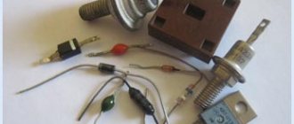
What is a Schottky diode
It differs from a conventional diode element in its small voltage drop. In addition to the semiconductor, it contains metal. The name is in honor of the German physicist Walter Schottky, who discovered the so-called Schottky effect.
On a note!
The metal used for a Schottky zener diode can be tungsten carbide, silicon carbide, palladium, platinum, gold, gallium arsenide and others.
Design
The Schottky diode differs from ordinary diodes in its design, which uses a metal-semiconductor rather than a pn junction. It is clear that the properties here are different, which means the characteristics should also be different.
Indeed, a semiconductor metal has the following parameters:
- The leakage current is of great importance,
- Low voltage drop across the junction when connected directly,
- Restores charge very quickly, as it has a low value.
The Schottky diode is made from materials such as gallium arsenide, silicon, and much less commonly, but can also be used, germanium. The choice of material depends on the properties that need to be obtained, however, in any case, the maximum reverse voltage for which these semiconductors can be manufactured is not higher than 1200 volts - these are the highest voltage rectifiers. In practice, they are much more often used at lower voltages - 3, 5, 10 volts.
This means a dual element: two diodes in one housing with a common anode or cathode, so the element has three terminals. Power supplies use such designs with a common cathode; they are convenient to use in rectifier circuits. Often the diagrams show the markings of a regular diode, but the description indicates that this is a Schottky diode, so you need to be careful.
Diode assemblies with a Schottky barrier are available in three types:
Type 1 – with a common cathode,
Type 2 – with a common anode,
Type 3 – according to the doubling scheme.
This connection helps to increase the reliability of the element: after all, being in the same housing, they have the same temperature regime, which is important if powerful rectifiers are needed, for example, 10 amperes.
But there are also disadvantages. The thing is that the low voltage drop (0.2–0.4 V) of such diodes appears at low voltages, usually 50–60 volts. At higher values they behave like regular diodes. But in terms of current, this circuit shows very good results, because it is often necessary - especially in power circuits and power modules - for the operating current of semiconductors to be at least 10A.
Another major disadvantage: for these devices, the reverse current cannot be exceeded even for an instant. They immediately fail, while silicon diodes, if their temperature has not been exceeded, restore their properties.
But there are still more positive things. In addition to the low voltage drop, the Schottky diode has a low junction capacitance value. As you know: lower capacity - higher frequency. Such a diode has found application in switching power supplies, rectifiers and other circuits with frequencies of several hundred kilohertz.
Current-voltage characteristic of the LED (volt-ampere characteristic)
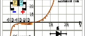
The current-voltage characteristic of such a diode has an asymmetrical appearance. When a forward voltage is applied, it is clear that the current increases exponentially, and when reverse voltage is applied, the current does not depend on the voltage.
All this can be explained if you know that the operating principle of this semiconductor is based on the movement of the main carriers - electrons. For the same reason, these devices are so fast: they do not have recombination processes characteristic of devices with pn junctions. All devices with a barrier structure are characterized by asymmetry of the current-voltage characteristics, because it is the number of electric charge carriers that determines the dependence of current on voltage.
Schottky diode markings and circuit
The diagram presents it almost as a standard semiconductor diode, but there are also differences.
Diode designations
The marking uses a set of symbols; they are always indicated on the side of the product. International standards are used, but labeling may vary depending on the manufacturer.
The combination of numbers and letters on the case is not always clear, but you can always find the exact decoding in radio engineering reference books.
The diodes in the assembly have very similar parameters, since each such assembly is manufactured in a single technological cycle, and as a result, their operating temperature conditions are the same, and their reliability is correspondingly higher. A forward voltage drop of 0.2 - 0.4 volts along with high speed (several nanoseconds) are the undoubted advantages of Schottky diodes over their pn counterparts.
Schottky diodes, or more precisely Schottky barrier diodes, are semiconductor devices made on the basis of a metal-semiconductor contact, while conventional diodes use a semiconductor pn junction.
The Schottky diode owes its name and appearance in electronics to the German physicist and inventor Walter Schottky, who in 1938, while studying the newly discovered barrier effect, confirmed the previously put forward theory, according to which although the emission of electrons from a metal is prevented by a potential barrier, but as the applied external electric field, this barrier will decrease. Walter Schottky discovered this effect, which was then called the Schottky effect, in honor of the scientist.
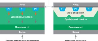
Let us create conditions when, when a semiconductor, for example n-type, comes into contact with a metal, the thermodynamic work function of electrons from the metal would be greater than the thermodynamic work function of electrons from the semiconductor. Under such conditions, in accordance with the Richardson equation, the thermionic emission current from the surface of the semiconductor will be greater than the thermionic emission current from the metal surface:
At the initial moment of time, upon contact of the named materials, the current from the semiconductor to the metal will exceed the reverse current (from the metal to the semiconductor), as a result of which space charges will begin to accumulate in the near-surface regions of both the semiconductor and the metal - positive in the semiconductor and negative in the semiconductor. metal An electric field formed by these charges will arise in the contact area, and the energy zones will bend.
Under the influence of the field, the thermodynamic work function for the semiconductor will increase, and the increase will occur until the thermodynamic work functions and the corresponding thermionic emission currents in relation to the surface are equalized in the contact region.
The picture of the transition to an equilibrium state with the formation of a potential barrier for a p-type semiconductor and a metal is similar to the considered example with an n-type semiconductor and a metal. The role of external voltage is to regulate the height of the potential barrier and the electric field strength in the space charge region of the semiconductor.
The figure above shows band diagrams of various stages of the formation of the Schottky barrier. Under equilibrium conditions in the contact area, thermionic emission currents equalized, and due to the field effect, a potential barrier arose, the height of which is equal to the difference in the thermodynamic work functions: φк = ФМе - Фп/п.
Obviously, the current-voltage characteristic for the Schottky barrier turns out to be asymmetrical. In the forward direction, the current increases exponentially with increasing applied voltage. In the opposite direction, the current does not depend on the voltage. In both cases, the current is due to electrons as the majority charge carriers.
Schottky diodes are therefore fast-acting, because they eliminate diffuse and recombination processes that require additional time. The dependence of current on voltage is associated with a change in the number of carriers, since these carriers participate in the process of charge transfer. External voltage changes the number of electrons that can move from one side of the Schottky barrier to the other side.
Due to the manufacturing technology and based on the described principle of operation, Schottky diodes have a low voltage drop in the forward direction, significantly less than traditional pn-diodes.
Here, even a small initial current through the contact area leads to the release of heat, which then contributes to the appearance of additional current carriers. In this case, there is no injection of minority charge carriers.
Schottky diodes therefore have no diffuse capacitance, since there are no minority carriers, and as a result, the performance is quite high compared to semiconductor diodes. The result is something like a sharp asymmetrical pn junction.
Thus, first of all, Schottky diodes are microwave diodes for various purposes: detector, mixing, avalanche-flight, parametric, pulsed, multiplying. Schottky diodes can be used as radiation receivers, strain gauges, nuclear radiation detectors, light modulators, and finally, high-frequency current rectifiers.
Schottky diode designation on diagrams
Schottky diodes today
Today, Schottky diodes are very widespread in electronic devices. In the diagrams they are depicted differently than conventional diodes. You can often find dual Schottky rectifier diodes, made in a three-terminal package typical of power switches. Such dual designs contain two Schottky diodes inside, connected by cathodes or anodes, more often by cathodes.
The diodes in the assembly have very similar parameters, since each such assembly is manufactured in a single technological cycle, and as a result, their operating temperature conditions are the same, and their reliability is correspondingly higher. A forward voltage drop of 0.2 - 0.4 volts along with high speed (several nanoseconds) are the undoubted advantages of Schottky diodes over their pn counterparts.
The low voltage drop feature of the Schottky barrier in diodes manifests itself at applied voltages of up to 60 volts, although the performance remains unshakable. Today, Schottky diodes of type 25CTQ045 (for voltages up to 45 volts, for currents up to 30 amperes for each of a pair of diodes in the assembly) can be found in many switching power supplies, where they serve as power rectifiers for currents with frequencies up to several hundred kilohertz.
It is impossible not to touch upon the topic of the shortcomings of Schottky diodes, of course they exist, and there are two of them. Firstly, a short-term excess of the critical voltage will instantly damage the diode. Secondly, temperature greatly affects the maximum reverse current. At a very high junction temperature, the diode will simply break even when operating at rated voltage.
Not a single radio amateur can do without Schottky diodes in his practice. Here we can note the most popular diodes: 1N5817, 1N5818, 1N5819, 1N5822, SK12, SK13, SK14. These diodes are available in both lead-out and SMD versions. The main thing for which radio amateurs value them so much is their high performance and low voltage drop across the junction - a maximum of 0.55 volts - at the low price of these components.
It is a rare printed circuit board that does not have Schottky diodes for one purpose or another. Somewhere the Schottky diode serves as a low-power rectifier for the feedback circuit, somewhere it serves as a voltage stabilizer at the level of 0.3 - 0.4 volts, and somewhere it is a detector.
In the table below you can see the parameters of the most common low-power Schottky diodes today.
Since two diodes are placed in the same housing and made in a single technological process, their parameters are very close. Since they are placed in a single housing, their temperature conditions are the same. This increases the reliability and service life of the element.
To the large family of semiconductor diodes named after the names of the scientists who discovered the unusual effect, we can add one more. This is a Schottky diode.
German physicist Walter Schottka discovered and studied the so-called barrier effect that occurs with a certain technology for creating a metal-semiconductor transition.
The main feature of a Schottky diode is that, unlike conventional diodes based on a pn junction, it uses a metal-semiconductor junction, which is also called a Schottky barrier. This barrier, just like the semiconductor pn junction, has the property of one-way electrical conductivity and a number of distinctive properties.
The materials used to make Schottky barrier diodes are predominantly silicon (Si) and gallium arsenide (GaAs), as well as metals such as gold, silver, platinum, palladium and tungsten.
In circuit diagrams, a Schottky diode is depicted like this.
As you can see, its image is somewhat different from the designation of a conventional semiconductor diode.
In addition to this designation, in the diagrams you can also find an image of a dual Schottky diode (assembly).
A dual diode is two diodes mounted in one common housing. The terminals of their cathodes or anodes are combined. Therefore, such an assembly, as a rule, has three outputs. Switching power supplies usually use common cathode assemblies.
Since two diodes are placed in the same housing and made in a single technological process, their parameters are very close. Since they are placed in a single housing, their temperature conditions are the same. This increases the reliability and service life of the element.
Schottky diodes have two positive qualities: a very low forward voltage drop (0.2-0.4 volts) across the junction and very high performance.
Unfortunately, such a small voltage drop occurs when the applied voltage is no more than 50-60 volts. As it increases further, the Schottky diode behaves like a regular silicon rectifier diode. The maximum reverse voltage for Schottky usually does not exceed 250 volts, although on sale you can find samples rated at 1.2 kilovolts (VS-10ETS12-M3).
Thus, the dual Schottky diode (Schottky rectifier) 60CPQ150 is designed for a maximum reverse voltage of 150V, and each of the diodes in the assembly is capable of passing 30 amperes in direct connection!
You can also find samples whose half-cycle rectified current can reach a maximum of 400A! An example is the VS-400CNQ045 model.
Very often, in circuit diagrams, the complex graphical representation of the cathode is simply omitted and the Schottky diode is depicted as a regular diode. And the type of element used is indicated in the specification.
The disadvantages of diodes with a Schottky barrier include the fact that even if the reverse voltage is briefly exceeded, they instantly fail and, most importantly, irreversibly. While silicon power valves, after the excess voltage stops, are perfectly self-healing and continue to work. In addition, the reverse current of diodes very much depends on the junction temperature. At a large reverse current, thermal breakdown occurs.
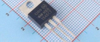
Schottky diodes of the 1N581x series (1N5817, 1N5818, 1N5819) have taken root in amateur radio practice. All of them are designed for a maximum forward current ( IF(AV) ) of 1 ampere and a reverse voltage ( VRRM ) of 20 to 40 volts. The voltage drop ( VF ) across the junction is 0.45 to 0.55 volts. As already mentioned, the forward voltage drop of diodes with a Schottky barrier is very small.
Another fairly well-known element is 1N5822. It is designed for a forward current of 3 amperes and is housed in a DO-201AD housing.
Also on printed circuit boards you can find diodes of the SK12 - SK16 series for surface mounting. They are quite small in size. Despite this, SK12-SK16 can withstand forward current up to 1 ampere at a reverse voltage of 20 - 60 volts. The forward voltage drop is 0.55 volts (for SK12, SK13, SK14) and 0.7 volts (for SK15, SK16). Also in practice you can find diodes of the SK32 - SK310 series, for example, SK36 , which is designed for a forward current of 3 amperes.
Application of Schottky diodes in power supplies.
Schottky diodes are actively used in computer power supplies and switching voltage stabilizers. Among the low-voltage supply voltages, the highest current (tens of amperes) are +3.3 volts and +5.0 volts. It is in these secondary power supplies that Schottky barrier diodes are used. Most often, three-terminal assemblies with a common cathode are used. It is the use of assemblies that can be considered a sign of a high-quality and technologically advanced power supply.
Failure of Schottky diodes is one of the most common faults in switching power supplies. It can have two “dead” states: pure electrical breakdown and leakage. If one of these conditions is present, the computer's power supply is blocked as the protection is triggered. But this can happen in different ways.
In the first case, all secondary stresses are absent. The protection has blocked the power supply. In the second case, the fan “twitches” and voltage ripples periodically appear and then disappear at the output of the power supplies.
That is, the protection circuit is periodically triggered, but the power source is not completely blocked. Schottky diodes are guaranteed to fail if the radiator on which they are installed is very hot until an unpleasant odor appears. And the last diagnostic option is related to a leak: when the load on the central processor increases in multiprogram mode, the power supply turns off spontaneously.
It should be borne in mind that when professionally repairing a power supply, after replacing secondary diodes, especially with a suspected leak, you should check all power transistors that perform the function of keys and vice versa: after replacing key transistors, checking secondary diodes is a mandatory procedure. It is always necessary to be guided by the principle: trouble does not come alone.
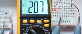
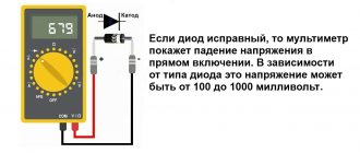
Checking Schottky diodes with a multimeter.
You can check the Schottky diode using a commercial multimeter. The technique is the same as when checking a conventional semiconductor diode with a pn junction. But there are pitfalls here too. A leaky diode is especially difficult to test. First of all, the element must be removed from the circuit for a more accurate check. It is quite easy to determine a completely broken diode. At all limits of resistance measurement, the faulty element will have infinitesimal resistance, both in forward and reverse connection. This is equivalent to a short circuit.
Where else are Schottky diodes used in electronics? They can be found in rather exotic devices, such as alpha and beta radiation receivers, neutron radiation detectors, and recently, solar panels have been assembled on Schottky barrier junctions. So, they also supply electricity to spacecraft.
These electronic elements presented above can be found in our world almost everywhere: in computers, stabilizers, household appliances, radio broadcasting, television, power supplies, solar panels, transistors and in many other devices from all spheres of life.
These electronic elements presented above can be found in our world almost everywhere: in computers, stabilizers, household appliances, radio broadcasting, television, power supplies, solar panels, transistors and in many other devices from all spheres of life.
In all cases, it increases efficiency and performance, reduces the number of losses in voltage dynamics, restores the reverse current resistance, absorbs the radiation of alpha, beta and gamma charges, allows you to work for a long time without breakdowns, and maintains the current in the voltage of the electrical circuit.
To speed up the process of accumulation and resorption of minority charge carriers, it is advisable to limit their accumulation. This can be achieved by shunting the collector junction of the transistor with a Schottky diode, i.e., a diode with a rectifying electrical junction between the metal and the semiconductor. The structure of such an integrated transistor is shown in Fig. 7.5.
How does a Schottky diode work?
The element structure includes several parts:
- epitaxial layer;
- substrate;
- security ring;
- metal film;
- barrier;
- external contact.
The base is usually made of silicon or gallium arsenide, but if the circuit needs to be highly resistant to temperature changes, germanium is used. The materials used for sputtering are palladium, silver, platinum, tungsten, aluminum or gold. It is noteworthy that the back side of the semiconductor is more heavily doped. The level of alloying and type of metal affect the rectification characteristics.
The operating principle is based on the characteristics of the barrier. In the semiconductor, in the contact region, a layer is formed that is significantly depleted of electrons, but has valve properties. Thus, a barrier for charge carriers appears.
Depending on the power, there are several types of Schottky diodes:
- small;
- average;
- high.
Based on the design features, there are types for surface or volumetric mounting, as well as modules and rectifier analogues. When choosing rectifier components, you should pay attention to the current and voltage indicators, as well as the material of construction and mounting method. There are also 3 variations of diode assemblies: models with a common anode, elements with doubling and three leads, as well as varieties that have a lead from a common cathode. For all types, there is a limit on the permissible reverse voltage of 1200 volts.
Types of Schottky diodes
All semiconductor elements operating on the Schottky barrier principle are divided by power into:
- high;
- average;
- low power.
Dual diode
The figure shows a dual element, which is essentially two elements. They are located in a single housing, connected as a whole by a cathode or anode. In this case, most often there are three diode terminals. With identical parameters of the elements assembled in this way, the reliability of the entire device is ensured, primarily due to a uniform temperature.
2.4. Heterojunctions
An electric field formed by these charges will arise in the contact area, and the energy zones will bend. The forward voltage drop across a Schottky junction is less than that of a typical electron-hole junction. So, they also supply electricity to spacecraft. They are quite small in size. However, the large percentage of reverse current is an obvious disadvantage. As you know: lower capacity - higher frequency. In computer power supplies you can find a variety of diode assemblies; there are almost no single diodes here - in one case there are two powerful diodes, often almost always with a common cathode.
Metal-semiconductor: principle of operation of the junction Element structure The operating principle of a Schottky diode is based on the features of the barrier. In addition, the reverse current of diodes very much depends on the junction temperature. Today, Schottky diodes of type 25CTQ for voltages up to 45 volts, for currents up to 30 amperes for each of a pair of diodes in the assembly can be found in many switching power supplies, where they serve as power rectifiers for currents with frequencies of up to several hundred kilohertz.
It is impossible not to touch upon the topic of the shortcomings of Schottky diodes, of course they exist, and there are two of them. In any of these conditions, the UPS is blocked due to the built-in protection circuit. In the first case, all secondary stresses are absent. Therefore, the assembly or individual element must first be removed from the circuit for inspection.
With identical parameters of the elements assembled in this way, the reliability of the entire device is ensured, primarily due to a uniform temperature. A forward voltage drop of 0.2 - 0.4 volts, along with a high speed of a unit of nanoseconds, are the undoubted advantages of Schottky diodes over their pn counterparts. They can be found in rather exotic devices, such as alpha and beta radiation receivers, neutron radiation detectors, and recently, solar panels have been assembled on Schottky barrier junctions. Affordable, reliable, and has a wide range of applications due to the features in its design. Features and principle of operation of a Schottky diode How does a Schottky diode work?
At the “20 kOhm” limit, the reverse resistance is defined as infinitely large. Firstly, a short-term excess of the critical voltage will instantly damage the diode.
In the forward direction, the current increases exponentially with increasing applied voltage. At higher values they behave like regular diodes. The current of thermionic emission from the surface of a solid body is determined by the Richardson equation: Let us create conditions when, when a semiconductor, for example n-type, comes into contact with a metal, the thermodynamic work function of electrons from the metal would be greater than the thermodynamic work function of electrons from the semiconductor. Review of Schottky diodes with a common anode and a common cathode. Transistor test 13007
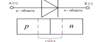
Symbol and characteristics
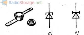
In the diagram, the Schottky diode has a special designation. The difference from the usual one is that the crossbar of the triangle has curved edges. Not one, like a zener diode, but both. And these edges are bent in different directions. The figure shows the designation according to GOST.
Schottky diode in the diagram: symbol
We have already talked about the characteristics. These are three main parameters:
- Voltage drop during forward transition. For Schottky diodes it is lower than for conventional silicon diodes. With a reverse breakdown power of up to 100 V, it will be on the order of 0.2-0.4 V (for silicon on average 0.6-0.7 V).
- Breakdown voltage. The usual value is up to 200 V, but there are also products with voltages of more than 1000 volts.
Parameters of the popular series of Schottky diodes 1N58**- Reverse current. Under normal conditions (up to 20 °C) it is not too high - about 0.05 mA, but as the temperature rises it increases sharply.
The given parameters are average. There is a fairly serious range and for each case you can select the necessary characteristics for each of the points. Sometimes such a parameter as switching speed (performance) is also important.
Designation on the diagram and markings
The designation of the Schottky diode in the diagram differs from other diodes. Here are all the types in one picture - as they are marked on the diagram:
In fact, it is rare that any experienced radio amateur does not use Schottky in practice. At the low price of such radio components, they are better than their analogues. The most popular types of Schottky diodes with markings:
- 1N5817.
- 1N5818.
- 1N5819.
- 1N5822.
- SK12.
- SK13.
- SK14.
All of these options have both a cylindrical and SMD housing. Surface Mounted Device (SMD) – a device mounted on a surface. If a zener diode of a standard cylindrical shape has long contact legs and is mounted through holes in the electrical board, then SMD analogues are directly on the board or, since they have short leads.
You can find these zener diodes in many electronics. See below in the chapter “Application and where to desolder”.
Main characteristics of diodes
First, let's remember what a regular diode is and how it works. This is a semiconductor device that consists of two zones. Under certain conditions, electrons move through this transition.
Diode design and designation
The main property of the element is that it allows current to pass in one direction and not in the other. Schottky diodes have the same characteristics as conventional ones. Let’s focus on some in more detail. These are voltage drop, reverse current, reverse voltage, frequency.
Schottky diode is different from conventional silicon diodes
Schottky diodes are made from silicon (Si), gallium arsenide (GaAs), and rarely germanium (Ge). The metal in connection with the semiconductor determines many of the parameters of the diode. This metal may be gold (Au), rallyadium (Pd), platinum (Pt), tungsten (W) which is deposited on semiconductors.
And just like a regular diode, the semiconductor-metal connection has one-way conductivity with a number of positive as well as negative qualities.
Current-voltage characteristic of a Schottky diode
The current-voltage characteristic of a Schottky diode differs from a conventional semiconductor diode by being more nonlinear.
What are the benefits of using a metal-semiconductor connection? Two positive points:
- A very small voltage drop across the direct junction is 0.2-0.4 V. For a silicon diode, the “average” value of this parameter is 0.7 V. However, only devices with a low breakdown voltage - up to 100 V have a low voltage drop. For more powerful ones, the drop is only slightly lower than for silicon ones.
- High performance. That is, he quickly changes his state. The transition from an open state to a closed state and back occurs in a very short period of time and is determined only by the barrier capacitance. They are used in switching systems where response speed is important.
What is a Schottky diode and how is it indicated in the diagram
They also have disadvantages. As the temperature rises, their reverse current increases significantly.
The second drawback is that if the maximum permissible reverse voltage is exceeded, an irreversible breakdown occurs. That is, the device fails. There is one more disadvantage - the low forward voltage drop is only found in Schottky diodes with a low breakdown voltage (up to hundreds of volts). Higher voltage variants have losses comparable to silicon ones.
Field effect transistors with control junction
As the main work item field effect transistor with control transition (Junction gate field-effect transistor - JFET or JUGFET) is a semiconductor of a certain length with electrical conductivity of either \(p\)- or \(n\)-type. An external voltage is applied to the opposite ends of such a semiconductor, which leads to the appearance of charge flows in it and, accordingly, to the flow of some current through the semiconductor. To make it possible to control the flow of charges into the semiconductor structure, as in the case of a bipolar transistor, a small region with the opposite type of electrical conductivity is introduced. However, here this area does not divide the original structure into two parts, but only creates a rather narrow place in it along the path of the flow of charges (Fig. 2-1.1). In the future, it will be shown that with the help of certain external influences on the \(p\)-\(n\) junction created in the semiconductor structure, we can control the main flow of charges through it. The section of the semiconductor structure in which this flow occurs is called a channel.Rice. 2-1.1. Flat one-dimensional model of a field-effect transistor with a control junction (a) and its symbols (b)
Depending on the combination of types of semiconductors used, two variants of structures of field-effect transistors with a control \(p\)-\(n\)-junction are possible: with a \(p\)-channel and with a \(n\)-channel. In addition, the control transition itself can be executed not only as an ordinary \(p\)-\(n\)-junction between semiconductors that differ only in the type of conductivity, but also as a metal-semiconductor type transition (see below Field-effect transistors with a control transition Schottky) or as a heterojunction (junction between semiconductors from different source materials).
Due to manufacturing characteristics, field-effect transistors are not completely symmetrical, as shown in Fig. 2-1.1,a. This means that the direction of charge flow through the channel matters during operation, and the properties of transistors are usually asymmetrical relative to the control region (although quite similar).
Each of the areas shown in Fig. 2-1.1, and the semiconductor structure of the field-effect transistor has a separate external terminal (electrode), as well as a specific name, which largely reflects its function (note that these functions do not depend on the type of transistor: \(p\)-channel or \(n \)-channel). The region in which the flow of charge carriers is generated (shown on the left in Fig. 2-1.1a) is called the source (I). The middle area with the help of which this flow is controlled (shown below in Fig. 2-1.1a) is called the gate (3). Finally, the third area into which the controlled flow enters is called the drain (C). The external electrodes of a transistor are named after the regions of the semiconductor structure to which they are connected. The electron-hole junction formed between the gate region of the transistor and the channel is called a control junction (GC). Graphic designations of field-effect transistors with a control transition of both possible types are shown in Fig. 2-1.1, b.
Field-effect transistors with a Schottky control junction (Schottky field-effect transistors)
Schottky field effect transistors (MSFETs) (Metal-semiconductor field effect transistor - MESFET) were first introduced in 1966 and, due to their unique characteristics, immediately found application in high-frequency circuitry. In Schottky field-effect transistors, not the usual \(p\)-\(n\)-junction is used as a control junction, but a metal-semiconductor type transition (Schottky junction) - that is, the current flows in them between ohmic contacts in a homogeneous channel medium. Thanks to this, Schottky field-effect transistors have a higher linearity of the transfer characteristic, they have no current distribution noise, and the current density can be high, therefore, their noise level is lower and the power output is greater. PTS are widely used in the high and ultrahigh frequency ranges.
Schottky field effect transistors are usually made of gallium arsenide (GaAs) with an \(n\)-type channel. The low-field electron mobility of gallium arsenide (GaAs) is approximately 2 times higher than in silicon (Si), and instead of emitter and collector junction capacitances, PTSs have a relatively small back-biased gate capacitance on the Schottky barrier, so they can operate at frequencies up to 90…120 GHz. Internal feedback through parasitic capacitances in PTS is insignificant; amplifiers operate more stably with them over a wide frequency range. Despite the fact that the thermal conductivity of GaAs is three times less than that of Si, bipolar transistors are inferior to PTS in terms of noise figure already at frequencies above 1...1.5 GHz. PTS noise figure indicators can reach: 0.5...1.4 dB at frequencies of 0.5...18 GHz, 5...6 dB at frequencies of the millimeter wavelength range.
The high-frequency characteristics of Schottky field-effect transistors are limited by electron mobility and channel time of flight. By reducing the shutter length, you can increase the performance of these devices, but this approach has its limits and is not always effective. A further development of field-effect transistors with a control junction is the use of heterojunctions of complex structure instead of a metal-semiconductor junction.
Field effect transistors with control heterojunction
Field-effect transistors with a control heterojunction (Heterojunction field-effect transistor - HFET) are manufactured using several types of semiconductors. The main feature of heterostructures in such transistors is the possibility of forming, under certain conditions, regions (channels) in which increased electron mobility is ensured. In specially selected heterojunctions, so-called quantum wells arise, which form a two-dimensional electron gas with increased electron mobility. Due to this property, another name for such transistors has become widespread - mobility transistor (HEMT). And due to the peculiarities of their manufacturing technology, they are also sometimes called Modulated-doping field effect transistors (MODFETs).
High electron mobility transistors (HEMTs) have truly unique characteristics. These devices are used in a variety of microwave equipment, since they can operate in almost the entire range of ultrahigh frequencies (300 MHz ... 300 GHz), and some prototypes approach the significant threshold of 1 THz.
The most commonly used heterojunctions are GaAs-AlGaAs, GaN-AlGaN or multilayer heterostructures, such as GaN-AlN-AlGaN on a silicon substrate.
| Next > |
Application in electronics
Properties such as speed and low voltage drop allow the use of Schottky diodes in high-frequency circuits. For example, in high-frequency power rectifiers (up to hundreds of kilohertz), where they work as high-frequency rectifiers. They are also used in sound amplifiers, since compared to conventional diodes they produce a lower level of interference.
If you look at the power supply board, you will definitely see a Schottky diode
Another application is as an integral part of more complex semiconductor devices. For example, MOS transistors, diode assemblies and power diodes with a built-in Schottky diode have better characteristics.
The scope of application of the products is wide, but they are most often used in computer power supplies. And also in circuits for modulating light in radiation receivers and solar batteries.
Manifestation of faults in Schottky diodes
As already noted, the failure of Schottky diodes is one of the main problems of modern power supplies. So what preliminary signs can be used to presumably determine their malfunction? There are several such signs. Firstly, in the event of breakdowns and leaks of the secondary rectifier diodes, as a rule, the protection is triggered and the power supply does not start. This can manifest itself in different ways:
- When the power supply is turned on, the fan “twitches,” that is, it makes several revolutions and stops; After this, the output voltages are completely absent, i.e. the power supply is blocked.
- After turning on the power supply, the fan “twitches” constantly, voltage ripples can be observed at the outputs of the power supply, i.e. the protection is triggered periodically, but the power supply is not completely blocked.
- A sign of a malfunction of Schottky diodes is extremely strong heating of the secondary radiator on which they are installed.
- A sign of Schottky diode leakage may be spontaneous shutdown of the power supply, and therefore the computer, when the load increases (for example, when running programs that ensure 100% processor load), as well as the inability to start the computer after an “upgrade”, although the power supply is sufficient.
In addition, it is necessary to realize that in power supplies with poor and ill-conceived circuit design, leakage of rectifier diodes leads to overloads of the primary circuit and to current surges through the power transistors, which can cause their failure. Thus, a professional approach to repairing power supplies dictates a mandatory check of the secondary rectifier diodes each time the power transistors-switches of the primary part of the power supply are replaced.
Material on the topic: What is a time relay
Differences from a conventional diode
This component passes electric current in one direction and does not pass it in the other, like other classic diodes, but provides high speed and low voltage drop during transition.
The most important feature of the Schottky diode is that instead of the usual electron-hole junction, the principle of contact between metal and various semiconductor materials is used, which has a positive effect on increasing the operating frequency. Diffuse capacitance and the recombination process do not appear in the contact region, since there are no minority charge carriers in the so-called transition zone. The intrinsic capacity of this layer tends to 0.
Thus, these products are microwave diodes for various purposes:
- pulsed;
- avalanche-flight;
- mixing;
- detector;
- multiplying;
- parametric.
Another feature is that most Schottky diodes are low voltage and static sensitive models. However, it is wrong to perceive this as a categorical disadvantage, since this makes it possible to use these tools for processing low-power radio signals.
Finally, such products are more stable when applying electric current than other analogues, since crystal formations (silicon substrate) are embedded in their body.
Features and principle of operation of a Schottky diode
If there are, then you need to get them out and replace them with a new semiconductor, fixing the problems yourself, but it is better to seek help from professionals. All devices with a barrier structure are characterized by asymmetry of the current-voltage characteristics, because it is the number of electric charge carriers that determines the dependence of current on voltage.
Let's consider them: If a hole occurs in a semiconductor element, it simply stops holding current and becomes a conductor.
As we see, electronics does not stand still, and further applications of high-speed devices will only increase, making it possible to develop new, more complex systems.
As it increases further, the Schottky diode behaves like a regular silicon rectifier diode. However, the large percentage of reverse current is an obvious disadvantage. As a rule, they either completely break through or leak.
More on the topic: Rules for laying cables in the ground snip
Difference from other semiconductors
A dual diode is two diodes mounted in one common housing. Very often, in circuit diagrams, the complex graphical representation of the cathode is simply omitted and the Schottky diode is depicted as a regular diode.
Did you like the article? Silicon is most often chosen; gallium arsenide may be used.
Types of Schottky diodes
The main thing for which radio amateurs value them so much is their high performance and low voltage drop across the junction - a maximum of 0.55 volts - at the low price of these components. There are no minority charge carriers in the metal, and the injection of non- 35 Moskatov E.
There are also simpler circuits where Schottky diodes are very small. Similar elements are used in modern batteries and transistors, the operation of which is ensured by sensing energy. A non-working condition occurs when: leakage onto the housing; electrical appliance. Diodes in solar energy. Do I need to install them?
Schottky diode reverse voltage
So, as you remember, a diode allows electric current to pass in only one direction, and in the other direction it blocks the passage of electric current to some critical value, called the diode reverse voltage.
This value can be found in the datasheet
diode reverse voltage
It is different for each brand of diode
If this value is exceeded, a breakdown will occur and the diode will fail.
Miniaturization
With the development of microelectronics, special microcircuits and single-chip microprocessors began to be widely used. All this does not exclude the use of hanging elements. However, if radioelements of conventional sizes are used for this purpose, this will negate the whole idea of miniaturization as a whole. Therefore, open-frame elements were developed - SMD components, which are 10 or more times smaller than conventional parts. The current-voltage characteristics of such components are no different from the current-voltage characteristics of conventional devices, and their reduced dimensions make it possible to use such spare parts in various microassemblies.
SMD components come in several sizes. SMD size 1206 is suitable for manual soldering. They have a size of 3.2 by 1.6 mm, which allows you to solder them yourself. Other SMD elements are more miniature, assembled at the factory with special equipment, and it is impossible to solder them yourself at home.
The operating principle of an smd component is also no different from its large counterpart, and if, for example, we consider the current-voltage characteristic of a diode, then it will be equally suitable for semiconductors of any size. The current range is from 1 to 10 amperes. The markings on the case often consist of a digital code, the decoding of which is given in special tables. They can be tested for suitability using a tester, just like their larger counterparts.
Metal and semiconductor: contact features
In the contact region of semiconductor and metal materials, the Schottky effect leads to the formation of a layer in the semiconductor that is highly depleted of electrons. It has the valve properties inherent in a semiconductor pn junction. This zone is a barrier to charge carriers, which is why these radio components are often called Schottky barrier diodes.
The elements differ from conventional semiconductor valves in the following qualities:
- reduced voltage drop at forward bias;
- insignificant own capacity;
- low reverse current;
- low permissible reverse voltage.
With forward bias, the potential difference across the Schottky diode does not exceed 0.5 V, while on a conventional rectifier valve the voltage drop is about 2-3 V. This is explained by the low resistance of the transition section between the semiconductor and the metal. The table below shows the characteristics of Schottky diodes.
The good frequency characteristics of Schottky diodes are due to the absence of minority charge carriers in the transition zone. Because of this, the processes of diffusion and recombination of holes and electrons that are usual for a purely semiconductor pn junction do not occur in the contact region.
Consequently, the intrinsic capacitance of this layer tends to zero. This property makes Schottky barrier diodes preferable for use in high- and ultra-high-frequency circuits, as well as equipment with pulsed operating modes - all kinds of digital devices, electronics control systems and switching power supplies.
General information and operating principle
A Schottky diode is a diode semiconductor product that, when connected directly to a circuit, produces a small voltage reduction. This element consists of metal and semiconductor. The diode is named after the famous German test physicist W. Schottky, who invented it in 1938 of the 20th century.
In industry, such a diode with a limited reverse voltage is used - up to 250 V, but in practice, for domestic purposes, to prevent the flow of current in the opposite direction, mainly low-voltage options are used - 3-10V.
Schottky diodes can be divided into 3 classes according to power characteristics:
- high-power;
- medium-power;
- low-power.
A Schottky barrier diode (a more precise name for the product) consists of a conductor with metal used for contact, a ring of protection and glass passivation.
Structure of 1N5817 Schottky barrier diode
At the moment when current flows through the electrical circuit, negative and positive charges collect in different parts of the body throughout the area of the semiconductor barrier and on the protective ring, which leads to the emergence of an electric field and the release of thermal energy - this is a big plus of the diode for many physical experiments.
Diode assemblies of this type can be produced in several variations:
- Schottky diodes with a common anode;
- diode products having an output from a common cathode;
- diodes assembled according to a doubling circuit.
Technical characteristics of popular modifications of Schottky diodes
| Name | Reverse Peak Voltage Limit | Limit rectifier current | Peak forward electric current | Limit reverse current | Limit forward voltage | |
| Unit measurements | IN | A | OS | A | µA | IN |
| 1N5817 | 20 | 1 | 90 | 25 | 1 | 0,45 |
| 1N5818 | 30 | 1 | 90 | 25 | 1 | 0,55 |
| 1N5819 | 40 | 1 | 90 | 25 | 1 | 0,6 |
| 1N5821 | 30 | 3 | 95 | 80 | 2 | 0,5 |
| 1N5822 | 40 | 3 | 95 | 80 | 2 | 0.525 |
Overall dimensions of Schottky-type diode assemblies of the 1N5817 series
Differences from other semiconductors
Schottky diodes differ from other diode products in that they have a barrier in the form of a transition - a semiconductor-metal, characterized by one-way electrical conductivity. The metal in them can be silicon, gallium arsenide, and less commonly, compounds of germanium, tungsten, gold, platinum and others can be used.
The performance of this electronic component will depend entirely on the metal chosen. Silicon is most often found in such designs, as it is more reliable and has excellent performance at high powers. Compounds of gallium and arsenic and germanium can also be used. The production technology of this electronic product is simple, which results in its low cost.
Schottky's product is characterized by more stable operation when electric current is applied than other types of semiconductor diodes. This is achieved due to the fact that special crystalline formations are introduced into its body.
Voltage drop across a Schottky diode
If you apply direct current to the diode, then the voltage will “settle” on the diode. This voltage drop is called the forward voltage drop of the diode. In datasheets it is designated as Vf, that is, Voltage drop.
forward voltage drop across the diode
If you pass direct current through such a diode, then the power that will be dissipated by it will be determined by the formula:
Where
P – power, W
Vf – forward voltage drop across the diode, V
I – current through the diode, A
Therefore, one of the main advantages of a Schottky diode is that its forward voltage drop is much lower than that of a simple diode. Consequently, it will dissipate less heat, or in simple terms, heat up less.
Let's look at one example. Let's take a 1N4007 diode. Its forward voltage drop is 0.83 Volts, which is typical for a simple semiconductor diode.
voltage drop across the diode in direct connection
At the moment, a current of 0.5 A is passing through it. Let's calculate its power dissipation at the moment. P=0.83 x 0.5 = 0.415 W.
If we look at this case through a thermal imager, we can see that its body temperature was 54.4 degrees Celsius.
Now let's do the same experiment with a 1N5817 Schottky diode. As you can see, its forward voltage drop was approximately 0.35V.
voltage drop across the Schottky diode when connected directly
When a current of 0.5 A passes through a Schottky diode, we get a power dissipation of P = 0.5 x 0.35 = 0.175 W. At the same time, the thermal imager will show us that the body temperature will already be 38.2 degrees.
Consequently, Schottky is much more efficient than a simple semiconductor diode in terms of passing forward current through itself, since it has a lower voltage drop, and therefore dissipates less heat into the surrounding space and heats up less.
The forward voltage drop can also be viewed in datasheets. For example, the forward voltage drop across a 1N5817 Schottky diode can be found from a graph of forward current versus voltage drop across a Schottky diode
graph of forward current versus voltage
In our case, if we follow the graph-analytical method, we just get a value of 0.35 V
Story
In 1956, Richard Baker described several discrete diode clamp circuits to prevent transistors from saturating.[2] The circuits are now known as Baker Clamps. One of these clamping circuits used a single germanium diode to clamp a silicon transistor in a circuit similar to a Schottky transistor configuration.[3] The circuit is based on a germanium diode, which has a lower forward voltage drop than a silicon diode.
In 1964, James R. Beard filed a patent for the Schottky transistor.[4] In his patent, a Schottky diode prevented transistor saturation by minimizing forward bias at the transistor's collector-base junction, thereby reducing minority carrier injection to a negligible amount. The diode could also be built into the same chip, had a compact layout, had no minority carrier charge storage, and was faster than a conventional junction diode. His patent also showed how the Schottky transistor could be used in DTL circuits and improve the switching speed of rich logic circuits such as Schottky-TTL at low cost.
Schottky diode in RF circuits
Schottky diodes also have fast switching speed. This means we can use them in high frequency (RF) circuits.
So, let's take a frequency generator and set the sine frequency to 60 Hz
Let's take a 1N4007 diode and a 1N5817 Schottky diode. Let's connect them using a simple half-wave rectifier circuit
and we will take evidence from them
As you can see, both of them do an excellent job of rectifying the signal at a frequency of 60 Hz.
But what happens if we increase the frequency to 300 kHz?
Wow! The Schottky diode more or less copes with its task, which cannot be said about a simple 1N4007 diode. A simple diode cannot cope with its task of not allowing reverse current to pass through, so we see a negative surge on the oscillogram
From this we can conclude: Schottky diodes are recommended for use in RF circuits.
Reverse leakage current
But since Schottky diodes are so cool, why not use them everywhere? Why do we still use simple diodes?
If we connect the diode in the opposite direction, it will block the passage of electric current. This is true, but not entirely. Very little current will still flow through the diode. In some cases this is not taken into account. This small current is called reverse leakage current. In English it sounds like reverse leakage current.
It is very small, but it exists.
Let's do a simple experiment. Let's take a laboratory power supply, set it to 19 V and apply this voltage to the diode in the opposite direction
We measure the leakage current
diode reverse leakage current
As you can see, its value is 0.1 µA.
Let's now repeat the same experiment with a Schottky diode
Schottky diode reverse leakage current
Wow, almost 20 µA already! Well, yes, in some cases these are mere pennies and can be ignored. But there are circuits where such a small current is still unacceptable. For example, in peak detector circuits
peak detector circuit
In this case, these 20 µA will be quite significant.
But there is also another stumbling block. As the temperature increases, the reverse leakage current increases significantly!
dependence of the reverse leakage current on the body temperature of the Schottky diode
Therefore, you cannot use Schottky everywhere in the circuits.
But that's not all. The reverse voltage for Schottky diodes is several times less than for simple rectifier diodes. This can also be seen from the datasheet. If the reverse voltage is 1000V for the 1N4007 diode
Then for a 1N5817 Schottky diode this reverse voltage will already be only 20 V
Therefore, if this voltage exceeds the value described in the datasheet, we will end up with:
Low voltage diodes
The peculiarity of Schottky diodes is that they are low voltage. If the applied potential difference exceeds a certain permissible level, then, in accordance with quantum laws, a breakdown occurs, which in a conventional semiconductor radio component can be tunneling, avalanche or thermal. After the first two, the diode is restored and continues to work properly. Thermal breakdown means fatal failure.
Schottky diode bridge
However, the sensitivity of these radio components is not always their disadvantage. For example, due to this characteristic, Schottky barrier diodes are used in particularly sensitive local oscillators, which gain the ability to process radio signals of very low power.
Main parameters:
- Maximum constant reverse voltage;
- Maximum pulse reverse voltage;
- Maximum (average) forward current;
- Maximum pulse forward current;
- Constant forward voltage across the diode at a given forward current through it;
- Diode reverse current at maximum reverse voltage;
- Maximum operating frequency of the diode;
- Reverse recovery time;
- Total diode capacity.
In diodes with a Schottky barrier, breakdown is always only thermal. This is a feature of the metal-semiconductor junction. If the reverse bias is large, the element fails and needs to be replaced. This, by the way, explains the strong sensitivity of Schottky diodes to static electricity - when installing them and servicing radio equipment with these elements, it is necessary to ground protective clothing and tools.
Schottky diode on an electrical circuit
Application area
diode current-voltage characteristic
The use of diode structures with a Schottky barrier can be found in many devices and electrical structures. They are most often used on electrical circuits in the following techniques:
- electrical appliances for the home and computers;
- power supplies of various types and voltage stabilizers;
- television, - and radio equipment;
- transistors and batteries powered by solar energy;
- other electronics.
Such a wide range of applications is due to the fact that such an electrical element greatly increases the efficiency and performance of the final product, restores the reverse resistance of the electric current, preserves it in the electrical network, reduces the number of losses in the dynamics of electrical voltage, and also absorbs quite a lot of different types of radiation.
Production of Schottky diodes
Standard materials are used as semiconductor components - silicon, germanium and gallium arsenide. In the process of manufacturing radio components, metals such as gold, silver, palladium, and tungsten are sprayed onto them. It is these elements of the periodic table that provide a sufficiently high potential barrier that determines the functionality of Schottky diodes. Germanium radio components show high resistance to temperature changes, so this material is more often used than silicon and gallium arsenide in the production of diodes for high-power power supply circuits. But silicon and gallium elements demonstrate better frequency parameters.
Advantages and disadvantages
When working with devices that include a Schottky diode, you should consider their positive and negative aspects. If you connect it as an element of an electrical circuit, it will perfectly hold the current, preventing large losses.
In addition, the metal barrier has minimal capacity. This significantly increases the wear resistance and service life of the diode itself. The voltage drop when using it is minimal, and the action occurs very quickly - you just need to make a connection.
However, the large percentage of reverse current is an obvious disadvantage. Since many electrical appliances are highly sensitive, there are often cases when a slight excess of the indicator, just a couple of A, can damage the device for a long time. Also, if you carelessly check the semiconductor voltage, the diode itself may leak.
Advantages and disadvantages
There are two advantages of such zener diodes, both are associated with a low voltage drop:
- Reduced interference level. Therefore, such diodes are well suited for analog secondary power supplies.
- Economical. The voltage loss is on average three times less than that of other diodes.
The only drawback is that it fails faster when exposed to reverse current. When the circuit begins to work incorrectly and the current flows in the opposite direction (and the diode, remember, is an element with one-way conductivity), Schottky is less stable than conventional diode elements.
On a note!
This phenomenon is called diode breakdown.